Design and Implementation of Pulse Width
Modulation Controller on FPGA using HDL
Sneha R. Kirnapure¹, Vijay R. Wadhankar²
P.G.Student, M.Tech (4thSem), Dept. of E &C, Agnihotri College of Engineering, Nagthana Road, Wardha (M.S),India¹
Professor, Dept. of E&C, Agnihotri College of Engineering, Nagthana Road, Wardha (M.S), India2
ABSTRACT:The project is concerned with the design, synthesis, and the implementation of pulse width modulation (PWM) on FPGA. The project develops high frequency PWM generator architecture by using FPGA. The resulting FPGA frequency depends on the target FPGA speed grade and the duty cycle resolution requirements.In the PWM architecture, we are going to design blocks like N-bitregister, N-bit counter, comparator and R S latch and complete PWM architecture is also design and simulated. The VHDL language is used in the design process of PWM.Quartus II version 13.0 software is used to perform the simulations. Pulse-width modulation (PWM) is a modulation technique that changes the width of the pulse, formally the pulse durationThe simulation was performed on the architecture and after verifying the results this VHDL code is implemented on Cyclone-IVE FPGA of family EP4CE115F29C7 by using Quartus-II software.
KEYWORDS:Pulse width modulation, Field programmable gate array, Hardware description language, Altera Quartus II
I. INTRODUCTION
Using pulse width modulation (PWM) in power electronics control system is not new, there are different approaches for developing pulse width modulation. Many digital circuits can generate PWM signals, but what is interesting is, to generate pulse width modulation using Hardware Description Language (VHDL) and implementing it on FPGA. FPGA implementation of PWM is selected because FPGA can process information faster, controller architecture, hardware design flexibility, design reuse.Pulse-width modulation (PWM) is a modulation technique that controls the width of the pulse, formally the pulse duration. The term duty cycle describes the proportion of 'on' time to the regular interval or 'period' of time; a low duty cycle corresponds to low power, because the power is off for most of the time. Duty cycle is expressed in percent, 100% being fully on.
FPGAs are configurable ICs (user can design, program and make changes to his circuit whenever he wants)and used to implement logic functions. Today’s FPGAs can hold several millions gates and have some significant advantage. They ensure ease of design, lower development costs and the opportunity to speed products to market.FPGA areprogrammable semiconductor devices that are based around a matrix of configurable logic block (CLBs) connected via programmable interconnects. FPGA can be programmed to the desired application or functionality requirement. VHDL is a language that is used to describe the behaviour of digital circuit designs. It is VHSIC (Very High Speed Integrated Circuit) Hardware Description Language , and now used extensively by industry and academia for the purpose of simulating and synthesizing digital circuit design. Its designs can be simulated and translated into a form suitable for hardware implementation.VHDL modelling is used to generate the PWM.
To design the PWM in Field programmable gate array, first the functional description of the design modelled in very high speed integrated circuit HDL and this VHDL code is synthesized and simulated using Quartus II software. After successfully synthesized and simulated the design it can be downloaded to the targeting device (FPGA).
Paper is organized as follows. Section II describes a literature survey related to this project as per referred to previous studies and results obtained by past researchers.Section III provides a methodology in how this project is conducted in sequence. Methodology describes block description of PWM controller. Section IV presents experimental results showing results. Finally, Section V presents conclusion
II. RELATEDWORK
The digital implementation of PWM is an important research area. The arrival of FPGA brings out a dramatic change in the digital PWM control applications. With FPGA, the researchers got a better alternative solution for the digital implementation of PWM .The content of this paper are based on various scholastic papers. Some of the papers are mention below and a brief idea of what they are about is mentioned. The digital implementation of PWM is an important research area.
In paper [7], results show that PWM frequencies up to 3.985 MHz can be produced using the proposed design method with a duty cycle resolution of 1.56% using the Xilinx Foundation software v3.1.
In paper [8], experimental results show that PWM frequency with an 8-bit data input was 46.875 kHzusing the XS40 v1.2 board, which contains the Xilinx 4010XLPC84-3 FPGA and PWM frequencies up to 3.985MHz can be produced with a duty cycle resolution of 1.56%.
In paper [9], generation of PWM signals with varying duty cycle using VHDL code and tested on FPGA. A FPGA SPARTAN3 board is used as hardware and ISE10.1 XILINX is used as software. The generated PWM signals have a fixed frequency 10MHz.
In paper [10], the generation of PWM signals is discussed using VHDL based on FPGA. A board SPARTAN3AN is used as a hardware and ISE14.4 XILINX is used as software. The generated PWM signals have a fixed frequency (11.8 KHz) depended on the frequency of sawtooth, and a variable duty cycle that changes from 0% to 100%.
In paper [11],there are two classes of PWM techniques identified optimal PWM and carrier PWM. The optimal PWM requires lot of computation and hence extra hardware and hence extra cost .Carrier PWM techniques require a carrier signal which is modulated with modulating signal to produce desired PWM signal. There are various methods depending upon architecture and requirement of the system. Their design implementation depends upon application type, power consumption, semiconductor devices, performance and cost criteria.
III.FUNTIONALDESCRIPTIONOFTHEPWMDESIGN
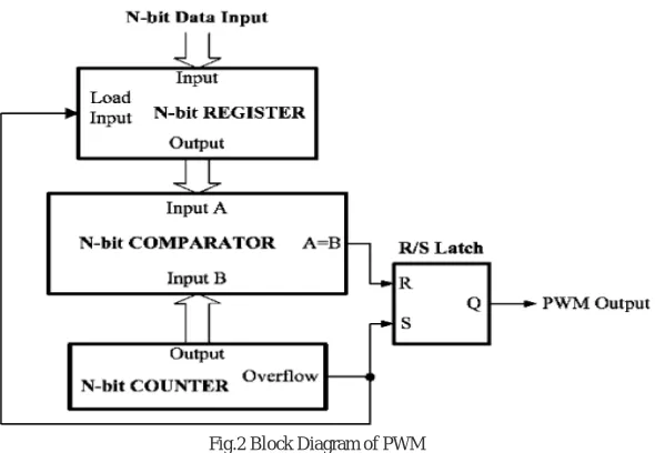
Fig.2 Block Diagram of PWM
The block diagram of the PWM architecture is shown in Fig.2. The system input is an N-bit dataword, corresponding to the desired PWM duty cycle value. The register stores the input to be processed .So when load input signal is ‘1’ the register provides input to output. The counter used is 8 bit up-counter. The N-bit register output, containing the N-bit data input, is compared with the output value of an N-bit counter, by means of a comparator. When these two values become equal, the comparator output is used to reset the R/S latch output which produces the PWM wave. The R/S latch output is set when the counter reaches an overflow condition at the end of a PWM period. Also, the counter overflow signal is used to load the N-bit data input to the input register. R S latch is used to set or reset the output. When ‘r’ signal is ‘1’ output is reset to ‘0’.When ‘s’ signal is ‘1’ output is set to ‘1’.
The duty cycle is given from the following equation: Duty Cycle = Data Value/2n
where, Data Value is the N-bit input data value.
For an 8 bit input, resulting in 28 different duty cycle states. The duty cycle of the PWM signal is controlled by the data value. The higher the data value the higher the duty cycle. If an 8-bit input is used, then the duty cycle is in the rangeof 0≤ D ≤ = 99.6%. Since the PWMduty cycle has 28
different states, the generator resolution,α, is defined as,
α =
ᶰ• 100% = ⁸•100%= 0.39%
Table 1: Some of the Data Values for different Duty Cycles (N=8)
Data value
Duty Cycles (%)
00011111 12.89
01111111 50.39
11100000 88.28
IV.DESIGNANDIMPLEMENTATION
A. Design of PWM Controller:
A software program using the VHDL language was developed, for synthesizing the PWM controller presented in the fig.2, using the Quartus II software. The RTL view and waveform of each block and complete block diagram is shown in figure below.From the simulated waveform we observe that higher the data value, higher the duty cycle and lower the data value, lower the duty cycle. The simulated results and waveforms of Fig.2 blocks are shown below:
N-bit Register
:
The N-bit register present in PWM generator has N-bit data input& 1 output. Register is used to store the input to be processed. So when load signal is ‘1’, the register provides input to output RTL view and waveform is shown in Fig.3 & 4.Fig.3 RTL view of Register
Fig.4 Simulated waveform of Register
N-bit Counter: Counter used is 8-bit up counter.The counter increases one bit and it counts from (00000000)2 to (11111111)2. The maximum value is (255)10, when PWM counter arrives to this value, it returns to zero.
Fig.6 Simulated waveform of Counter
N-bit Comparator:bit register output containing bit data input ,is compared with output value of an N-bit counter by means of a comparator.
Fig7 RTL view of Comparator
Fig.8 Simulated waveform of Comparator
R/S Latch: R S latch is used to set or reset the output. When ‘R’ signal is 1 output is reset to 0. When ‘S’ signal is 1 output is set to 1.
Fig.10 Simulated Waveform of R S latch
PWM Block:All the above 4 blocks are combined to form a complete PWM block whose connection are shown below in fig.11 and waveforms are shown in fig.12 and 13.
Fig.11 RTL view of PWM block
Fig.14 Design Flow Summary
B. Implementation of PWM Controller on FPGA:
First connect supply to DE2-115 board & connect USB cable to laptop & to USB blaster of the board, compile code, assign pins, choose JTAG programming mode & download the program into target device. After design, compile & simulation done of complete PWM block, it is downloaded into FPGA device EP4CE115F29C7.We can give input word ‘din’ as different 8-bit input combination to see how the output of FPGA varies. This input can be given by 8 switches present on FPGA boardand the output can be seen by one LED whose pin number has been assigned to PWM output.The clock for the architecture was provided by clock present on FPGA board. As we change the “din” value on the FPGA board by different configuration of switches. The snapshot of FPGA board with different 8-bit input value is shown with different LED intensity, if the input value is large then the intensity of LED is more and if the input value is small then the intensity of LED is less.
Fig.16Snapshot of FPGA device with input 11100000 & 11111000
V. CONCLUSION
In this paper, a high frequency PWM generator architecture, using FPGA has been presented,an 8 bit PWM was developed using VHDL. The simulation results show that, PWM frequency up to 250MHz can be produced with a duty cycle resolution of 0.39%.The selection of the target device depends on the system cost and resolution requirements.
REFERENCES
[1] SnehaKirnapure, Vijay R. Wadhankar ,’Review on Design of PWM Controller Using FPGA’ International Journal of ScienceandResearch(IJSR), Volume 4 Issue 4, April 2015 ,pp1489-1492,2015 .
[2] SnehaKirnapure, Vijay R. Wadhankar,’Design of Pulse Width Modulation Controller on FPGA using HDL’,International Journal of Innovative Research in Computerand Communication Engineering(An ISO 3297: 2007 Certified Organization)Vol. 3, Issue 7,pp 6785- 6790, July 2015.
[3] Brown,Vranesic,‘Fundamentals of Digital Logic with VHDL Design’, Tata McGraw Hill. [4] Wolf Wayne,”FPGA-Based System Design”,Pearson Education, Inc., USA, 2004. [5] FPGAs for DUMMIES ,Altera special Edition ,by Andrew Moore.
[6] Gwaltney, “FPGA Implementation of controls,” 2003.
[7] Jakirhusen I. Tamboli, Prof. Satyawan R. Jagtap, Amol R. Sutar ,’ Pulse Width Modulation Implementation using FPGA and CPLD IC’s’, International Journal of Scientific & Engineering Research Volume 3, Issue 8,pp 1-5, August-2012.
[8] EftichiosKoutroulis ,ApostolosDollas, Kostas Kalaitzakis,’High-frequency pulse width modulation implementation using FPGA &CPLD ICs’,Journal of Systems Architecture 52 (2006) 332–344,pp 332-344,Available online 25 October 2005
[9] Suneeta, R Srinivasan,Ramsagar,’Generation of Variable Duty Cycle PWM using FPGA’ ,IOSR Journal of VLSI and Signal Processing (IOSR-JVSP) Volume 4, Issue 6, Ver. II, PP 01-03 e-ISSN: 2319 – 4200, p-ISSN No. : 2319 – 4197 www.iosrjournals.org,pp-1-3, Nov - Dec. 2014.
[10] ZiadNouman, BohumilKlima, Jan Knobloch ‘Generating PWM Signals With Variable Duty From 0% to 100% Based FPGA SPARTAN3ANAl’Electrorevue ISSN 1213-1539 VOL.4, NO.4,pp 75-80, DECEMBER 2013.
[11] Rahim, N.A. and Islam Z.,’A single-phase series active power filter design’, Proceeding of the International Conference on Electrical, Electronic and Computer Engineering, IEEE XplorePress ,Sept. 2004, pp: 926-929.
[12] Dancy A.P., Amirtharajah R. and Chandrakasan A.P., ‘High-Efficiency Multiple-Output DC–DC Conversion for Low-Voltage Systems’, IEEE Trans. on Very Large Scale Integration (VLSI) Systems, Vol. 8, No. 3, June 2000: pp.252-263.
BIOGRAPHY
Sneha R.Kirnapurereceived her B.E. in Electronics from R.C.E.R.T.,Chandrapur, India in 2009.Currently she is pursuing M.Tech in Electronics from A.C.E.,Wardha, India.