ABSTRACT
BARLETTA, PHILIP. Study of GaN-based Materials for Light-emitting Applications. (Under the direction of Dr. S.M. Bedair and Dr. N.A. El-Masry).
The purpose of this study was to explore the possibility of fabricating phosphor-free white-emitting LED’s based in the gallium nitride material system. The structures were to be grown using metal-organic chemical vapor deposition (MOCVD). Toward this end, a Thomas Swan Scientific close-coupled showerhead reactor was installed.
The first experimental step in this project was the optimization of nominally undoped GaN. This was achieved successfully, as smooth, non-compensated, optically-active films were demonstrated. Additionally, a full on- and off-axis x-ray diffraction study showed that the crystal quality of this material compared favorably to that of published standards.
Successful n- and p-type doping of GaN were also demonstrated. Device-worthy mobility and carrier concentration values were demonstrated. Atomic force microscopy of n-type material verified that the films was sufficiently smooth as to serve as a layer upon which active-layer quantum wells could be grown. Photoluminescence of both n- and p-type material was examined as well.
This InGaN experimental work was complemented with a series of calculations which gave the expected emission wavelength of an InGaN/GaN quantum well structure based on In content and well width. Strain, the quantum size effect, and the quantum-confined Stark effect were all factored into these calculations in order to study their individual contributions to emission wavelength values.
This work concluded with an examination of white device structure and fabrication. Both two- and three-color devices were considered. Monochromtic devices emitting in the green and yellow were fabricated. The yellow device, emitting at 575nm, yielded the longest reported wavelengths for Al-free InGaN/GaN multiple quantum-well LED’s grown by MOCVD. Finally, white emission was demonstrated from a two-color MQW structure emitting blue and yellow light.
STUDY OF GaN-BASED MATERIALS FOR LIGHT-EMITTING APPLICATIONS
by
PHILIP BARLETTA
A dissertation submitted to the Graduate Faculty of North Carolina State University
in partial fulfillment of the requirements for the Degree of
Doctor of Philosophy
MATERIALS SCIENCE AND ENGINEERING
Raleigh 2006
APPROVED BY:
____________________________ ____________________________
Jerome J. Cuomo Carl C. Koch
____________________________ ____________________________
BIOGRAPHY
Philip Barletta was born on August 5, 1974 in Scranton, PA. In 1992 he began
studying materials science at Wilkes University in Wilkes-Barre, PA. In May of 1996 he
graduated Magna cum Laude from Wilkes, receiving a Bachelor of Science degree in
materials engineering.
Later that year Philip moved to Raleigh, NC, and began his studies at North
Carolina State University. He performed research at the Center for Advanced
Manufacturing Processes and Materials (CAMP-M) under the direction of Dr. Jerome J.
Cuomo. In December of 1999 he received his Master of Science degree in materials
science and engineering at N.C. State.
After a brief stint as a process engineer at Litespec Optical Fiber, Philip returned
to North Carolina State in the fall of 2000 to pursue his Ph.D. He was awarded a research
assistantship to work under Dr. Salah Bedair studying the MOCVD growth of compound
semiconductors.
On June 9, 2001, Philip married his long-time sweetheart, Kristin Thoney, at Holy
Trinity Lutheran Church in Raleigh, NC. Five years and one day later, Kristin gave birth
to their first child, John Philip “Jack” Barletta.
In November 2005, while still completing his studies, Philip accepted a job at Dot
Metrics Technologies, a start-up company in Charlotte, NC. In the summer of 2006, he
earned his Ph.D. degree in materials science and engineering at N.C. State. On July 31 of
that year, he began working for the Center for Thermoelectrics Research at RTI
ACKNOWLEDGEMENTS
Any time one undertakes a work of this magnitude, he (or she) cannot do it alone.
I’m no exception. I am indebted to a great number of individuals who have helped me
along the way, and I will now do my best to express my gratitude
I would like to start by thanking my advisor, Dr. Salah Bedair. Dr. Bedair’s
extensive knowledge, as well as his love of science, make him a truly exceptional mentor.
My experiences with him will certainly guide me as I continue along in my career. I
share the same sentiments for my co-advisor, Dr. Nadia El-Masry. She has played a huge
role in my graduate studies as well, and I owe her a tremendous debt of gratitude.
I would also like to thank the rest of my committee: Dr. Jerry Cuomo and Dr. Carl
Koch. I am especially indebted to Dr. Cuomo, as he was my M.S. advisor and helped
shape me into the scientist I am today. Dr. Koch has looked at my work from the point of
view of a metallurgist, and thus has provided some unique insights.
Thanks are also due to Dr. Steven LeBoeuf and Dr. Michael Aumer, two old
friends of mine who introduced me to Dr. Bedair and helped bring me into his laboratory.
They were also instrumental in teaching me the basics of both MOCVD and the gallium
nitride material system.
Throughout the bulk of my Ph.D. studies, I have worked side-by-side with Baxter
Moody. Baxter and I spent many long hours in the lab together, and his contributions to
my work are far too numerous to mention. As of late, however, my main sidekicks have
been Ahmed Emara and Acar Berkman. They both have been invaluable in the past year,
I wish them both all the best in the lab, and I wish Acar’s Galtasaray soccer club all the
best on the pitch. (Except, of course, if they come across my Bolton Wanderers in
European competition.)
Speaking of Europeans, I would like to extend my gratitude to Trevor Grantham
and Matt Benham of Thomas Swan Scientific for assisting in the installation of my
MOCVD equipment. Dr. Ken Hess, Thomas Swan’s stateside contact, has also been a
great resource. Dr. Maarten Leys of IMEC has gone out of his way to assist me on
several occasions. My co-workers at Dot Metrics Technologies, Dr. Ed Stokes and Dr.
Jennifer Pagan, deserve a round of applause as well. And this acknowledgments section
would be sorely incomplete without a mention of Dr. Andy “The Face” Oberhofer.
The list of co-workers, both past and present, who’ve helped me along is
extensive. To Dr. Mason Reed, Erdem Arkun, Oliver Luen, Dr. Meredith Reed, Dr. John
Roberts, Hong “You Can Call Me Al” Yin, Joey Luther, Maria Ritums, and Dr. Chris
Parker: Thank you. You’ve all helped me down this path and I truly appreciate all that
each of you has done.
The next individual I need to acknowledge is the man working tirelessly across
the hall in Dr. Davis’s lab: Seann Bishop. Late nights, early mornings, holiday weekends
…I always knew you were only a lab away, cursing as loudly at your equipment as I was
at mine. By the way, Seann, did you return my Lewis Black CD yet?
Of course, it wasn’t only fellow workers that deserve my gratitude. More
importantly, I’d like to thank all the friends and family who have supported me during
Though they’re 600 miles away, I’ve always felt they were right beside me throughout all
my struggles and accomplishments.
However, if I could name one individual to thank above all others, it would be my
wife, the lovely and talented Kristin Barletta. Kristin, you’ve shown more toughness,
patience, and resolve (not to mention love) than I thought was humanly possible. You’ve
been tender and caring when I’ve been down, but always ready to deliver a kick in the
pants if I got lazy. In short, you’ve been nothing less than a perfect companion. There’s
no way I could have done this without you.
I’d also like to thank my newborn son, Jack. Of course, he wasn’t around for
most of my graduate school misadventures—but on June 10, 2006, at 10:14 AM, he
arrived with a bang and made me the happiest man on the planet. Little man, I’ll always
be here for you. Anytime, anywhere—my eyes, ears, and heart will always be open.
And finally, I’d like to thank Sam, Daisy, and Reggie for reminding me that, no
matter how bad things seem, sometimes a nap and some tuna is all you need to brighten
TABLE OF CONTENTS
List of Tables……….………ix
List of Figures……….x
1.0 General Introduction………...1
1.1 A Brief History of Electric Light………...1
1.2 The Measurement of Light……….2
1.3 Advantages of LED’s……….4
1.4 White Light Using LED’s?...7
1.5 Potential of the Gallium Nitride Material System for Solid-State Lighting…10 1.6 References………14
2.0 Metal-Organic Chemical Vapor Deposition………16
2.1 Introduction to MOCVD………..16
2.2 Thomas Swan Scientific MOCVD System………..17
2.3 MOCVD Reactors………21
2.3.1 Early reactor design………..………21
2.3.2 Thomas Swan Scientific close-coupled showerhead reactor…….23
2.4 References………...….29
3.0 Fundamentals of Gallium Nitride………31
3.1 Crystallography of Gallium Nitride………31
3.2 Growth of Gallium Nitride………..33
3.2.1 Growth techniques……….33
3.2.2 Substrate issues………..………34
3.2.3 Pre-growth procedure………35
3.3 Defects and Structure of Epitaxial Gallium Nitride……….37
3.5 Preliminary Growth of GaN – Experimental………...42
3.5.1 Optimized growth conditions for nominally undoped GaN……...44
3.5.2 Optical microscopy of nominally undoped GaN………45
3.5.3 X-ray diffraction of nominally undoped GaN………..…..47
3.5.4 Photoluminescence of nominally undoped GaN………57
3.5.5 Hall measurement of nominally undoped GaN…………..………58
3.6 Doping of Gallium Nitride………...59
3.6.1 N-type doping of GaN………59
3.6.2 P-type doping of GaN – Background………...…..65
3.6.3 P-type doping of GaN – Experimental………...…67
3.7 References………73
4.0 Indium Gallium Nitride……….80
4.1 Structure of Active Layers………...80
4.2 Indium Nitride………..81
4.3 Growth of the Ternary Alloy InGaN………...83
4.3.1 Introduction to InGaN……….………..83
4.3.2 InGaN growth model……….84
4.4 Lattice Mismatch in InGaN……….87
4.4.1 Strain in InGaN………..87
4.4.2 Composition modulation in InGaN………...….89
4.5 Growth of InGaN – Experimental………91
4.5.1 Growth conditions………..………91
4.5.2 Dependence of TMI flow and growth temperature…………...….93
4.5.3 Capping of InGaN structures ………95
4.5.4 Growth rate of capped InGaN/GaN layers...………...…97
4.5.5 Emission properties of capped InGaN/GaN MQW structures.…103 4.5.6 Spectrum achieved through capped InGaN structures……..…..108
4.6 References………..120
5.0 Mathematical Calculation of InGaN Emission……...………..124
5.1 Preliminary Considerations………....124
5.2 Bandgap Calculation of Bulk InGaN……….126
5.3 Calculation of the Quantum Size Effect in InGaN/GaN Quantum Wells….128 5.4 Calculation of the Polarization Fields in InGaN/GaN Quantum Wells…...133
5.5 Effect of Polarization Fields on the Bandgap of InGaN/GaN Quantum Wells………..136
5.6 Difficulties in the Use of Wide Quantum Wells in InGaN/GaN structures...138
5.7 Application to Experimental Data……….…142
5.8 References………..144
6.0 Fabrication of InGaN-based Devices……….146
6.1 LED Structures……….. 146
6.1.1 RGB structure……….146
6.1.2 Complementary wavelength structure………..…..153
6.2 Monochromatic LED Fabrication………...………...155
6.2.1 Fabrication overview………..……155
6.2.2 Fabrication of p-n junction………...……..157
6.2.3 Fabrication of long-wavelength LED’s.…...………..160
6.2.4 Tip region—green devices………..160
6.2.5 Center region—yellow/amber devices………163
6.2.6 Photoluminescence of yellowdevices………...…..165
6.2.7 Electrical properties of green and yellow devices…………...…...169
6.3 Demonstration of White Emission……….…173
6.4 References………..179
List of Tables
Table 1.1 Top efficacies of single-color LED’s currently in production………6
Table 3.1 Typical values of mosaic parameters in GaN………38
Table 3.2 Electronegativity values of selected elements………...39
Table 3.3 Run conditions for the growth of high-quality undoped GaN…………...44
Table 3.4 Microstructural parameters of undoped GaN……….…..………….55
Table 3.5 Electrical measurements of n-type GaN .………..61
Table 3.6 RMS roughness values for n-type GaN……….63
Table 3.5 Electrical measurements of p-type GaN .………..68
Table 4.1 Growth rate and temperature of a series of InGaN/GaN MQW structures……….…………99
Table 4.2 Growth conditions used to achieve the spectra shown in Figure 4.16….110 Table 4.3 Growth conditions used to achieve the spectra shown in Figure 4.20….115 Table 5.1 Material constants for GaN, InN, and InGaN………..125
Table 5.2 Quantized energy levels within a 16% InGaN/GaN QW structure, as calculated by the Szmulowicz formulation of the Kronig-Penney model………....132
Table 5.3 Estimated In content for the structures shown in Figure 4.16………...142
Table 6.1 Calculation of relative power necessary to obtain white light from an RGB mixture………..150
Table 6.2 Complementary wavelengths and corresponding power ratios………...154
Table 6.3 Growth conditions of long-wavelength LED structure (S069-06)……..160
Table 6.4 Electrical properties of fabricated devices………...171
List of Figures
Figure 1.1 Evolution of LED technology………..2
Figure 1.2 Relative sensitivity of the human eye to visible wavelength…………...…3
Figure 1.3 CIE chromaticity diagram (1976)………8
Figure 1.4 E-k diagram of gallium nitride………...10
Figure 1.5 Bandgap vs. lattice constant for the nitride material system………….…11
Figure 2.1 Diagram of Thomas Swan MOCVD gas delivery circuit………..18
Figure 2.2 Original GaN reactor design………..………21
Figure 2.3 Thomas Swan Scientific close-coupled showerhead (TSS-CCS) reactor..23
Figure 2.4 Photo of showerhead………..…………25
Figure 2.5 TSS-CCS temperature calibration for (a) 300 sccm N2 purge; and (b) 600 sccm H2 purge…..………27
Figure 3.1 Zinc blende structure……….……….31
Figure 3.2 Wurtzite structure………...33
Figure 3.3 Columnar model of III-nitrides……….………….37
Figure 3.4 (a) Ga-face gallium nitride; and (b) N-face gallium nitride………...41
Figure 3.5 Sketch of (a) 14x14mm substrate position in the middle of the susceptor; and (b) 1 in. wedge placed radially across the susceptor…...43
Figure 3.6 Graphical representation of GaN growth process………..45
Figure 3.6 Surface of GaN sample grown under (a) non-optimized conditions; (b) optimized conditions………...….46
Figure 3.8 Transmission spectra of a GaN film grown for xx minutes………...47
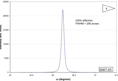
Figure 3.9 X-ray diffraction scan of undoped GaN: (002) reflection, (b) (004) reflection, and (c) (006) reflection………..…49
Figure 3.11 X-ray diffraction scan of undoped GaN: (006) reflection……….50
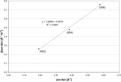
Figure 3.12 Williamson-Hall plot of undoped GaN………..51
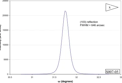
Figure 3.13 X-ray diffraction scan of undoped GaN: (103) reflection…….…………52
Figure 3.14 X-ray diffraction scan of undoped GaN: (302) reflection………...……..53
Figure 3.15 Plot of crystal quality characteristics of a series of GaN films……..……56
Figure 3.16 Photoluminescence of optimized undoped GaN………....58
Figure 3.17 Silane dilution manifold………...60
Figure 3.18 Mobility and carrier concentration vs. silane flow for n-type GaN…...…61
Figure 3.19 Photoluminescence of n-type GaN………..………..62
Figure 3.20 AFM image of n-type GaN surface………..….64
Figure 3.21 PL spectra of annealed and unannealed p-type GaN with
p = 2.22x1017 cm-3……….…70
Figure 3.22 PL spectra of annealed and unannealed p-type GaN with
p = 6.73x1017 cm-3………....….71
Figure 3.23 Simplified band diagram of Mg-doped GaN, showing optical
transitions at 387 nm and 428 nm………..…72
Figure 4.1 InGaN/GaN double heterostructure………...………80
Figure 4.2 Equilibrium vapor pressures of common compound semiconductors…...82
Figure 4.3 Reaction pathways for the deposition of In-based nitride compounds…..85
Figure 4.4 Band-bending in a double heterostructure……….…88
Figure 4.5 Binodal (solid) and spinodal (dashed) curves for the InGaN system……90
Figure 4.6 Emission wavelength vs. In/Ga ratio for samples grown at 875ºC…..…..89
Figure 4.7 Emission wavelength vs. growth temperature for a series of
Figure 4.9 ω-2θ x-ray scan of a series of capped 4-well InGaN/GaN
structures, measured at the (a) center; and (b) tip ………...98
Figure 4.10 Growth rate vs. growth temperature for capped InGaN/GaN
structures, measured at the center………...……….100
Figure 4.11 Growth rate vs. growth temperature for capped InGaN/GaN
structures, measured at the tip………..………101
Figure 4.12 TEM images of a capped 4-well MQW structure at (a)160kX
magnification; and (b) 200kX magnification………...102
Figure 4.13 Emission wavelength vs.growth temperature for InGaN/GaN
quantum well structures capped at 975ºC ……….………..103
Figure 4.14 FWHM of emission peak vs. growth temperature for InGaN/GaN
quantum well structures capped at 975ºC ………...104
Figure 4.15 Emission wavelength vs. quantum well growth time for InGaN/GaN quantum well structures capped at 975ºC………....105
Figure 4.16 Emission wavelength vs. TMG flux for InGaN/GaN
quantum well structures capped at 975ºC………....107
Figure 4.17 PL emission spectra obtained by capped InGaN/GaN structures grown
using the TSS-CCS………..108
Figure 4.18 Example of non-uniform emission in an InGaN/GaN QW structure…..111
Figure 4.19 (a) Top and (b) side views of reactor’s PBN-coated graphite heater...…112
Figure 4.20 Example of improved emission uniformity in an InGaN/GaN
structure due to reduced temperature ramp rate………..……….113
Figure 4.21 PL emission spectra obtained by capped InGaN/GaN structures
on wedge-shaped substrates……….115
Figure 4.22 Photos of capped InGaN/GaN QW samples with metallic
appearances………..116
Figure 4.23 Degraded emission characteristics from metallic InGaN/GaN
structure………117
Figure 5.1 Emission wavelength vs. indium content for relaxed and
strained InGaN ………....128
Figure 5.2 Calculation of the Szmulowicz formulation of the Kronig-Penney model for a 16% InGaN/GaN QW structure for (a) the conduction
band and (b) the valence band……….131
Figure 5.3 Bandgap shift due to quantum size effect vs. In content for various
length quantum wells………...132
Figure 5.4 Electric field [from both spontaneous and piezoelectric polarization]
vs. In content………135
Figure 5.5 Emission wavelength vs. In content for various length quantum wells...138
Figure 5.6 Electron and hole envelope functions for (a) an unstrained
quantum well, and (b) a compressively strained quantum well………...140
Figure 5.7 Comparison of emission spectra of 35Å and 44Å quantum-well
structures………..141
Figure 6.1 CIE Chromaticity diagram showing Illuminant D65……….…...147
Figure 6.2 CIE Color-matching functions from 1931 and 1978………...148
Figure 6.3 White LED structure using red, green, and blue active regions………..151
Figure 6.4 Change in color coordinates vs. fractional flux variation………152
Figure 6.5 White LED structure using violet and yellow active regions…………..153
Figure 6.6 CIE chromaticity diagram showing two complementary wavelengths
combining to make white light at Illuminant D65………154
Figure 6.7 I-V characteristic of p-n junction……….157
Figure 6.8 Ideality factor plot for p-n junction………..159
Figure 6.9 Electroluminescence spectra of green LED under high
injection current ………..161
Figure 6.10 Electroluminescence spectra of green LED under low
Figure 6.11 Electroluminescence spectra of yellow/amber LED under high
injection current ………..………163
Figure 6.12 Electroluminescence spectra of yellow/amber LED underlow
injection current……….………..………164
Figure 6.13 Photographs of LED #S069-06 operating at (a)10 mA and (b) 2mA…..165
Figure 6.14 PL spectra of yellow-emitting device structure………...166
Figure 6.15 Calculated values of electron-hole pair concentration for
a series of ND-filtered laser beams………..168
Figure 6.16 Calculated values of electron-hole pair concentration for
a series of injection currents………169
Figure 6.17 I-V Characteristics of yellow and green devices……….170
Figure 6.18 Ideality factor plots for yellow and green devices………...171
Figure 6.19 PL emission spectra of white-emitting devices composed
of 2x2 QW’s……….174
Figure 6.20 PL emission spectra of white-emitting devices composed
of 3x3 QW’s……….………174
Figure 6.21 PL emission spectra of white-emitting devices composed
of 4x4 QW’s……….175
1.0 General Background
1.1 A Brief History of Electric Light
On October 21, 1879, the world was witness to one of the most significant events
in the history of invention. A man named Thomas Alva Edison, also known as “The
Wizard of Menlo Park,” demonstrated the world’s first incandescent light bulb [1].
Composed of a carbon filament sealed under vacuum in a glass housing, this rudimentary
photon source had a lifetime of forty hours and demonstrated to the world that
electric-powered lighting was now a reality.
To this day, Edison’s incandescent bulb (now generally containing an iodized
tungsten filament) remains in widespread use. The fluorescent light, conceived by
Nikolai Tesla and introduced by the Westinghouse Electric Company in 1939 [2], is also
a common electrical lighting source. However, a promising new technology is quickly
emerging which may soon make both incandescent and fluorescent lights obsolete. This
technology, referred to as solid-state lighting, uses semiconductor-based devices to
transform electrical power into emitted photons.
The fundamental principles of solid-state lighting are fairly straightforward. In a
semiconductor with bandgap Eg, recombination of an electron-hole pair (EHP) leads to
the release of an amount of energy equal to Eg. One way this energy can be released is
through emission of a photon. The wavelength, λ, of this emitted photon is governed by
the bandgap of the semiconductor material according to λ =hc/Eg. Thus, a light source of
a desired wavelength can be engineered by using a semiconductor with the proper
The first serious research regarding solid-state lighting occurred in the early
1960’s. It was known at this time that a forward-biased GaAs p-n junction would emit
infrared radiation. GE’s Nick Holonyak took this technology a step further by alloying
GaAs with GaP, thus creating a material that emitted red light when a current was passed
through it [3]. Devices were fabricated from this material, and thus the world’s first light
emitting diode (LED) was introduced.
Since the arrival of Holonyak’s first LED, the advances in this area have been
tremendous. Not only has Holonyak’s red been improved, but the entire visible spectrum
is now available. Figure 1.1 shows the rapid improvement in luminous efficiency as time
has passed and more dollars and man-hours have been spent studying the phenomenon of
solid-state lighting. An approximate ten-fold improvement per decade can be seen.
1.2 The Measurement of Light
In order to fully understand solid-state lighting, one must first become familiar
with the way in which the physical properties of light are measured. Generally,
electromagnetic radiation is characterized by radiometric quantities, such as number of
photons, photon energy, and radiant flux [5].
The use of radiometric units, however, can be somewhat misleading when trying
to measure visible lighting. This is because the human eye does not sense all
wavelengths of light equally. Sensitivity is maximized near the center of the visible
spectrum (555 nm) and tails off in either direction. This is demonstrated in Figure 1.2,
which shows eye sensitivity as a function of wavelength.
Figure 1.2 Relative sensitivity of human eye to visible wavelength [6]
Radiometric units do not take this sensitivity dependence into account. In fact,
ultraviolet, etc.) radiation. Thus, the use of radiometric quantities for visible light sources
is far from ideal.
For this reason, photometric quantities have been introduced. Photometric
quantities are used to characterize light according to the sensitivity of the human eye [5].
An example is the luminous flux, which represents the light power of a source as
perceived by the human eye. Luminous flux is measured in units of lumen (lm).
Another important photometric quantity is luminous efficacy—the luminous flux
per unit power measured in units of lumens/watt. It is related to quantum efficiency, but
there is an important distinction between the two. Whereas quantum efficiency simply
measures the electron-to-photon conversion capability of the light source, the luminous
efficacy weights the light output as per the photopic response of the human eye [7].
For example, typical blue LED’s have a much higher quantum efficiency (60%)
than do green LED’s (20%) [8]. However, because of each color’s location on the eye
sensitivity chart (Figure 1.2), the typical luminous efficacy of green LED’s is three times
higher than that of blue LED’s (~ 30 to 10 lumens/watt) [9].
1.3 Advantages of LED’s
The next issue is to examine what advantages LED’s have over standard (i.e.,
incandescent and fluorescent) lighting sources. As with any new technology, a solid
argument must be made as to why, and in what ways, the new product is superior to the
existing product.
The first major advantage of solid-state lighting is lifetime. By some estimates,
advantage is particularly attractive for applications where bulb replacement is especially
difficult or impossible.
The ruggedness of LED’s is also an asset. An incandescent or fluorescent light
can be shattered or crushed, and if an incandescent bulb is dropped, even if the glass
remains intact, one may find the filament has broken. LED’s, on the other hand, can
handle such shock and still operate properly. LED’s are also much more resistant to
vibration than their incandescent counterparts.
Perhaps the greatest advantage of LED’s, however, is their superior efficacy.
Incandescent bulbs are inherently inefficient, due to the fact that 72% of their emitted
radiation is in the infrared range [10]. This leads to typical efficacy values of 15-20
lumens/watt [8], numbers which, given the maturity of the technology, will not be
increasing much, if at all. Using a filter on an incandescent bulb to create a
monochromatic (single-color) light reduces the efficacy even more (12 lm/W for yellow,
5 lm/W for red).
MonochromaticLED’s, on the other hand, are currently being manufactured with
efficacies several times higher (see Table 1.1). Also bear in mind that solid-state lighting
technology is still in its early stages. As more research is needed into the growth and
Table 1.1 Top efficacies of single-color LED’s currently in production [8]
Color Efficacy
(lumens/watt) Manufacturer
Material system
Red 42 Lumileds Phosphide
Red-orange 53 Lumileds Phosphide
Orange 18-22 Toshiba Phosphide
Yellow 34-35 Lumileds Phosphide
Yellow-green 8 P. Tec Opto Phosphide
Green 25-32 Nichia Nitride
Blue-Green 25-28 Nichia Nitride
Blue 9-12 Cree Nitride
Of course, these improvements in efficacy will lead to a decrease in energy
consumption as LED’s gradually replace incandescent sources for many, if not all,
applications. The U.S. Department of Energy predicts that, by the year 2020, the use of
SSL will lead to a savings of at least 18 terrawatt-hours (TWh). Note that this value was
obtained using their most conservative (base-case) estimates; more ambitious models call
for a potential savings of up to 246 TWh [11].
This decrease in energy consumption will lead to a subsequent decrease in carbon
emission from power plants, which has obvious environmental benefits. The base-case
calculations estimate a decrease of 3.16x10⁶ metric tons of carbon by 2020, while the
more optimistic models claim the reduction could be an order of magnitude higher
The advantages discussed in this section are why LED’s are rapidly replacing
their peers in lighting applications all around the industrialized world. It seems
everything from advertising displays to traffic signals, we are seeing the emergence of
solid-state lighting. This fact hit home just recently when my eight-year old neighbor,
Ethan, proudly showed me his new sneakers. His favorite feature was – to my
amusement – a series of red LED’s than lit up every time he took a step.
1.3 White Light using LED’s?
As ubiquitous as single-color LED’s have become, we have really only just seen
the beginning of how solid-state lighting can enhance our lives. The real revolution in
lighting technology will occur if (when?) we are able to replace our conventional white
light source with LED’s.
The most straightforward way to generate white light is to simply combine
monochromatic light of the three primary colors: red, green, and blue (RGB). This will
produce a white source matching the RGB sensors of the human eye [12]. This is often
demonstrated by the 1979 CIE (Commission International de l’Eclairage) chromaticity
Figure 1.3 CIE Chromaticity Diagram (1976) [13]
The axes of the chromaticity diagram (u', v') are referred to as the uniform
chromaticity coordinates, and are a representation of the relative stimulation of the
human eye to the three primary colors. The points of the perimeter of the diagram
represent saturated colors, meaning those which consist of a single wavelength [5].
(Note the white dots labeled in 10 nm increments.) Such a color would appear as a single
vertical line on an intensity vs. wavelength plot (i.e., a photoluminescence measurement).
A broadening of this line would correspond to the point on the edge chromaticity diagram
moving inward toward the center. Continued broadening will lead a wide spectrum
which is composed of all colors (i.e. white light), which is found in the center of the
diagram.
When examining the white region of the chromaticity diagram, one may notice a
Planckian locus, because it indicates the coordinates of the light given off by a blackbody
emitter as its temperature is increased. If LED-generated white light is to be sufficient
quality, it must fall upon this line [14].
The position along the locus is quantified by the parameter known as correlated
color temperature (CCT). Its physical definition is the temperature at which a black body
must be heated in order to emit the given color of light [15]. Candlelight, for example,
has a relatively low CCT of 1500K, and thus appears reddish-orange in color.
Incandescent and fluorescent lights operate at a CCT of around 2500-3500K; this is a
reasonable target for white LED’s.
Another important parameter for measuring the quality of electric light is the
color-rendering index, Ra. It is defined as the ability of an illumination source to render
true colors [15]. Its values are given on a scale of 0-100. The mid-day sun has Ra≈100,
as do most incandescent bulbs. White LED’s should posses an Ra of at least 75 for use in
indoor lighting. However for some applications, such as outdoor streetlights, a lower
color-rendering index (Ra≈40) is acceptable.
The question now becomes: is it possible to create white light of sufficient quality
through solid-state technology? The answer, at first glance, appears to be affirmative.
Currently, the technology exists to manufacture LED’s whose colors span the entire
visible spectrum. It should then simply be a matter of putting the three primary colors
(red, green, and blue) in one device and thus have a white LED.
Of course, this task is not as simple as it sounds. Currently, long wavelength
(red-yellow) LED’s are manufactured with the gallium phosphide family of materials
lattice incompatibilities, it is not possible to incorporate both materials into the same
device. Our study must therefore begin with the choice of the appropriate material.
1.4 Potential of the Gallium Nitride Material System for Solid-State Lighting
When one looks to the materials that can potentially be used in the fabrication of
white LED’s, the compound semiconductor gallium nitride (GaN) emerges as a
candidate. First of all, GaN is a direct bandgap material (see Figure 1.4), which means
that electron-hole pairs will combine radiatively, i.e. through photon emission. This is in
contrast to indirect bandgap materials, in which recombination tends to be non-radiative.
Figure 1.4 E-k diagram of gallium nitride [18]
Another positive aspect of GaN is that it can be alloyed with related compounds
aluminum nitride and/or indium nitride to form ternary compounds AlGaN and InGaN, or
the quaternary compound AlInGaN. Starting with the binary GaN (Eg = 3.4 eV), one can
controlled fashion. As shown in Figure 1.5, the GaN material system can thus be used to
cover a very broad range of bandgap values (0.7 - 6.1 eV), and thus a wide span of
emission wavelengths (200 – 1378 nm) that covers nearly of the visible spectrum. Use of
the quaternary material, AlInGaN, has the added advantage of giving one the ability to
independently control both bandgap and lattice parameter [19].
Figure 1.5 Bandgap vs. lattice constant for nitride material system [20]
The ability of the ternary compound InGaN to push the emission wavelength of
GaN into the visible range is a very advantageous property of this material system.
Through use of a series of InGaN alloys, each with an increasing value of In content, it
appears feasible to fabricate blue, green, and red emission on the same chip (i.e., a white
LED). Thus, this study will focus on the use of InGaN as its active layer in all device
It is also important to note that all of the GaN-based alloys that have been
discussed (InGaN, AlGaN, and AlInGaN) have direct bandgaps over their entire
composition range. This is in contrast to the aforementioned AlxInyGa1-x-yP system (see
Section 1.2), which converts to an indirect bandgap for Eg > 2.33 eV (which corresponds
to λ=532 nm, i.e. green emission) [21]. For this reason the phosphide system is not a
viable candidate for monolithic white LED’s.
Thus far the discussion of solid-state white lighting has focused on the placement
of three active regions, one for each primary color, on a single chip. There is, however,
another way in which LED’s can be used as a white light source. It involves the use of a
single short-wavelength (UV or blue) device coated with an epoxy containing one or
more phosphors [22]. The purpose of the phosphor(s) is to absorb the high-energy
photons from the LED and convert them to longer wavelengths. This method has proven
very successful through use of nitride-based LED’s and rare-earth ion (Ce+ [23] or Eu+
[24]) based phosphors.
This technique, however, suffers from a few major drawbacks. First, there is an
inherent inefficiency present in these sources due to the conversion of high-energy blue
or UV photons to low-energy yellow or red. Also, the lifetimes of these LED’s are
shortened by the yellowing of the epoxy with holds the phosphors, which is attributed to
both photodegradation and ohmic heating at the p-n junction [25]. Therefore, it is
certainly beneficial to explore the possibility of the three-color InGaN device described
previously, as such device would circumvent both of the major problems seen in
The following chapters in this dissertation are broken down as follows: Chapter 2
explains the fundamentals of metal-organic vapor deposition (MOCVD), which is the
film growth technique used in this study. Chapter 3 provides the necessary background
information behind the study of GaN, and presents the preliminary GaN growth data. N-
and p-type doping are also discussed. Chapter 4 explains the fundamental challenges
related to InGaN growth, then provides the experimental results of our InGaN growth
study. Chapter 5 focuses the calculation of emission wavelength from InGaN-based
structures, while Chapter 6 presents long-wavelength device results as well as a
demonstration of white emission. The dissertation concludes with Chapter 7, which
1.7 References
1. T. A. Edison. U.S. Patent No. 223,898 (1880).
2. Twenty First Century Books, an online Tesla information resource: http://www.tfcbooks.com/teslafaq/q&a_028.htm
3. N. Holonyak, Jr. and S.F. Bevacqua. “Coherent (visible) light emission from Ga(As1-xPx) junctions.” Appl. Phys. Lett.1, 82 (1962).
4. M. Krames. “Progress and future direction of LED technology.” SSL Conference Presentation. Arlington, VA. (2003).
5. E.F. Schubert. Light-Emitting Diodes, Chapter 11.2. Cambridge University Press,
Cambridge (2003).
6. P.K. Kaiser. The Joy of Visual Perception: A Web Book. Found online at
http://www.yorku.ca/eye/photopik.htm
7. D.A. Kirkpatrick. “Is solid-state the future of lighting?” Proc. of the SPIE Vol. 5187: Third Internat’l. Conf. on Solid-State Lighting. I.T. Ferguson, N. Narendran, S.P.
Denbaars, J.C. Carrano, eds. (2003).
8. M.G. Craford. “Visible light emitting diodes: past, present and a very bright future.”
MRS Bull.25 (10), 27 (2000).
9. D.L. Kleipstein. The Brightest and Most Efficient LED’s and Where to Get Them. Found online at http://members.misty.com/don/led.html
10. S.H. Lydecker, K.F. Leadford, C.A. Ooyen. “Lighting industry acceptance of solid state lighting.” Proc. of the SPIE Vol. 5187: Third Internat’l. Conf. on Solid-State Lighting. I.T. Ferguson, N. Narendran, S.P. Denbaars, J.C. Carrano, eds. (2003).
11. M. Kendall and M. Scholand. “Energy savings potential of solid state lighting in general lighting applications.” Final report prepared by Arthur D. Little, Inc. for the U.S. Department of Energy (2001).
12. D.A. Steigerwald, J.C. Bhat, D. Collins, R.M. Fletcher, M.O. Holcomb and M.J. Ludowise. “Illumination with solid state lighting technology.” IEEE J. on Sel. Top. in Quant. Elec.8, 310 (2002).
13. Ledtronics, Inc. homepage. Found online at
14. S. Muthu. “Red, green, and blue LEDs for white light illumination.” IEEE J. on Sel. Top. in Quant. Elec.8, 333 (2002).
15. Lighting Design Glossary. Found online at http://www.schorsh.com/kbase/glossary/
16. F.A. Kish and R.M. Fletcher. “AlInGaP Light-Emitting Diodes.” Semiconductors and Semimetals, Vol. 48: High Brightness Light-Emitting Diodes. G.B. Stringfellow
and M.G. Craford, eds. Academic Press, San Diego (1997).
17. S. Nakamura, S. Pearton and G. Fasol. The Blue Laser Diode: The Complete Story,
Chapters 9 and 10. Springer, Berlin (2000).
18. Ioffe Physico-Technical Institute electronic archive: Physical properties of semiconductors. Found online at
http://www.ioffe.rssi.ru/SVA/NSM/Semicond/index.html. Diagram is adapted from M. Suzuki, T. Uenoyama and A. Yanase. “First principles calculations of effective-mass parameters of AlN and GaN.” Phys. Rev. B. 52, 8132 (1995).
19. M.E. Aumer, S.F. LeBoeuf, F.G. McIntosh, and S.M. Bedair. “High optical quality AlInGaN by metalorganic chemical vapor deposition.” Appl. Phys. Lett.75, 3315
(1999).
20. EMF Limited homepage. Found online at http://www.emf.co.uk/
21. C.H. Chen, S.A. Stockman, M.J. Peanasky and C.P.Cuo. “OMVPE of AlGaInP for high-efficiency visible light-emitting Diodes.” Semiconductors and Semimetals, Vol. 48: High Brightness Light-Emitting Diodes. G.B. Stringfellow and M.G. Craford,
eds. Academic Press, San Diego (1997).
22. R. Mueller-Mach, G.O Mueller, M.R. Krames, and T. Trottier. “High-power
phosphor-converted light-emitting diodes based on III-nitrides.” IEEE J. on Selected Topics in Quant. Elec. 8, 339 (2002).
23. J.L. Wu, S.P. Denbaars, V. Srdanov, H. Weinberg. “Cerium doped garnet phosphors for application in white GaN-based LEDs.” Materials Research Society Proceedings Vol. 667: Luminescence and Luminescent Materials Symposium, p G5.1.1 (1999).
24. J.K. Park, M.A. Lim, J.T. Park, S.Y. Choi. “White light-emitting diodes of GaN-based Sr2SiO4:Eu and the luminescent properties.” Appl. Phys. Lett.82, 683 (2003).
2.0 Metal-Organic Chemical Vapor Deposition
2.1 Introduction to MOCVD
As discussed in the previous chapter, the GaN material system has been shown to
be excellent candidate for solid-state lighting. The next step, therefore, is to determine
the technique through which the GaN-based devices can be manufactured. For this
particularly study, metal-organic chemical vapor deposition (MOCVD) has been chosen.
Metal-organic chemical vapor deposition (MOCVD) is a thin-film growth
technique which involves the flow of gaseous precursors (usually, as the name implies,
metal-organics) into a reaction chamber, which will contain a heated substrate. When the
precursors reach this substrate, they are “cracked” (i.e., decomposed), which leads to a
series of chemical reactions between the reactive species created by the cracking process.
The result of these reactions is the deposition of a thin film on the substrate.
The flow of metal-organic is achieved by passing a carrier gas (usually hydrogen,
nitrogen, or some mixture of the two) through a bubbler containing the metal-organic in
either liquid or solid form. The molar quantity of metal-organic compound entering the
chamber is governed by the bubbler temperature, bubbler pressure, and the flow rate of
carrier gas through the bubbler.
The basic building blocks for MOCVD-growth of gallium nitride are
well-defined. The most common gallium source (and the one used in this dissertation) is
trimethylgallium (TMG), which is readily available from several vendors. There is also
some interest in the use of triethylgallium (TEG), which has a much lower vapor pressure
than TMG. Some studies have shown that GaN films grown with TEG tend to contain
The vast majority of GaN studies, including this one, favor the use of ammonia
(NH3) as a nitrogen source. Its cracking efficiency is low at typical GaN growth
temperatures (~1000˚C), so relatively large amounts of NH3 must be used for sufficient
quality GaN growth (typical molar NH3/TMG ratios ≈ 1000-3000). Dimethylhydrazine
(DMHz), a nitrogen-containing organometallic, has also been experimented with as a
nitrogen source [3], as has hydrazoic acid (HN3) [4].
The carrier gas used in this study was nitrogen. This is in contrast to most current
MOCVD systems, in which hydrogen is used as a carrier. Hydrogen was introduced
independently into the reactor in most cases, due to its beneficial thermal conductivity
and carbon-radical scouring properties. However, there are certain instances (InGaN
growth, for example) in which the presence of hydrogen is detrimental to the growth (see
Chapter 4). Our growth system affords us the opportunity to completely eliminate the
flow of hydrogen into the reactor when desired, which can be a major advantage when
growing InGaN-based structures.
2.2 Thomas Swan Scientific MOCVD System
All samples studied in this body of work were grown by an Epitor MOCVD
system manufactured by Thomas Swan Scientific Equipment Ltd (Swavesey, Cambridge,
Mass flow controller
Valve
Pressure controller
Organometallic bubbler
SiH4
NH3
H2
N2 supply
Exhaust
TMG TMI
Reactor
Make-up lines
Upper Run Line (Column V) Lower Run Line (Column III)
H2
Cp2Mg
Make-up lines
Upper Vent
Lower Vent
Figure 2.1 Diagram of Thomas Swan MOCVD gas delivery circuit
The main components of the gas delivery manifold are the carrier gas supply,
upper/lower vent lines, upper/lower run lines, make-up lines, organometallic (OM)
bubblers, and gaseous reactant sources. The appropriate materials will flow from this
circuit into a reactor, where the film growth will take place. Reactor designs will be
discussed in detail in Section 2.3.
The description of system operation starts with the carrier gas. As can be seen in
Fig. 2.1, the carrier gas is introduced into the manifold upstream of all the other
designed in such a way that either hydrogen or nitrogen can be used as a carrier gas; in
the present work it is nitrogen.
Since the carrier gas is used ubiquitously in system processes, its purity is of
obvious importance. For this reason, a Nanochem 1400 resin purifier was used to reduce
contaminants in the carrier N2. Monitoring the purity of the carrier N2 was carried out by
a Panametrics hygrometer. Throughout all processes described herein, the dewpoint
reading remained below the detectable range of the hygrometer (-110°C), which
corresponds to an H2O concentration less than 2 ppm.
The carrier gas flows through the upper (column III) and lower (column V) run
lines, carrying all reactants present in these run lines into the reactor. The use of two
separate run lines is essential because the OM sources used as column III precursors are
Lewis acids; whereas ammonia, the primary column V source, is basic [5]. Therefore
any pre-mixing between the two will lead to gas-phase reactions which are detrimental to
the film growth process. Also, it is important, when performing growth, to ensure that
the total flow through each run line is properly balanced; otherwise backstreaming into
the lower-flow line may occur.
Coupled with each run line is a corresponding vent line. These vent lines are
simply paths through which a reactant flow can be diverted if it is not, at that particular
time, desired in the reactor. Further downstream, the two vent lines combine and then
pass through a pyrolysis furnace, which decomposes any potentially hazardous OM’s
before they are released to the exhaust.
The precursors themselves are either from a gaseous source (as in the case of H2,
sources are simply fed into the delivery manifold from a remote high-pressure tank. The
OM precursors are held in temperature- and pressure-controlled bubblers, through which
the carrier gas travels when an OM flow is needed. The molar quantity of OM “picked
up” and sent into the run lines (and subsequently the reactor) is governed by the bubbler
temperature, bubbler pressure, and carrier gas flow rate.
One of the novel aspects of the Thomas Swan deposition system is its utilization
of make-up lines. The purpose of these lines is to eliminate any variation in flow through
the run lines which may result from the switching of reactant flows from the run line to
the vent (and vice-versa). Such perturbations can lead to rough interfaces between
epitaxial layers, which are unacceptable when dealing with the nanometer-range features
of modern semiconductor device structures.
The flow rate and pneumatic switching of these make-up lines are controlled by
the TSS system software, which anticipates run-line fluctuations (due to run/vent
switching) and eliminates them by flowing the appropriate amount of N2 (or H2) through
the make-up lines. The flow from the make-up line compensates for the sudden loss (or
gain) of flow that results from switching a reactant stream from the run line to the vent
line (or vice-versa). Thus, the reactor experiences a uniform, unperturbed flow despite
the switching of reactants and the corresponding epitaxial interface will be appropriately
sharp.
2.3 MOCVD reactors
Of course,in addition to the gas manifold, another important set of design criteria
to heat the substrate to temperatures greater than 1000°C, rotate the substrate (to reduce
boundary layer thickness), and be non-reactive.
2.3.1 Early reactor design
The first reactor used for the growth of gallium nitride was a “home-made”
chamber designed and constructed in our lab. A drawing of this reactor is given in Figure
2.2.
Thermocouple RF coils
) Gas inlet tube
Two-piece susceptor
Rotation arm
Exhaust
Figure 2.2 Original GaN reactor design [6]
Work with this reactor, however, never yielded any material of sufficient quality.
There were several recurrent problems, such as poor film surfaces, low (<80 cm2/V-sec)
mobilities, and emission dominated by deep levels. A series of minor modifications were
made to this reactor in an attempt to address these problems, but none of the changes led
There are a litany of problems inherent in this particular system design which led
to the repeated poor-quality films. These issues are discussed as follows:
• Gas phase reactions – Due to the relatively large distance (>100 mm) between the
inlet and susceptor, the ammonia and metalorganics would meet well above the
growth surface. As mentioned previously, this leads to an acid-base pre-reaction
which is detrimental to film growth.
• Recirculation pockets – Another design flaw with this reactor was the dead
volume above the susceptor to the right and left of the sample. At high process
temperatures, thermal buoyancy likely lead to recirculating air pockets in these
areas. These disturbances can disrupt the laminar flow of the reactant gas stream
over the substrate surface, leading to poor film quality.
• Jetting – As can seen in the figure, the reactor featured a small inlet tube injecting
gases into much larger volume. This leads to the phenomenon of jetting, wherein
the inlet gases rapidly expand to fill the open volume. This phenomenon also
leads to perturbations in the laminar flow, and negatively affects film growth.
• Exposure of chamber to atmosphere – Since there was no load-locked glovebox in
this setup, the interior of the reactor was exposed to atmosphere every time a
sample was loaded or unloaded. This may have lead to the presence of residual
water vapor in the reactor during growth, even after the pre-growth cycle purge.
Also, post-growth exposure of the reactor to atmosphere could have potentially
led to reactions (i.e., oxide formation) with the metals deposited on the on the
wall after growth. This is particularly troublesome when working with Al- or
2.3.2 Thomas Swan Scientific close-coupled showerhead reactor [7]
Due to the problems with the above reactor, it became necessary to take a new
approach. It was decide the best course of action was to purchase the close-coupled
showerhead (CCS) reactor designed and manufactured by Thomas Swan Scientific. This
reactor was then fully installed by the author. A diagram is shown in Figure 2.3.
Figure 2.3 Thomas Swan Scientific close-coupled showerhead (TSS-CCS) reactor [8]
The TSS-CCS is a vertical, axially symmetric rotating disc reactor [9] based on
the stagnation-point concept [10]. The chamber itself is stainless steel, with a removable
quartz inner-liner to prevent deposition on the interior walls. The input gases are
introduced laterally into the chamber and delivered to the substrate via TSS’s patented
showerhead. The substrate sits on a silicon carbide-coated graphite susceptor, which is
heated resistively, and rotated via a FerrofluidicTM [11] double magnetic fluid/bearing
Perhaps the most significant benefit of this reactor is the close proximity of the
susceptor to the gas inlet (~2 cm). This leads to a reduced residence time of the reactants
over the substrate, which (a) helps to prevent gas-phase reactions between column III
metalorganics and ammonia; and (b) leads to enhanced interface abruptness. Another
advantage of this design is that it results in a very small volume above the susceptor,
which minimizes the formation of re-circulating gas pockets. It is also important to note
that, despite this short length, the reactants are believed to be fully mixed when they
reach the susceptor. This assessment has been verified by mathematical analysis [12].
The showerhead itself (shown in Figure 2.4) is another one of the major benefits
of this reactor. It is composed of a very high-density (~100 tubes/in2) set of inlet tubes,
with every-other tube being either column III or column V. The size of the showerhead
is matched to the size of the susceptor (in this case, 2 in. diameter). Such a design
provides a number of advantages over the smaller inlet tube discussed earlier.
Figure 2.4 Photo of Showerhead [4]
The first such advantage is uniformity. The showerhead introduces a
a small area. This eliminates “shadowing” effects, this leading to a uniform thickness
profile as well as uniform dopant incorporation and alloy composition, where applicable.
This well-controlled inlet technique also helps ensure run-to-run reproducibility.
Another advantage of the showerhead design is the elimination of jetting. As
discussed in the previous section, jetting is the phenomenon in which the incoming gases
must expand rapidly to fill the reactor volume, thus disrupting the laminar flow. This
occurs commonly in reactors where the inlet gases are fed into the chamber by a small
tube (see Figure 2.2). The showerhead, on the other hand, provides a diffuse introduction
of reactants, therefore jetting is avoided.
The substrate heating in this reactor is achieved through a resistive heater made of
pyrolytic boron nitride-coated graphite. In order to eliminate dead volume in the space
around the heater, the system is equipped with a heater purge line. Initially, 200 sccm of
nitrogen was sent through this line during all growth and baking steps. However, due to
heater lifetime issues, the flow rate and gas species of this purge needed to be adapted. As
per the recommendation of TSS, the heater purge was increased to 600 sccm of hydrogen.
No significant, measurable changes in film properties were noticed due to this alteration.
During all processes, temperature is controlled by a type-C thermocouple placed
on the underside of the susceptor, which communicates with a Eurotherm 818
temperature controller. Because of its location, however, the thermocouple does not give
a true reading of substrate surface temperature. Thus, an actual temperature vs.
thermocouple temperature calibration curve is needed.
Actual surface temperature measurements were obtained in the TSS-CCS reactor
fitted into the ports and connected via fiber optic cable to a Mikron M668 optical
pyrometer, which provided an actual surface temperature (Tact) reading. The light guides,
cable, and pyrometer were calibrated using an Instron SFL black body furnace. The
graphite susceptor was assumed to have an emissivity of 1.0.
Calibration was thus carried out by mimicking the gas-flow parameters for each
of the three temperature regimes (buffer layer growth, InGaN growth, and GaN
growth/bakeout) and taking a series of actual surface temperature (Tact) readings using a
Mikron M668 optical pyrometer. These values were then plotted vs. the corresponding
thermocouple temperature (TTC) readings.
Figure 2.5 gives these calibration curves for the two different heater purge
conditions used in this study. Note that the values of TTC and Tact match much more
closely when hydrogen is used as a purge gas, i.e., in the GaN growth regimes of Figure
2(b). This is because the higher thermal conductivity of H2 leads to better
500 600 700 800 900 1000 1100
500 600 700 800 900 1000 1100 1200 1300
thermocouple readout (C)
py
romet
er te
mp
era
tu
re (C)
a)
500 600 700 800 900 1000 1100
500 600 700 800 900 1000 1100 1200 1300
thermocouple readout (ºC)
pyromete
r t
emper
ature
(º
C)
b)
Figure 2.5 TSS-CCS temperature calibration for (a) 300 sccm N2 purge; and (b) 600
It is important to note that all of the growth temperature values reported in this
study are actual substrate surface temperatures (Tact) as per this calibration.
The final major improvement of the TSS-CCS reactor is the presence of a
nitrogen-purged glovebox and attached load-lock. These features make it possible to
load and unload samples with exposing the interior of the reactor to atmosphere. This
will reduce the residual oxygen and water vapor in the chamber during growth and help
prevent the formation of oxides which may result from the presence of post-growth
2.4 References
1. Saxler, D.Walker, P. Kung, X. Zhang, M. Razeghi, J. Solomon, W.C. Mitchel, H.R. Vydyanath. “Comparison of trimethylgallium and triethylgallium for the growth of GaN.” Appl. Phys. Lett.71, 3272 (1995).
2. J.S. Park, Z.J. Reitmeier, R.F. Davis. “Comparison of the microstructure and chemistry of GaN (0001) films grown using trimethylgallium and triethylgallium on AlN/SiC substrates.” Phys. Stat. Sol.(c)2, 2166 (2005)
3. E.D. Bourrett-Courchesne, Kin-Man Yu, S.J.C. Irvine, A. Stafford, S.A. Rushworth, L.M. Smith, R. Kanjolia. “MOCVD of GaN on sapphire using the alternate precursor 1,1-dimethylhydrazine.” J. of Crys. Gr.221, 246 (2000).
4. H. Sato, H. Takahashi, A. Watanabe, and H. Ota. “Preparation of GaN films on sapphire by metalorganic chemical vapor deposition using dimethylhydrazine as nitrogen source.” Appl. Phys. Lett. 68, 3617 (1996).
5. R.H. Moss and J.S. Evans. “A new approach to MOCVD of indium phosphide and gallium-indium arsenide.” J. of Cryst. Gr.55, 129 (1981).
6. S.F. LeBoeuf. “Manipulating two-dimensional electron gas properties in III-V nitrides via AlInGaN strain engineering.” Ph.D Thesis. North Carolina State University (2001).
7. E.J. Thrush. M. Kappers, L. Considine, J.T. Mullins, V. Saywell, F.C. Bentham, N.Sharma, C.J. Humphreys. “Close coupled showerhead reactors for the growth of group III nitrides.” Proc. China-Japan workshop Nitride Semiconductor Materials and devices, p. 119. CJWN, Shanghai (2001).
8. Thomas Swan Scientific Equipment CCS-MOCVD Reactor System Manual – CS62912, Issue 1.1. Technical Author: Trevor Webb (1999).
9. K.F. Jensen. “Transport phenomena in vapor phase epitaxy reactors.” in Handbook of Crystal Growth 3, Thin Films and Epitaxy, Part B: Growth Mechanisms and
Dynamics, p 541. D.T.J. Hurle, ed. North Holland Publishing (1994).
10. N.A.V. Piercy. Aerodynamics, Chapter II.32. D. Van Nostrand Company, Inc., New
York (1937).
11. “Ferrofluidic” is a registered trademark of Ferrotec (USA) Corporation. A technical description of how such a bearing operates can be found at
3.0 Fundamentals of Gallium Nitride
3.1 Crystallography of Gallium Nitride
There are two allotropes of gallium nitride: cubic and hexagonal. The vast
majority of research in the GaN field focuses on the stable hexagonal form, including the
work presented herein. However, there has been a significant amount of attention paid to
the metastable cubic phase, which will be discussed briefly below.
The atoms in cubic GaN (c-GaN) are arranged into a zinc blende (also known as
sphalerite) structure, space group 43m [1]. This arrangement is achieved by the
juxtaposition of two FCC unit cells (one with Ga atoms and one with N atoms), with a
displacement ¼ length along the cubic diagonal, as shown in Figure 3.1.
Ga
N
Figure 3.1 Zinc blende structure [2]
The lattice parameter of this allotrope gallium nitride is 4.52Å; its bandgap is 3.28
eV [3]. As is the case with hexagonal gallium nitride (h-GaN), c-GaN is normally grown
substrate in either case is gallium arsenide, despite the large (~20%) lattice mismatch
between c-GaN and GaAs [5].
There are several intriguing aspects of cubic GaN that make it a potentially useful
material. First of all, due to its inversion symmetry, there is no spontaneous polarization
present in the material [8]. (The importance of this fact will become clearer in Section
3.2, when spontaneous polarization in hexagonal GaN is discussed). The higher
symmetry of the cubic crystal, as compared to its hexagonal counterpart, should also lead
to lower phonon scattering and thus higher mobilities [4,9]. Additionally, it is believed
that cubic GaN may be more amenable to p-type doping [10]. Synthesis of ternary alloys
does not appear to be prohibitively problematic, as successful growth of cubic AlGaN
[11] and InGaN [12] has been reported.
However, there are also many difficulties inherent in the growth of c-GaN. As
mentioned earlier, there is a large lattice mismatch between c-GaN and GaAs which
makes epitaxy challenging. Also, due to the metastability of c-GaN, it is very difficult to
grow material that is purely cubic; appreciable amounts of the stable hexagonal
subdomains tend to form during growth [9,13,14].
The hexagonal form of GaN is by far the more commonly-studied allotrope. Its
atoms assume the wurtzite structure (space group P63mc) [1], which is shown in Figure
N Ga
Figure 3.2 Wurtzite structure
All samples in this study were grown under conditions conducive to wurtzite
GaN, thus the remainder of the dissertation will focus exclusively on this crystal
structure.
3.2 Growth of Gallium Nitride 3.2.1 Growth techniques
The first report of the growth of GaN was published in 1969 [15]. Since that
time, scientists have done extensive experimentation with many different growth
techniques in an attempt to learn which ones are best suited for high-quality material.
Thirty-five years of research into this field has led to two preferred techniques:
metal-organic chemical vapor deposition (MOCVD), which was discussed in the preceding
chapter, and molecular beam epitaxy (MBE).
MBE is, essentially, a very highly-controlled evaporation technique [16]. Growth
takes place in an ultrahigh vacuum (UHV) chamber (P ~ 10-10 torr), which contains a
reactants. These cells are positioned in such a way that, when heated in the UHV
environment, they form a beam of evaporated material which then re-deposits onto the
substrate. In the case of MBE nitride growth [17], ammonia is introduced as a nitrogen
source. Otherwise, pure nitrogen is sent to the chamber and subsequently ionized,
creating a plasma which provides the reactive nitrogen species required for growth.
One of the advantages of MBE is that it offers researchers the use of real-time
diagnostic tools, such as reflective high-energy electron diffraction (RHEED), which can
be used to extract growth information that is impossible to obtain during MOCVD.
However, there are several disadvantages to MBE as well. First of all, working with
UHV presents an additional level of difficulty not present in MOCVD. Also, due to the
slow growth rates inherent in the MBE process, this growth technique is not used in
large-manufacturing where process time is a critical parameter.
MBE-grown materials have certainly shown a great deal of promise, however,
this dissertation will focus exclusively on MOCVD.
3.2.2 Substrate issues
One of the early problems with the growth of gallium nitride was lack of suitable
substrates for homoepitaxy. Due to its high melting temperature and high pressure, GaN
crystals cannot be made by typical techniques like Czochralski or Bridgeman. (In fact,
even today, high quality, affordable GaN substrates are not available in large quantities.)
Instead, GaN was grown heteroepitaxially, most commonly on c-plane (0001) sapphire.
However, due to the large lattice parameter and thermal conductivity mismatch (Δa0 =
A major breakthrough occurred in 1986 when Akasaki and Amano reported that a
low-temperature “buffer layer” of AlN, when grown under the right set of conditions,
drastically improved the quality of GaN-on-sapphire [19]. A low-temperature buffer
layer of GaN was found by Nakamura to have similar beneficial effects [20].
C-plane sapphire is by no means the only substrate upon which high-quality GaN
can be grown. Silicon carbide is a very common (albeit costly) alternative [21,22]; and
reports of GaN grown successfully on (111) silicon [23], zinc oxide [24], and spinel
(MgAl2O4) [25] have been published. The use of alternate crystallographic orientations
of sapphire, such as a-, r-, and m-plane [26,27,28], has been studied as well. In all cases,
some form of buffer layer was required to compensate for the lattice parameter and
thermal conductivity mismatches between film and substrate. All GaN samples discussed
in this dissertation were grown on c-plane sapphire with a GaN buffer layer.
3.2.3 Pre-growth procedure
The growth of the buffer layer is one of several pre-growth steps that must be
carried out in order to achieve high-quality GaN on sapphire. These steps are as follows:
1) Substrate bake (T~1100˚C) in the presence of hydrogen 2) Nitridation of the sapphire surface
3) Buffer layer growth
4) High-temperature anneal of the buffer layer
The substrate bake is important for two reasons. First, it desorbs any trace
impurities (such as water or hydrocarbons) that may have condensed on the substrate
surface. Additionally, the process conditions present during the bake (i.e., high
![Figure 1.1 Evolution of LED technology [4]](https://thumb-us.123doks.com/thumbv2/123dok_us/1732761.1221363/18.612.116.506.397.645/figure-evolution-led-technology.webp)
![Table 1.1 Top efficacies of single-color LED’s currently in production [8]](https://thumb-us.123doks.com/thumbv2/123dok_us/1732761.1221363/22.612.121.493.108.359/table-efficacies-single-color-led-s-currently-production.webp)

![Figure 3.1 Zinc blende structure [2]](https://thumb-us.123doks.com/thumbv2/123dok_us/1732761.1221363/47.612.242.411.379.538/figure-zinc-blende-structure.webp)
![Figure 3.3 Columnar model of III-nitrides [36]](https://thumb-us.123doks.com/thumbv2/123dok_us/1732761.1221363/53.612.177.447.165.445/figure-columnar-model-of-iii-nitrides.webp)
![Figure 3.4 (a) Ga-face gallium nitride; and (b) N-face gallium nitride [49]](https://thumb-us.123doks.com/thumbv2/123dok_us/1732761.1221363/57.612.102.510.171.445/figure-ga-gallium-nitride-and-gallium-nitride.webp)