Volume 3, No. 5, Sept-Oct 2012
International Journal of Advanced Research in Computer Science
RESEARCH PAPER
Available Online at www.ijarcs.info
ISSN No. 0976-5697
Implementation of rebisr Scheme for Rams Using Spare Elements
Shweta Meena* MTech scholar, Dept. of VLSI
Aurora’s Scientific, Technological and Research Academy Hyderabad, India
K.Sandeep Kumar Senior Asst. Professor, Dept. of ECE
Aurora’s Scientific, Technological and Research Academy Hyderabad, India
Abstract: Key components of SOCs are memories which come with different sizes and functionality. Memories usually constitute a major portion of the chip area. By improving the yield of RAM improves the yield of chip. Diagnostics for yield improvement of the memories thus is a very important issue. This paper presents a Built-in Self Repair scheme to repair the memories. A comparison of ReBISR with Dedicated BISR is done. The proposed BISR scheme has three phases. In the first phase BIST is used to detect the faulty location in the memory. Repair information is provided in the second phase using BIRA circuitry. Finally, in the third phase the actual repair process is carried out using BISR circuitry. Experimental results show that the proposed BISR algorithm achieves optimal repair rate and low area cost as compared to the Dedicated BISR scheme.
Keywords: MBIST- Memory built-in self test, BIRA- Built- in redundancy analysis, Marching1/ 0 algorithm, BISR- Built-in self repair.
I. INTRODUCTION
As VLSI devices are becoming more and more complex, there is a need for high density memories for implementation of system chip. As SOC size is shrinking, the major area on SOC is occupied by embedded memories. Thus memories in chip will decide the yield of the SOC. Since chip area is a major constrain, RAM’s are subjected to manufacturing defects due to dense packing. That is, RAMs have more serious problems of yield and reliability in an SOC. Generally much of the low yield of the chip is due to faults in the memory. Hence there is a need to repair these memories for yield improvement. For such purpose, usually redundancy analysis is implemented using spare elements i. e. spare rows and/or spare columns. Conventionally, redundancy analysis (RA) is performed using Automatic Test equipment (ATE). But ATE is a time taking process since RA algorithms using ATE are complex, costly and the memories that implement the redundancies are usually large.
Most SOCs adopt a built-in self-test as in [1], [2] to test their embedded memories instead of using external ATE because this method is more cost-effective and less time consuming.2-D redundancy approach is proposed in this paper for carrying out the repair process.
Many BISR schemes have been proposed for repairing RAMs [3]-[5].The work in [6] shows that BISR scheme increases the memory core yield from 5% to 20%. The net SOC increases in the range 2% to 10%.BIRA algorithm is one key component of a BISR scheme, and it is responsible for allocating redundancies for defective RAMs. The BIRA algorithm called Fault Checking Algorithm is presented in this paper. The BIRA modules can be used in parallel to allocate redundancy as in [7]. However, the numbers of BIRA modules will be increased with respect to the number of redundancies of the defective RAMs. This results in very high area cost. The solution to the above problem is to use a single BISR circuit.
The ReBISR can be shared by multiple RAMs with different sizes and redundancy organizations. This can reduce the area cost of the BISR circuits in an SOC.
In order to reduce the area cost processor based BISR scheme can be used as in [8].However, processor based scheme use instructions to construct the testing algorithm. As a result, the testing time increases as multiple instructions are required to realize single statement of the algorithm.
II. BISRARCHITECTURE
The memory BISR (MBISR) contains an interface between memory BIST (MBIST) and redundancy wrapper for storing faulty addresses. The MBIST controller output must provide three signals to the wrapper logic during test. A fail signal to store data in the fuse register, the expected data that is compared to the results of RAM data and the failing address. Figure 1 shows the architecture of MBISR scheme for a RAM, which consists of four major components.
A. Repairable RAM :
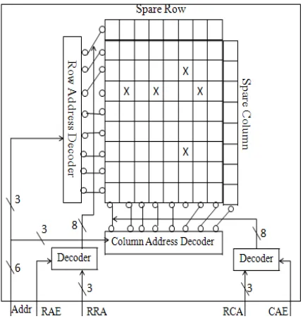
A RAM with redundancies, address decoder and repair register is called a repairable RAM. Figure 2 depicts an example of an 8*8 bit-oriented RAM with 1 spare row and column. Address decoder is used to select the column and row where our desired data lies. Sense amplifier assists the charging of the lines so that the memory cell doesn’t discharge and lose its data. Row repair address and column repair address are the address of the defective row and column respectively. When RAE is high, the RRA is decoded using decoder into control signal to replace the faulty row. Similarly when the CAE is high, the CRA used to repair the faulty column.
B. BIST Circuit:
the BIST circuit, then the faulty information is sent to BIRA circuit.
C. BIRA Circuit:
If BIST detects a fault, then the faulty information is exported to the BIRA circuitry and then BIRA allocates redundancies according to the faulty information provided by the BIST circuit using the redundancy analysis algorithm.
Figure 1. Architecture of BISR Scheme for RAMs
Figure 2. An 8*8 bit oriented Repairable RAM The overall RAM BISR flow as depicted in Figure 1.is described as follows. Firstly, the BIST tests the repairable RAM. If BIST detects a fault, then the fault information is exported to the BIRA circuit. Then, the BIRA circuit collects the faulty information provided by the BIST circuit and allocates redundancies to replace defective elements. When the
repair process finished, the repair signatures are loaded into the repair register in the repairable RAM.
III. MEMORYBIST
MBIST is used to test the on chip memories. The block diagram of the proposed MBIST is shown in figure 3.TPG is used to generate the test sequences which are applied to RAM during testing. Comparator is used to compare the output responses with the expected responses and decision is made whether the RAM is faulty or fault free. A controller is a hardware realization of a memory test algorithm, usually in the form of an FSM. The memory test algorithm here is Marching1/0 algorithm.
Figure 3. Typical block diagram of proposed MBIST This algorithm involves successive writing and reading of 0’s and 1’s into the RAM. The fault location details like fault present, fault row and fault column addresses are given at the output pins. The input pin start is made one when the BIST starts the testing process. The output pin done and progress are resulted to one and zero respectively, after the MBIST process is completed, so that the ReBIRA circuit can start analysis. . The MBSIT FSM is shown in figure 4.
A. State: Idle:
When the input pin start is asserted to zero, the MBIST process is not yet started so it remains in the idle state. Else, the MBIST process enters into the next.
B. State: W1:
C. State: R1:
In this state, when mem_rd is 1, all the memory locations are read through mem_rd_data until row address is equal to zero. When row address is equal to zero, the MBIST process enters into next state.
D. State: W0:
In this state, when mem_wr is 1, all the memory locations are filled with 0’s using mem_wr_data until row address is equal to zero. When row address is equal to zero, the MBIST process into next state.
E. State: R0:
In this state, when mem_rd is 1, all the memory locations are read through mem_rd_data until row address is equal to zero. When row address is equal to zero, the MBIST process into next state called done.
F. State: Done:
At this stage, the MBIST circuit completes the testing of the memory and it again enters into the idle state.
Figure 4. MBIST FSM
IV. PROPOSEDMEMORYREBIRA
If separate BIRA circuit is used for repairing individual RAM in an SOC, then the total area in the SOC is large, since there are many RAMs in a SOC. In the proposed BISR scheme
single BIRA circuit is used for repairing many RAMs. Hence the area cost is reduced.
A. Architecture of ReBIRA:
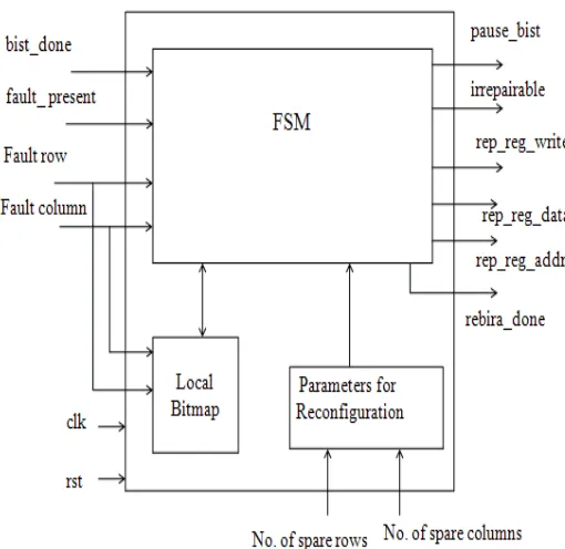
Figure 5 shows the simplified block diagram of ReBIRA used for repairing multiple RAMs in an SOC. If the BIST detects a fault, then the fault information is exported to the ReBIRA circuitry, and then the ReBIRA performs redundancy allocation based on the redundancy algorithm. The redundancy algorithm used here is Fault Checking Algorithm. Fault information includes fault row and fault column Units addresses and the fault_present.
The proposed scheme uses a local bitmap (fault_table) of size 4*64 to store fault information detected by the BIST circuit. Once the local bitmap is full, the MBIST is paused and the ReBIRA allocates redundancies according to the fault information. After, the ReBIRA allocates a redundancy to repair a corresponding faulty row/column, the local bitmap is updated and the MBIST is resumed. This process continues until the test and repair process is completed.
The repair information i.e. repair_register_write, repair_register_data, repair_register_address is sent to the repair register in the repairable RAM once one spare element is allocated. Figure 6 shows the simplified block diagram of repairable RAM. After the ReBIRA circuit allocates redundancies, the repair signatures rep_reg_wr, rep_reg_data and rep_reg_addr are sent to the repair registers present in the repairable RAM. Then, the RAM is repaired using this information as follows.
rep_reg_addr is less than the number of sum of spare rows and spare columns, the rep_reg_data is written into the column_repair_address_reg.
B. Redundancy Analysis Algorithm :
In this section the proposed redundancy algorithm known as Fault-checking algorithm is described. The Fault-Checking algorithm can be used for RAM with different redundancy organization.Fig.6 shows RAM with local spare column and global spare row. In order to carry out the redundancy analysis a local bitmap of size 4X64 is used which is shown in figure 7. The local bitmap is updated with the faulty information detected by BIST circuit. Once the local bit map is full, the Fault-Checking algorithm does the analysis based on the faulty information present in the local bitmap.
Figure 6. RAM with one global spare row and two local spare column
Figure 7. Example of local bitmap
A row address register is used for each row in order to store the faulty row address. Here 64 columns are used. Since there are 64 columns in the memory and 64 columns in the local bitmap, there is a one to one mapping between memory and local bitmap. If the number of rows with faults (NRF) is more than the number of columns with faults (NCF), then a defective column with maximum number of faults (CMF) is replaced with a spare column. If the number of columns with faults (NCF) is more than the number of rows with faults (NRF), then a defective row with maximum number of faults (RMF) is replaced with a spare row. This process continues till all the faults in the local bitmap are repaired.
a. A Fault-Checking Algorithm for allocating spare elements:
a) Start BIST; stop and go to Step 2 when fault is detected.
b) If the fault is repaired jump to step1, else go to Step 3. c) If the local bitmap is full, go to the next step, else, go
to Step 1.
d) If number of faulty rows is greater than the number of faulty column, replace the maximum faulty column with a spare column. Similarly if number of faulty columns is greater than the number of faulty rows, replace the maximum faulty row with a spare row. e) Check if the BIST is completed. If so, go to step 6.
Otherwise, go to Step 1 when the local bitmap is not full; go to Step 4 when the local bitmap is full.
f) If the local bitmap is empty export the repaired addresses and then stop. Otherwise, go to Step 4. C. Design of ReBISR scheme:
Figure 8 shows simplified block diagram of the proposed ReBISR scheme.RAM details table is used for storing the configurations of RAMs which includes the memory data width and depth, number of spare rows and number of spare columns. FSM is the main block that acts as a BIST controller for generating the control signals during testing and repairing. The BIST controller controls the BIST and ReBIRA circuit.
Figure 8. Simplified block diagram of proposed ReBISR for multiple RAMs
is full, the BIST and ReBIRA circuits start the testing and repairing process of RAMs one after other. If the BIST circuit detects a fault, then the fault information is exported to the ReBIRA circuitry, and then the ReBIRA performs redundancy allocation. After the ReBIRA allocates a redundancy to repair a corresponding faulty row or column, the local bitmap is updated and the BIST is resumed. This process continues until the test and repair process is finished. The repair signatures from the ReBIRA circuit are then sent to the repair registers present in the repairable RAMs.
The BIST tests the RAMs once again (after the testing and repairing processes) to ensure that there are no faults present. Figure 9 shows the ReBISR FSM.
Figure 9. ReBISR FSM
V. EXPERIMENTALRESULTS
Table 1 shows four RAMs with various sizes and different redundancy configurations, where (Row X Column) denotes the row address width and column address width; (r, c) denotes the numbers of spare rows and spare columns. Therefore, design parameters of the ReBIRA for these four RAMs as shown in Table I are (Row X Column) = (256 X 64) and (r,c) = (3,3).The proposed ReBISR scheme tests and repairs each RAM serially.
Four RAMs with different number of redundancy configurations are simulated using ModelSim and synthesized using Xilinx tool.
The ReBISR and Dedicated BISR schemes have been synthesized and found the area cost and time cost. Programming is done using Verilog. Table 2 summarizes
simulation and comparison results of the ReBISR scheme and the dedicated BISR (DeBISR) scheme.
Figure 10. Output waveform of ReBIRA
Fig.10 shows the output waveform of ReBIRA module. The ReBIRA waveform shows bit 1 as fault information and bit 0 as fault free information. Address of the faulty row and faulty column are also shown.
Figure 11. Output waveform of MBIST
Figure.11 shows output waveform of MBIST module. If the BIST circuit detects a fault, the corresponding bit of fault_present is made high and the fault information i.e. address is exported to the ReBIRA circuit and the BIST is paused simultaneously.
Table 1. Example of four RAMs with different configurations
RAM No. RAM Size
(Row X Column)
Redundancies (r,c)
RAM0 16X32 (2,2)
RAM1 32X64 (2,3)
RAM2 128X64 (3,2)
Table 2. Simulation and comparison results of the ReBISR scheme and Dedicated BISR scheme
BIRA Scheme RAM Type BIRA Architecture No. of slices used Available slices
Area Cost Clock Cycles % of Area Used
DeBISR WOM Dedicated 7068 8672 High 2,06,700 81%
ReBISR WOM Shared 2865 8672 Low 3,53,200 33%
VI. CONCLUSION
A reconfigurable BISR scheme for repairing multiple repairable RAMs with different sizes and different numbers of redundancies has been presented. An efficient BIRA algorithm for 2-D redundancy allocation has also been introduced. A Comparison of Reconfigurable BISR scheme and Dedicated BISR scheme is done. Experimental results show that the ReBISR scheme incurs low area cost which is only about 33% for four RAMs when compared to 81% for Dedicated BISR for four RAMs which is three times more than ReBISR scheme.
Also, the reconfigurable BISR scheme has greater flexibility than the dedicated BISR scheme as the former one supports the repair of multiple memories. Therefore, the proposed ReBISR scheme has low area cost compared with the other BISR scheme for general applications.
VII.REFERNCES
[1] S. Nakahara, K. Higeta, M. Kohno, T. Kawamura, and K. Kakitani,“Built-in self-test for GHz embedded SRAMs using flexible pattern generator and new repair algorithm,” in Proc. Int. Test Conf. (ITC),1999, pp. 301–310.
[2] Jin-Fu Li, Ruey-Shing Tzeng and Cheng-Wen Wu, “Diagnostic Data Compression Techniques for Embedded
Memories with Built-In Self-Test,” Journal of Electronic Testing: Theory and Applications 18, 515–527, 2002. [3] Y. Zorian, “Embedded memory test&repair: Infrastructure IP
for SOC yield,” in Proc. Int. Test Conf. (ITC), Baltimore, MD, Oct. 2002, pp.340–349.
[4] V. Schober, S. Paul, and O. Picot, “Memory built-in self-repair using redundant words,” in Proc. Int. Test Conf. (ITC), Baltimore, MD, Oct. 2001, pp. 995–1001.
[5] C.-D. Huang, J.-F. Li, and T.-W. Tseng, “ProTaR: An infrastructure IP for repairing RAMs in SOCs,” IEEE Trans. Very Large Scale Integr.(VLSI) Syst., vol. 15, no. 10, pp. 1135–1143, Oct. 2007.
[6] R. Rajsuman, “Design and test of large embedded memories: An overview,” IEEE Des. Test Comput., vol. 18, no. 3, pp. 16–27, May 2001.
[7] T.-W. Tseng and J.-F. Li, “A shared parallel built-in self-repair scheme for random access memories in SOCs,” in Proc. Int. Test Conf. (ITC), Santa Clara, CA, Oct. 2008, pp. 1–9, Paper 25.2.