An Efficient Error Tolerant Adder Using Gate Diffusion Technique
with Low power-high Speed
M. Swathi & C. Kumara Narayana Swamy
1M.Tech Scholar, Department of ECE, Ananthalakshmi Institute of Science & Technology , Ananthapuram , AP,
India.
2Assistant Professor, Department of ECE, Ananthalakshmi Institute of Science & Technology , Ananthapuram , AP,
India.
ABSTRACT-In digital VLSI circuits, perfectly
accurate outputs are not always needed. So designers
have started to design error tolerance circuits which
provide good enough output for computation. On the
basis of this fact, error tolerant adder (ETA) is
designed which provides a way to achieve good
power and speed performance. In this paper, an
emerging logic style of circuit design, gate diffusion
input (GDI) technique is adopted to design a 32-bit
ETA. The proposed design reduces area in terms of
area the transistor count to a great extent as well as
improves the delay and power performance.
Simulation results have shown that proposed design
achieves 38% improvement in the Power when
compared to the existing design.
1.INTRODUCTION
Growing market of multimedia applications
has boosted the need of low power portable devices.
At the same time, high speed performance is also
desirable. To achieve both of these goals
simultaneously, designers have started to
compromise with accuracy because perfectly accurate
results are rarely needed and good enough outputs are
sufficient for computation. This fact has led the
mainly in adders, known as Error Tolerant Adder
(ETA). ETA has been designed to eliminate the need
of carry propagation in addition operation because
carry propagation from one stage to another
consumes a lot of time which causes the slow
operating speed of normal adders. By adopting this
new concept, improvement in speed and power
consumption has been achieved.
In the previous works, either the basic
structure of ETA is altered or the logic style for
hardware implementation is changed. However, the
delay and power performance are improved in these
architectures but the industry demand of low power,
faster adder is still increasing. So there is still a need
of new ETA architecture that deals with these
demands.
In this paper, we will discuss a new logic
style based ETA which is more efficient than the
already existing architectures. This proposed ETA is
designed using GDI logic style which substantially
reduces area in terms of the transistor count. Also the
delay and power performance is also improved in this
new design.
2.LITERATURE REVIEW 2.1 Related Work
The main contribution of this paper presents
the design of modified primitive cells and five
different topologies for full adders at circuit level
implemented based on the GDI technique. The
modified GDI primitive cells are constructed and its
significant variation between CMOS and
conventional GDI are compared. Though GDI
technique offers low power, less transistor count and
fabrication process. The GDI technique requires
twin-well CMOS or Silicon on Insulator (SOI)
process to realize a chip which increases the
complexity as well as the cost of fabrication.
Fig 2.1 Symbol of GDI Cell
Table 1: Logic Faction Implementation with GDI Technique
The different methods are compared with respect to
the layout area, number of devices, delay, and power
dissipation. Issues like technology compatibility,
top-down design, and precomputing synthesis are
discussed, showing advantages and drawbacks of
GDI compared to other methods. Several logic
circuits have been implemented
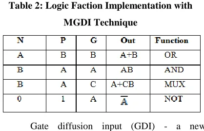
Table 2: Logic Faction Implementation with MGDI Technique
Gate diffusion input (GDI) - a new
technique of low-power digital combinatorial circuit
design - is described. This technique allows reducing
power consumption, propagation delay, and area of
digital circuits while maintaining low complexity of
logic design. Performance comparison with
traditional CMOS and various pass-transistor logic
design techniques is presented. The different methods
are compared with respect to the layout area, number
of devices, delay, and power dissipation. Issues like
technology compatibility, top-down design, and
precomputing synthesis are discussed, showing
advantages and drawbacks of GDI compared to other
methods. Several logic circuits have been
implemented in various design styles. Their
properties are discussed, simulation results are
reported, and measurements of a test chip are
presented.
The GDI approach allows implementation of
a wide range of complex logic functions using only
two transistors. This method is suitable for design of
fast, low power circuits, reduced number of
transistors while allowing simple top- down design.
Gate-Diffusion-Input (GDI) design technique is an
efficient alternative for the logic design in standard
CMOS and SOI technologies. A basic GDI cell
contains four terminals – G node (the common gate
(the outer diffusion node of the PMOS transistor), N
node (the outer diffusion node of the NMOS
transistor), and D node (the common diffusion of
both transistors). P, N and D may be used as either
input or output nodes, depending on the circuit
structure shown in Fig.1 Bulks of both NMOS and
PMOS are connected to N or P (respectively), so it
can be arbitrarily biased in contrast with CMOS
inverter. It must be remarked, that not all the
functions are possible in standard p-well CMOS
process, but can be successfully implemented in
twin-well CMOS or SO1 technologies.
Multiple-input gates can be implemented by combining several
GDI cells.
Modified Gate Diffusion Input
In the basic structure of GDI cell the N
diffusion node and P diffusion node act as a source
and sink. Thereby there in no direct impedance path
between VDD and GND as in the case of CMOS
logic. Therefore this structure will considerably
reduce the effect of dynamic short circuit power
dissipation. The other advantage of this scheme, it
requires lesser area to realize the logic functionality.
While considering the basic structure of AND and
OR gate of GDI the P diffusion (AND gate) is
connected to GND and the N diffusion (OR gate) is
connected to VDD (In Table 1). This type of logic
structure produces a slight degradation at the output
voltage. To obtain the full swing voltage the
proposed primitive cells has a modification in
existing GDI technique. In the proposed cells of
AND gate the P diffusion and Gate terminal are
connected to „A‟ input. Similarly for OR gate the N diffusion and gate terminal are connected to „B‟
input. This modification produces less power
consumption and high VOH, while apparently
maintaining the same reduced transistor count. Fig 3
shows the construction of modified basic gates of
AND, OR, NAND, NOR, XOR, XNOR and MUX.
The modified GDI primitive logic function (MGDI)
is shown in Table.
Fig 2.1: Schematic of SERF Full Adder
3.EXISTING APPROACH
Adders are one of the most essential
components in digital building blocks, however, the
performance of adders become more critical as the
technology advances. The problem of addition
involves algorithms in Boolean algebra and their
respective circuit implementation. Algorithmically,
there are linear-delay adders like ripple-carry adders
(RCA), which are the most straightforward but
slowest. Adders like carry-skip adders (CSKA),
carry-select adders (CSLA) and carry-increment
adders (CINA) are linear-based adders with
optimized carry-chain and improve upon the linear
chain within a ripple-carry adder. Carry-lookahead
adders (CLA) have logarithmic delay and currently
have evolved to parallel-prefix structures. Other
schemes, like Ling adders, NAND/NOR adders and
carry-save adders can help improve performance as
This chapter gives background information
on architectures of adder algorithms. In the following
sections, the adders are characterized with linear gate
model, which is a rough estimation of the complexity
of real implementation. Although this evaluation
method can be misleading for VLSI implementers,
such type of estimation can provide sufficient insight
to understand the design trade-offs for adder
algorithms.
4.IMPLEMENTED APPROACH
The demand for low power adder cores has
been on the rise during years. These units are
essential building blocks of microprocessors and
digital signal processor data paths since hardware
implementation of addition involves the realization
of multitude of distinct data processing subunits that
endure a series of power consuming traditions during
the course of their operations, the power
consumption of adders are in general quite
significant in comparison to that of their integer
counterparts, owing to the presence of a relatively
high traffic of additions in microprocessors and
digital signal processors, the power/performance
implications of adders directly impact the
power/performance desirability of the target
applications. Addition is believed to be the most
frequent computer arithmetic operation, also the
other operations such as the subtraction,
multiplication and division can be derived from
addition and hence adders are often seen as the most
significant part of arithmetic unit.
Increase in demand for the high fidelity
portable devices has laid emphasis on the
development of low power and high performance
systems. In the next generation processors, the low
power design has to be incorporated in to
fundamental computation units, such as adders. The
characterization and optimization of such low power
adder will aid in comparison and choice of adder
modules in system design.
The need for low-power VLSI system arises
from two main forces. First, with the steady growth
of operating frequency and processing capacity per
chip, larger currents have to be delivered and the
heat due to larger power consumption must be
removed by proper cooling technique. Second,
battery life in portable electronic devices is limited.
Low power design directly leads to prolonged
operation time in these portable devices.
Addition is a fundamental operation in most
signal processing algorithms. Adders have a larger
area, long latency and consume considerable power.
Therefore low power adder design has been an
important part in low-power VLSI system design.
There has been extensive work on low power adders
at technology, physical, circuit and logic levels. A
systems performance is generally determined by the
performance of adder because the adder is generally
the slowest element in the system. Furthermore, it is
generally the most area consuming. Hence,
optimizing the speed and area of the adders is a
major design issue. However, area and speed are
usually conflicting constraints so that improving
speed results mostly in larger areas. As a result, a
whole spectrum of adders with different area, speed
constraints has been designed with fully parallel.
Existing conventional adders are no longer suitable
for larger adders because of its low-speed speed
performance.
5.Design Of Accurate And Inaccurate Part Ripple carry adder is used for addition logic
the next stage. In a ripple carry adder the sum and
carryout bits of any half adder stage is not valid until
the carry in of the stage occurs. The propagation
delay inside the logic circuitry is the reasons behind
this, propagation delay is the time elapsed between
the application of an input and occurrence of the
corresponding output. The construction of 4 bit
ripple carry adder using PG logic is shown in figure.
Each block of the ripple carry adder is designed
using the 28 transistor the construction is depleted. A
ripple carry adder is a logic circuit in which the
carry-out of each full adder is the carry in of the
succeeding next most significant full adder. It is
called a ripple carry adder because each carry bit
gets rippled into the next stage. In a ripple carry
adder the sum and carry out bits of any half adder
stage is not valid until the carry in of that stage
occurs.Propagation delays inside the logic circuitry
is the reason behind this. Propagation delay is time
elapsed between the application of an input and
occurance of the corresponding output. Consider a
NOT gate, When the input is “0” the output will be
“1” and vice versa. The time taken for the NOT
gate’s output to become “0” after the application of logic “1” to the NOT gate’s input is the propagation
delay here. Similarly the carry propagation delay is
the time elapsed between the application of the carry
in signal and the occurance of the carry out (Cout)
signal.
Fig 5.1: Ripple Carry Adder
Carry generation(G) and carry
propagation(P) signals in ripple carry adders are used
to describe whether a group of spanning bits i…..j
inclusive, generate a carry or propagate carry as the
P and G signals will have already stabilized by the
time the carry arrives. The critical path of the carry
ripple adder passes from carry in to carry out along
the chain majority gates.
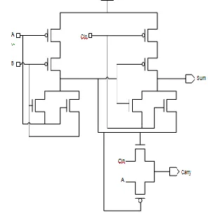
Fig 5.2:28 transistor full adder
The critical path delay of the ripple carry adder can
be calculated by tripple = tpg+(N-1) tAO + txor
The working principle of the inaccurate part
consists of control logic. The control logic enables
the OR operation if its value is zero or else disables
output to go a logic high. The construction of the
control logic is shown in the figure. The aspect ratio
of the PMOS transistor M3 should be varied to attain
a proper high state.
Fig 5.3: Control Logic
The individual addition of the inaccurate
part is fed to the control logic. This CTL input
controls the output of the carry free addition block of
the inaccurate part. When both the bits or either of
the bits are low, then CTL remains low and CTL is
set to logic high when both the bits goes high there
by making the output high for any input that comes
after the bits that produced high. The truth table of
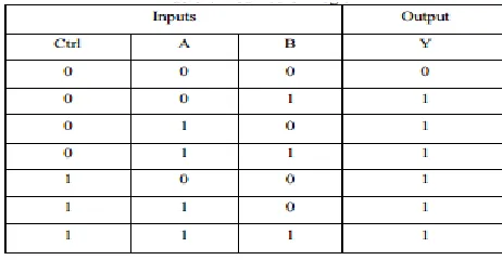
the modified OR logic is shown in table.
Table 5.1: Modified OR Logic
6. GDI Based Eta Architecture
6.1 Background of GDI Technique
The above mentioned architecture of ETA has
been implemented using the conventional CMOS
logic style. In our proposed architecture, gate
diffusion input (GDI) method, is used for hardware
implementation. GDI logic style has emerged as a
new logic design style in which the transistor count
decreases drastically. By using this method the basic
logic functions can be designed using only two
transistors which require four, six or even twelve
transistor in conventional CMOS logic style. A
simple GDI cell is shown in figure. It is a three input
cell where the three inputs are: G (common gate
input to both PMOS and NMOS), P (input to
source/drain of PMOS) and N (input to source/drain
of NMOS). Different input combinations are applied
to these input pins to obtain various logic functions
with lesser number of transistors. Table shows that a
number of Boolean functions can be implemented by
some simple changes in input configuration using the
GDI cell of Fig.
Table 6.1: Various Logic Functions
Implementation Using GDI Method
6.2 Power Reduction in GDI Technique
Besides reducing the transistor count, GDI
method also improves the power performance of
NMOS can be given as:
where W is the transistor’s width, L is the transistor’s length, VT is the thermal voltage,
Vds is the drain-source voltage, VgSis the
gate-source voltage, K' and m are process constants,
and Vthis the threshold voltage.
It can be noticed here that in CMOS logic
circuits the pull-up and pull-down networks are
always connected to VDD and ground respectively
which is not in the case of GDI cell. So a
sub-threshold leakage current is always present in
CMOS logic circuits whereas in GDI cell, it is
absent in almost half of the possible cases. Hence a
substantial reduction in power is achieved in GDI
cell based designs.
6.3 Proposed Architecture
In our proposed architecture, the accurate
and inaccurate parts of ETA are implemented using
the GDI cell of Fig. In proposed accurate part, the
adder cells are designed using GDI logic style. Fig
shows the existing and proposed architecture of the
adder cells for accurate part. A single adder cell
requires 28 transistors when implemented using
CMOS logic style whereas it requires only 12
transistors when implemented using GDI technique.
It is worth to note here that the delay in ETA is only
due the carry propagation in accurate part because
no carry propagation occurs in inaccurate part. So
as the transistor count is decreased in accurate part,
it will improve the overall delay of ETA.
Fig (a): Schematic Diagram of Adder Cell Using
CMOS Logic Style
In similar manner, the MXOR cell in carry free
addition block also implemented block using GDI
method for out proposed architecture. Figure 6 shows
existing and proposed method of MXOR cell .It is
clear from the schematic diagram that transistor count
drastically reduced in both the full adder and MXOR
cell.
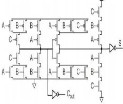
Fig (b): Schematic Diagram of MXOR Cell
Fig (c): Schematic Diagram of MXOR Cell
Using GDI Logic Style
SIMULATION & RESULTS 7.1 Simulation
Along with the proposed CAM design, both
NOR- and NAND-type ML CAMs of size 4 × 3 were
implemented in the 65-nm technology node and post
layout simulation was performed to measure their
performance using DSCH and Microwind. Following
figures shows the DSCH and Microwind simulation
result and the layout of the proposed CAM cell.
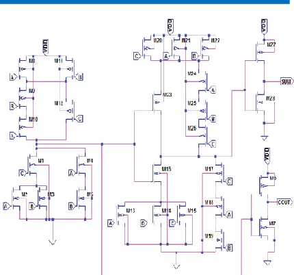
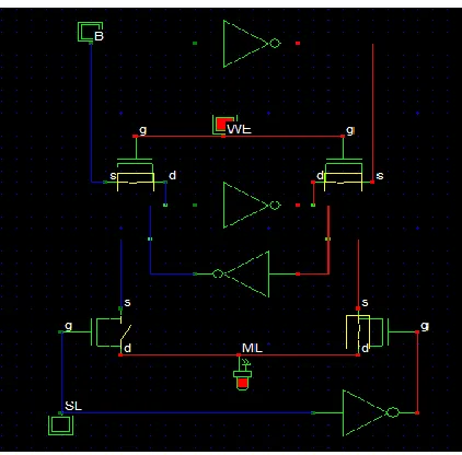
Fig 7.1(a): Schematic of 8T CAM cell
Fig 7.1(b): Timing Diagram of 8T CAM cell
Fig 7.1(d): Simulation of Layout of 8T CAM cell
Fig 7.1(e): Schematic of Proposed 4x3 CAM array
7.2 Results
Fig 7.2(a): Timing Diagram of Proposed 4x3 CAM array
Fig 7.2(b): Layout of Proposed 4x3 CAM array
Fig 7.2(c): Simulation of Layout of Proposed 4x3 CAM array
RESULTS AND COMPARISON
To illustrate the merits of our proposed GDI
based ETA, we simulated it along with the exiting
CMOS logic based ETA. Both adders are
are drawn in LTspice software. To construct the
models of both architectures, HSPICE software is
used. 20 sets of input operands are created
randomly. Each input set is simulated for both
adders and power consumption is recorded. With
20 sets of results, average power was computed. The
worst case input was applied to simulate the worst
case delay. The worst case input refers to the case
when all the input bits of both operands are high. In
this case carry will ripple through all the adder cells
of accurate part hence resulting in worst case delay.
Transistor count was directly obtained from the
HSPICE software. A comparative analysis of both
designs is shown in Table.
Table :Comparative Analysis of ETA Design
Parameters Conventional
ETA
GDI Based ETA Transistor Count
(N) 1036 54
4
Delay(ns) 0.
50
0. 3 9
Power (μW) 4.
36
3. 5 1
PDP (pJ) 2.
21
1. 3 8 Simulation results shows that proposed
architecture requires 48% less transistor count
and attains 38% improvement in power-delay
product (PDP). This reduction in transistor count in
our proposed architecture is justified in Table.
Table: Justification of Reduced Transistor Count
CONCLUSION
In this paper, a new architecture of ETA is proposed
based on GDI logic style. This proposed architecture
is implemented and compared with the existing
conventional ETA. This new design has
outperformed the previous one in terms of power
dissipation, speed and transistor count. This proposed
architecture can be used in the application where
speed, area and power are of greater concern than
accuracy.
FUTURE SCOPE
However, there is a problem of reduced
voltage swing in this new design. So to improve the
voltage swing, further work can be done in this
direction.
REFERENCES
[1] Ning Zhu, Wang Ling Goh, Weija Zhang,
KiatSeng Yeo, and ZhiHui Kong, “Design of
Low-Power High-Speed
Truncation-Error-Tolerant Adder and Its Application in Digital
Signal Processing”, IEEE Transactions On
Very Large Scale Integration (VLSI) Systems,
[2] Anand N George Joseph, Suwin Sam Oommen
and K Sivasankaran, ”ASIC Implementation of a High Speed Error Tolerant Adder”,
International Conference on Electronics and
Communication Systems (ICECS), February
2014, pg. 1-4.
[3] S.Sathish Kumar, V.Muralidharan and S.Raja,
”Power and Area Efficient Error Tolerant
Adder Using Pass Transistor XOR Logic in
VLSI Circuits”, International Journal of
Advanced Research in Computer Engineering
& Technology (IJARCET), Vol. Issue 3,
March2014.
[4] Srisainadh.I and Srinath.B, “Design of Low Power High Speed VLSI Error-Tolerant Adder”
International Journal of Research and
Innovative Technology, Vol. 1, Issue 1,
April2014.
[5] Ning Zhu, Wang Ling Goh, and KiatSeng Yeo
“An Enhanced Low- Power High-Speed
Adder For Error-Tolerant
Application”,International Symposium on
Integrated circuits(ISIC), December 2009, pg.
69-72.
[6] Melvin A. Breuer and Haiyang Zhu,
“Error-tolerance and multi- media,”in Proc. of the
2006 International Conference on Intelligent
Information Hiding and Multimedia Signal
Processing, 2006.
[7] K. J. Lee, T. Y. Hsieh and M. A. Breuer, “A
novel testing methodology based on error-rate
to support error-tolerance,” in Proc. of
International Test Conference, pp. 1136–1144,
2005.
[8] I. S. Chong and A. Ortega, “Hardware testing
for error tolerant multimedia compression
based on linear transforms,” Defect and Fault
Tolerance in VLSI Systems Symp., 2005.
[9] A. Morgenshtein and A. Fish, I. A. Wagner,
“Gate-Diffusion Input (GDI) – A
power-efficient method for digital combinatorial
circuits, IEEE Transactions on VLSIsystems,
vol.10, no. 5, October, 2001.
[10] Atul Kumar Nishad, RajeevanChandel,
”Analysis of Low Power High Performance
XOR Gate using GDI Technique”,
International Conference on Computational
Intelligence and Communication Systems,