University of South Carolina
Scholar Commons
Theses and Dissertations
2016
Applications Of Impedance Identification To
Electric Ship System Control And Power
Hardware-In-The-Loop Simulation
Jonathan SiegersUniversity of South Carolina
Follow this and additional works at:https://scholarcommons.sc.edu/etd Part of theElectrical and Electronics Commons
This Open Access Dissertation is brought to you by Scholar Commons. It has been accepted for inclusion in Theses and Dissertations by an authorized administrator of Scholar Commons. For more information, please [email protected].
Recommended Citation
Siegers, J.(2016).Applications Of Impedance Identification To Electric Ship System Control And Power Hardware-In-The-Loop Simulation.
APPLICATIONS OF IMPEDANCE IDENTIFICATION TO ELECTRIC SHIP SYSTEM
CONTROL AND POWER HARDWARE-IN-THE-LOOP SIMULATION
by
Jonathan Siegers
Bachelor of Science
University of South Carolina, 2011
Submitted in Partial Fulfillment of the Requirements
For the Degree of Doctor of Philosophy in
Electrical Engineering
College of Engineering and Computing
University of South Carolina
2016
Accepted by:
Enrico Santi, Major Professor
Herbert Ginn, Committee Member
Andrea Benigni, Committee Member
Jason Bakos, Committee Member
DEDICATION
ACKNOWLEDGEMENTS
My greatest appreciation goes to my Academic Advisor and mentor, Dr. Enrico
Santi. His enthusiasm and encouragement over the course of my doctoral program have
inspired me to always seek a deeper and more complete understanding of concepts. My
skills as a researcher and approach to engineering are a product of his expert guidance
and I am sincerely grateful to have had the opportunity to broaden my theoretical and
practical knowledge through his teaching.
I would also like to express my gratitude to my Committee Members, Dr. Herbert
Ginn, Dr. Andrea Benigni, and Dr. Jason Bakos for their valuable feedback in the
preparation of this dissertation. Their time and effort has helped ensure meaningful,
quality research. My special thanks also goes out to Dr. Tangali Sudarshan and Dr.
Krishna Mandal for providing me with early research experiences and for encouraging
me to pursue a Ph.D.
I have benefitted greatly from the support of the administrative staff of the
Electrical Engineering Department. I am particularly thankful for the Power Electronics
Group Program Coordinator Hope Johnson, Assistant to the Chair Nat Paterson, Graduate
Coordinator Ashley Burt, and Computer Support Manager David London. My sincere
appreciation also goes to David Metts for his friendship and support throughout my
There are many former and current members of the Electrical Engineering
Graduate program to whom I am greatly indebted. I would like to express my thanks to
Dr. Antonino Riccobono, Dr. Pietro Cairoli, Dr. Daniel Martin, Dr. Isaac Nam, Dr. Ozan
Gulbudak, and Dr. Kang Peng for their personal and technical guidance throughout my
graduate studies. My appreciation also goes to the current Power Electronics Group for
their strong collaborative research spirit and enthusiasm. In particular, I am grateful for
the invaluable assistance of Silvia Arrúa in the development of the analytic converter
system models and for assisting me in the laboratory during the hardware setup and
experimental data collection contained in this dissertation.
I would like to acknowledge the support of the Office of Naval Research and
Electric Ship Research and Design Consortium (ESRDC) who provided the motivation
and funding for this research under grant N00014-14-1-00165 and N00014-08-1-0080.
Finally, I want to express my thanks for the unending support and love of my
family. My parents have instilled in me a work ethic and determination that has allowed
me to achieve far more than I could have imagined. I thank my sister, Dr. Justine Petty,
for serving as a positive role model to me and for the healthy academic competition I
ABSTRACT
Recent advances in semiconductor technology, controls, and switching converter
topologies have resulted in the increasing application of power electronics in power
distribution systems. Power electronic enabled distribution systems have inspired a
renewed interest in DC distribution architectures as an appealing alternative to traditional
AC methods due to the significant performance and efficiency gains they offer. However,
the notional power electronic based DC distribution system is a complex and extensively
interconnected system consisting of multiple power converters. As a result, a number of
system-level challenges related to stability arise due to interaction among multiple power
converters. In addition, the power distribution system is likely to undergo configuration
variations as the system is subject to component upgrades, changes in power sources and
loading, and even contingency scenarios involving fault conditions. The design of this
type of system is difficult due to the general lack of proper analysis tools and limited
understanding of the problem.
To address these design challenges, an approach to control design that accounts
for converter interactions and allows for impedance based control is proposed. The use of
impedance monitoring via wideband impedance identification techniques provides
interesting opportunities for the development of a robust and adaptive control strategy.
system bus impedance, enacting revised control strategies with the intent of stabilizing
the system as its dynamics evolve over time.
Secondly, the use of Power Hardware-in-the-Loop (PHIL) simulation is
investigated for early system testing. As parts of the distribution system become available
in hardware, it is desirable that they be evaluated under realistic system conditions. PHIL
allows for advanced studies to be performed on system interactions by virtually coupling
a real-time software simulation of electrical components to a physical piece of hardware
through the use of an interfacing amplifier and appropriate control algorithm. Use of a
PHIL test platform allows for system interaction studies to be performed early on in
hardware development and provides an enhanced ability to study potential system-level
problems and develop suitable solutions. Wideband impedance identification is utilized
to complement the PHIL simulation, providing additional characterization of the
hardware under test as well as critical information that is used to ensure stability and
TABLE OF CONTENTS
DEDICATION ... iii
ACKNOWLEDGEMENTS ... iv
ABSTRACT ... vi
LIST OF TABLES ... xi
LIST OF FIGURES ... xii
LIST OF SYMBOLS ... xx
LIST OF ABBREVIATIONS ... xxii
CHAPTER1:INTRODUCTION ... 1
1.1 STABILITY AND PERFORMANCE ISSUES IN MULTI-CONVERTER DCSYSTEMS ... 1
1.2 STATE OF THE ART ... 4
1.3 CONTENTS OF DISSERTATION ... 17
CHAPTER2:MULTI-CONVERTER SYSTEM MODELING ... 21
2.1 RESISTIVELY TERMINATED MODELING ... 21
2.2 UNTERMINATED TWO-PORT SMALL-SIGNAL MODELING ... 25
2.3 EXAMPLE MULTI-CONVERTER SYSTEM MODEL AND PARAMETER EXTRACTION .. 31
2.4 SUMMARY OF MULTI-CONVERTER SYSTEM MODELING ... 35
CHAPTER3:MULTI-CONVERTER SYSTEM STABILITY EVALUATION AND IMPROVEMENT 36 3.1 PASSIVITY BASED STABILITY CRITERION FOR MULTI-BUS SYSTEMS ... 36
3.2 ALLOWABLE IMPEDANCE REGION ... 40
3.3 POSITIVE FEED-FORWARD CONTROL AND DAMPING IMPEDANCE DESIGN... 45
3.5 EXAMPLE ANALYTIC SYSTEM EVALUATION AND CONTROL DESIGN ... 54
3.6 CONCLUSION OF CONVERTER SYSTEM STABILITY, EVALUATION, AND ANALYTIC DESIGN... 69
CHAPTER4:SIMULATION AND EXPERIMENTAL RESULTS FOR MULTI-BUS STABILITY AND PERFORMANCE ENHANCEMENTS... 71
4.1 SIMULATION RESULTS ... 72
4.2 EXPERIMENTAL RESULTS ... 82
4.3 CONCLUSION OF SIMULATION AND EXPERIMENTAL RESULTS ... 106
CHAPTER5:POWER HARDWARE-IN-THE-LOOP SIMULATION ... 107
5.1 INTERFACE STABILITY ... 108
5.2 PHILSYSTEM ACCURACY ... 120
5.3 CONCLUSION OF PHILSTABILITY AND ACCURACY IMPROVEMENTS ... 135
CHAPTER6:SIMULATED MVDCPHILSTABILITY EVALUATION AND IMPEDANCE BASED CONTROL DESIGN ... 137
6.1 MVDCSYSTEM DESCRIPTION ... 137
6.2 PHILINTERFACE ALGORITHM ACCURACY AND STABILITY EVALUATION ... 139
6.3 MVDCSYSTEM STABILITY ANALYSIS AND CONTROLLER DESIGN ... 143
6.4 CONCLUSION OF MVDCSYSTEM DESIGN USING PHILSIMULATION ... 147
CHAPTER7:CONCLUSION AND FUTURE WORK ... 149
7.1 CONCLUSIONS ... 149
7.2 FUTURE WORK ... 151
REFERENCES ... 159
APPENDIXA:CROSS-CORRELATION BASED SYSTEM IDENTIFICATION TECHNIQUE ... 163
A.1 CROSS-CORRELATION METHOD ... 163
A.2 IMPROVEMENTS TO CROSS-CORRELATION METHOD ... 164
B.1 OPEN-LOOP UNTERMINATED VSIG-PARAMETERS ... 166
B.2 COMPLETE FOUR-CONVERTER SYSTEM MODEL ... 171
APPENDIXC:ADDITIONAL SUBSYSTEM BLOCK DIAGRAMS ... 174
C.1 FOUR-CONVERTER MULTI-BUS SYSTEM ... 174
C.2 PHILINTERFACE AMPLIFIER ... 177
LIST OF TABLES
Table 3.1. Complete Converter Hardware and Control Parameters ... 55
Table 3.2. Steady-State Operating Point Specifications for Scenario 1 ... 56
Table 3.3. Bus 1 Impedance and PFF Control Design Summary (Scenario 1) ... 61
Table 3.4. Steady-State Operating Point Specifications for Scenario 2 ... 63
Table 3.5. Bus 2 Impedance and PFF Control Design Summary (Scenario 2) ... 66
Table 4.1. Normalized Bus 1 Impedance and Adaptive PFF Control Design Summary (Scenario 1) ... 95
Table 4.2. Normalized Bus 2 Impedance and Adaptive PFF Control Design Summary (Scenario 2) ... 102
Table 5.1. Complete PHIL System Converter Hardware and Control Parameters for PHIL System Stability Evaluation ... 113
Table 5.2. Complete Converter Hardware and Control Parameters for PHIL System Accuracy Evaluation ... 124
Table 5.3. Interface Amplifier Design Parameters ... 128
Table 6.1. Complete PHIL Simulated Converter Parameters ... 138
Table 6.2. Complete PHIL Interface Amplifier Parameters ... 139
LIST OF FIGURES
Figure 1.1. Proposed MVDC power distribution system for the US Navy’s all-electric
ship (simplified). ... 2
Figure 1.2. Conceptual diagram of equivalent interacting source and load subsystem. ... 6
Figure 1.3. Conceptual diagram of source subsystem impedance measurement. ... 10
Figure 1.4. Conceptual diagram of load subsystem impedance measurement. ... 10
Figure 1.5. Example wideband impedance construction as the difference of control-to-voltage and control-to-current converter transfer functions. ... 11
Figure 1.6. General CHIL simulation scheme including real-time software simulator, low-level signal interfacing, and controller device under test. ... 15
Figure 1.7. General PHIL simulation scheme including real-time software simulator, low-level signal interfacing, power interface, and the power device under test. ... 15
Figure 2.1. Idealized model of buck switching converter with ideal voltage source and resistive load. ... 22
Figure 2.2. Model structure of (a) unterminated two-port hybrid g-parameter model and (b) buck switching converter. ... 25
Figure 2.3. Generalized switching converter block diagram operating (a) open-loop, (b) under inductor current mode (CM) control, (c) with feedback output voltage and feed-forward input voltage control (FFFB), and (d) complete closed-loop converter. ... 28
Figure 2.4. Scaled notional multi-bus MVDC distribution system. ... 32
Figure 2.5. Small-signal system model construction. ... 33
Figure 3.1. Conceptual multi-bus power distribution system showing multiple interconnections using power converter interfaces. ... 37
Figure 3.2. (a) Equivalent interacting source and load subsystems and (b) 1-port network. ... 40
Figure 3.4. Comparison of realistic bus impedance Nyquist contour for an Allowable Impedance Region specified by (a) vertical asymptote limit and (b) semicircle centered at the origin. ... 44
Figure 3.5. Nyquist contour of simplified bus impedance under PFF control for varying values of Km (ζmin = 0.5). ... 49
Figure 3.6. Bode plot and Allowable Impedance Region analysis (ζmin = 0.5) on realistic
system bus self-impedance under FB control only. ... 51
Figure 3.7. Adaptive control algorithm for MVDC distribution system combining the PBSC, AIR analysis, and PFF control techniques with online impedance monitoring. ... 53
Figure 3.8. Example timing diagram of adaptive control scheme for impedance based control. ... 54
Figure 3.9. Scaled notional multi-bus MVDC distribution system. ... 55
Figure 3.10. Bode plot of Scenario 1 Bus 1 analytic self-impedance and associated source
and load converter impedances for system operating under
feedback control only. ... 58
Figure 3.11. Bode plot of Scenario 1 Bus 2 analytic self-impedance and associated source and load converter impedances for system operating under FB control only. ... 58
Figure 3.12. Nyquist plot of Scenario 1 normalized analytic bus impedances and
Allowable Impedance Region (ζmin = 0.5) for system operating under FB
control only. ... 60
Figure 3.13. Bode plot of Scenario 1 Bus 1 analytic self-impedance and associated source and load converter impedances for system operating under FFFB control. ... 62
Figure 3.14. Bode plot of Scenario 1 Bus 2 analytic self-impedance and associated source and load converter impedances for system operating under FFFB control. ... 62
Figure 3.15. Nyquist plot of Scenario 1 normalized analytic bus impedances and
Allowable Impedance Region (ζmin = 0.5) for system operating under
FFFB control. ... 63
Figure 3.16. Bode plot of Scenario 2 Bus 1 analytic self-impedance and associated source and load converter impedances for system operating under FB control only. ... 65
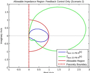
Figure 3.18. Nyquist plot of Scenario 2 normalized analytic bus impedances and
Allowable Impedance Region (ζmin = 0.5) for system operating under FB
control only. ... 67
Figure 3.19. Bode plot of Scenario 2 Bus 1 analytic self-impedance and associated source and load converter impedances for system operating under FFFB control. ... 68
Figure 3.20. Bode plot of Scenario 2 Bus 2 analytic self-impedance and associated source and load converter impedances for system operating under FFFB control. ... 68
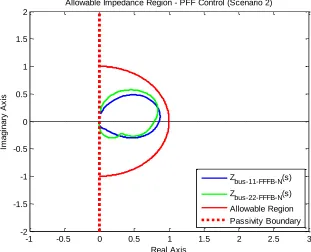
Figure 3.21. Nyquist plot of Scenario 2 normalized analytic bus impedances and
Allowable Impedance Region (ζmin = 0.5) for system operating under FFFB
control. ... 69
Figure 4.1. PLECS diagram of scaled notional multi-bus MVDC distribution system .... 73
Figure 4.2. Bode plot of simulated Scenario 1 bus self-impedance Zbus-11 non-parametric
estimation and analytic model for system operating under FB
and FFFB control. ... 75
Figure 4.3. Bode plot of simulated Scenario 1 bus cross-impedance Zbus-12 non-parametric
estimation and analytic model for system operating under FB
and FFFB control. ... 75
Figure 4.4. Bode plot of simulated Scenario 1 bus cross-impedance Zbus-21 non-parametric
estimation and analytic model for system operating under FB
and FFFB control. ... 76
Figure 4.5. Bode plot of simulated Scenario 1 bus self-impedance Zbus-22 non-parametric
estimation and analytic model for system operating under FB
and FFFB control. ... 76
Figure 4.6. Time domain simulation of Scenario 1 MVDC bus voltages under (blue) FB control only and (red) FFFB control during BKL voltage reference step. ... 77
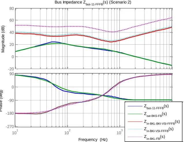
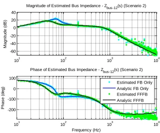
Figure 4.7. Bode plot of simulated Scenario 2 bus self-impedance Zbus-11 non-parametric
estimation and analytic model for system operating under FB
and FFFB control. ... 79
Figure 4.8. Bode plot of simulated Scenario 2 bus self-impedance Zbus-12 non-parametric
estimation and analytic model for system operating under FB
and FFFB control. ... 79
Figure 4.9. Bode plot of simulated Scenario 2 bus self-impedance Zbus-21 non-parametric
estimation and analytic model for system operating under FB
Figure 4.10. Bode plot of simulated Scenario 2 bus self-impedance Zbus-22 non-parametric
estimation and analytic model for system operating under FB
and FFFB control. ... 80
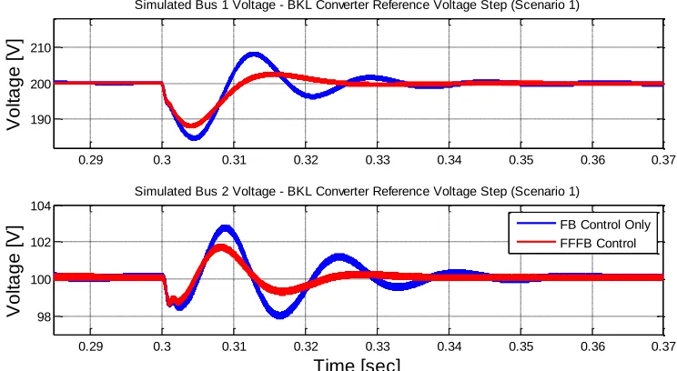
Figure 4.11. Time domain simulation of Scenario 2 MVDC bus voltages under (blue) FB control only and (red) FFFB control during BKL voltage reference step. ... 81
Figure 4.12. Experimental test setup for scaled notional MVDC power distribution system as built in the laboratory. ... 82
Figure 4.13. Experimental PRBS converter hardware showing power module, sensing board connections, and output filter as well as LabView sensing board and I/O for wideband impedance identification. ... 83
Figure 4.14. Wideband impedance identification LabView Virtual Instrument Front Panel showing preliminary voltage and current FFT results and constructed non-parametric impedance. ... 85
Figure 4.15. Control algorithm for load buck converter (BKL) implemented in Simulink using dSPACE block-set. ... 86
Figure 4.16. Control algorithm for voltage source inverter (VSI) implemented in Simulink using dSPACE block-set. ... 86
Figure 4.17. dSPACE ControlDesk layout for load buck converter (BKL). ... 87
Figure 4.18. dSPACE ControlDesk layout for load voltage source inverter (VSI). ... 88
Figure 4.19. Bode plot of experimental Scenario 1 bus self-impedance Zbus-11-FB
non-parametric estimation and logarithmically thinned data for system operating under FB control only. ... 90
Figure 4.20. Bode plot of experimental Scenario 1 bus self-impedance Zbus-11-FB analytic
model, non-parametric estimation and fitted, parametric model for system operating under FB control only. ... 90
Figure 4.21. Bode plot of experimental Scenario 1 bus self-impedance Zbus-22-FB analytic
model, non-parametric estimation and fitted, parametric model for system operating under FB control only. ... 91
Figure 4.22. Bode plot of experimental Scenario 1 bus self-impedance Zbus-11-FFFB analytic
model and non-parametric estimation for system operating under FFFB control. 93
Figure 4.23. Bode plot of experimental Scenario 1 bus self-impedance Zbus-22-FFFB analytic
Figure 4.24. Experimental time domain results of Scenario 1 AC coupled bus voltages under (blue) FB control only and (red) FFFB control during BKL voltage reference step. ... 94
Figure 4.25. Nyquist plot of “black-box” Scenario 1 normalized estimated bus
impedances and AIR (ζmin = 0.5) for system operating under FB control only
(dashed) and FFFB control (solid). ... 95
Figure 4.26. Bode plot of experimental “black-box” Scenario 1 bus self-impedance
Zbus-11-FFFB non-parametric estimation and fitted, parametric model for system
operating under FFFB control. ... 96
Figure 4.27. Bode plot of experimental “black-box” Scenario 1 bus self-impedance
Zbus-22-FFFB non-parametric estimation and fitted, parametric model for system
operating under FFFB control. ... 97
Figure 4.28. Experimental time domain results of “black-box” Scenario 1 AC coupled bus voltages under (blue) FB control only and (red) FFFB control during BKL voltage reference step. ... 97
Figure 4.29. Bode plot of experimental Scenario 2 bus self-impedance Zbus-11-FB analytic
model, non-parametric estimation and fitted, parametric model for system operating under FB control only. ... 98
Figure 4.30. Bode plot of experimental Scenario 2 bus self-impedance Zbus-22-FB analytic
model, non-parametric estimation and fitted, parametric model for system operating under FB control only. ... 99
Figure 4.31. Bode plot of experimental Scenario 2 bus self-impedance Zbus-11-FFFB analytic
model and non-parametric estimation for system operating
under FFFB control. ... 100
Figure 4.32. Bode plot of experimental Scenario 2 bus self-impedance Zbus-22-FFFB analytic
model and non-parametric estimation for system operating
under FFFB control. ... 100
Figure 4.33. Experimental time domain results of Scenario 2 AC coupled bus voltages under (blue) FB control only and (red) FFFB control during BKL voltage reference step. ... 101
Figure 4.34. Nyquist plot of “black-box” Scenario 2 normalized estimated bus
impedances and AIR (ζmin = 0.5) for system operating under FB control only
(dashed) and FFFB control (solid). ... 103
Figure 4.35. Bode plot of experimental “black-box” Scenario 2 bus self-impedance
Zbus-11-FFFB non-parametric estimation and fitted, parametric model for system
Figure 4.36. Bode plot of experimental “black-box” Scenario 2 bus self-impedance
Zbus-22-FFFB non-parametric estimation and fitted, parametric model for system
operating under FFFB control. ... 105
Figure 4.37. Experimental time domain results of “black-box” Scenario 2 AC coupled bus voltages under (blue) FB control only and (red) FFFB control during BKL voltage reference step. ... 105
Figure 5.1. PHIL representation of a multi-converter system showing separation of software simulated components and physical hardware. ... 107
Figure 5.2. Damping Impedance Method (DIM) interface algorithm. ... 109
Figure 5.3. Damping Impedance Method (DIM) interface algorithm block diagram. ... 110
Figure 5.4. Damping Impedance Method (DIM) including wideband impedance identification. ... 112
Figure 5.5. Scaled MVDC distribution system PHIL test scenario comprised of an interconnected source buck converter and load VSI and load buck converter. .. 114
Figure 5.6. Nyquist plot of DIM IA loop gain using resistive estimate of Z* (blue) and
wideband estimate (red) for MVDC system ... 115
Figure 5.7. Simulink diagram of simulated PHIL test platform showing (a) naturally coupled MVDC system and PHIL simulation with HUT connection, and (b) DIM IA and ROS simulation ... 116
Figure 5.8. Overview of bus voltage time-domain simulation showing converter startup and load step change for a reference system (blue) and PHIL system (red). ... 117
Figure 5.9. Zoom of load step change for a reference system (blue) and PHIL experiment (red) showing oscillation in PHIL system. ... 118
Figure 5.10. Bode plot of the HUT impedance non-parametric estimation data (blue), analytic model (red), and (b) fitted parametric model of the HUT impedance (dashed green) for MVDC system. ... 119
Figure 5.11. Zoom of load step change for a reference system (blue) and PHIL experiment (red) showing elimination of interface oscillations. ... 119
Figure 5.12. Comparison of ROS impedance (blue), DIM IA output impedance (red), and interface amplifier output impedance ZAB-HIGH (green). ... 126
Figure 5.14. Simulink diagram of simulated PHIL test platform showing (a) interface
amplifier and HUT interconnection and (b) DIM IA and ROS simulation ... 129
Figure 5.15. Nyquist plot of DIM IA loop gain using resistive estimate (blue) and wideband estimate (red) of Z*. ... 130
Figure 5.16. Bode plot of non-parametric estimate HUT impedance (blue) and parametric model (red). ... 130
Figure 5.17. Transient simulation of HUT startup and ROS startup for PHIL interface using (a) high output impedance interface amplifier ZAB-HIGHand (b) low output impedance interface amplifier ZAB-LOW. ... 133
Figure 5.18. Transient simulation of ROS reference step and HUT reference step for PHIL interface using (a) high output impedance interface amplifier ZAB-HIGH and (b) low output impedance interface amplifier ZAB-LOW... 135
Figure 6.1. Scaled MVDC distribution system PHIL test scenario comprised of an interconnected source buck converter, load buck converter, and load VSI. ... 138
Figure 6.2. Comparison of ROS impedance (blue), DIM IA output impedance (red), and interface amplifier output impedance (green). ... 141
Figure 6.3. Nyquist plot of DIM IA loop gain using resistive estimated (blue) and wideband estimate (red) of Z*. ... 142
Figure 6.4. Bode plot of non-parametric estimated HUT impedance (blue) and parametric model (red). ... 143
Figure 6.5. Bode plot of non-parametric estimated bus impedance (blue) and fitted parametric model (red) of PHIL simulated system. ... 144
Figure 6.6. Nyquist plot of normalized estimated PHIL simulated bus impedance and AIR (ζmin = 0.5) for system operating under FB control only (dashed) and FFFB control (solid). ... 145
Figure 6.7. Bode plot of non-parametric estimated bus impedance (blue) and fitted parametric model (red) of PHIL simulated system. ... 146
Figure 6.8. Transient simulation of MVDC bus voltage under feedback control only (blue) and FFFB control (red) during VSI output voltage reference steps. ... 147
Figure 7.1. Expanded MVDC distribution system test bed. ... 154
Figure 7.2. Conceptual block diagram of proposed PHIL laboratory test platform. ... 157
Figure B.1. Small-signal VSI input model... 166
Figure B.3. Small-signal VSI q-axis model. ... 167
Figure C.1. PLECS diagram of source buck converter (BKS) subsystem (also applies to BKI and BKL converters). ... 174
Figure C.2. PLECS diagram of source buck converter (BKS) control subsystem (also applies to BKI and BKL converters). ... 175
Figure C.3. PLECS diagram of load voltage source inverter (VSI) subsystem. ... 175
Figure C.4. PLECS diagram of load voltage source inverter (VSI) control subsystem. 175
Figure C.5. PLECS diagram of PRBS injection converter subsystem for wideband impedance measurement. ... 176
Figure C.6. PLECS diagram of PRBS injection converter control subsystem. ... 176
Figure C.7. Simulink diagram of three leg interleaved switching converter interface amplifier. ... 177
Figure C.8. Simulink diagram of interface amplifier control subsystem. ... 177
Figure C.9. Simulink diagram of interface amplifier deadbeat inductor current controller for phase leg A. ... 178
Figure C.10. Simulink diagram of interface amplifier deadbeat inductor current controller for phase leg B showing use of triggered subsystem for synchronization of ZOH inductor current sampling with phase shifted PWM (phase leg C is similar in structure). ... 178
Figure C.11. Simulink diagram of general complex impedance representation based on proper or strictly proper transfer function. ... 179
LIST OF SYMBOLS
) ( ˆ s
i Hat denotes small signal perturbed quantity
C Capacitive impedance element
d(t) Time varying duty cycle. Uppercase denotes steady-state quantity.
e Base of natural logarithms
F Unit of electrical capacitance in farads
f Frequency in hertz
0
f Resonant frequency of system in hertz
G(s) Small-signal transfer function of linear time-invariant system
H Unit of electrical inductance in henries
i(t) Time varying current. Uppercase denotes steady-state quantity
j Imaginary unit; j2 1
Ki Integral coefficient, PI controller
Km Allowable Impedance Region damping margin
Kp Proportional coefficient, PI controller
L Inductive impedance element
) (
M Boundary of the Allowable Impedance Region
Unit of electrical resistance in ohms
Q Quality factor
R Resistive impedance element
s Laplace complex variable
t Time variable
T Small-signal loop gain of linear time-invariant system
Tadapt Total duration of adaptive impedance based control algorithm
TID Total duration of wideband impedance identification procedure
v(t) Time varying voltage. Uppercase denotes steady-state quantity
Frequency in radians per second
0
Resonant frequency of system in radians per second
Z Generalized complex impedance
LIST OF ABBREVIATIONS
AC ... Alternating Current
ADC ... Analog-to-Digital Converter
AIR ... Allowable Impedance Region
BKI ... Intermediate Buck Converter
BKL... Load Buck Converter
BKS ... Source Buck Converter
CPL ... Constant Power Load
DAC ... Digital-to-Analog Converter
DC ... Direct Current
DFT ...Discrete Fourier Transform
DIM ... Damping Impedance Method
FB ... Feedback
FFFB ...Feed-Forward, Feedback
FFT ... Fast Fourier Transform
FPGA ... Field Programmable Gate Array
HUT ... Hardware Under Test
IA ... Interface Algorithm
ITM ... Ideal Transformer Method
KVL ... Kirchhoff’s Voltage Law
LCL ... Inductor Capacitor Inductor
LHP ... Left Half Plane
LSF ...Least Squares Fitting
MLG ... Minor Loop Gain
MVDC... Medium Voltage Direct Current
N ... Normalized
OL ... Open-Loop
OP ... Operating Point
PBSC ... Passivity Based Stability Criterion
PCD ... Partial Circuit Duplication
PFF ... Positive Feed-Forward
PHIL ... Power Hardware-in-the-Loop
PI ... Proportional-Integral
PRBS ... Pseudo-Random Binary Sequence
PWM ... Pulse Width Modulation
ROS ... Rest of System
RLC ... Resistor Capacitor Inductor
RHP ... Right Half Plane
VSI ... Voltage Source Inverter
CHAPTER 1
INTRODUCTION
1.1 STABILITY AND PERFORMANCE ISSUES IN MULTI-CONVERTER DCSYSTEMS
Advances in switching power electronic converter technology have brought about
a resurgence of interest in the use of DC power distribution systems for a variety of
applications [1]-[4]. A growing number of both industrial and military applications are
transitioning from traditional AC distribution systems to power electronic enabled DC
systems. Power electronic converters act as a flexible power interface, providing a means
to interconnect sources and loads having very different electrical characteristics while
providing significant performance and efficiency gains over traditional AC distribution
methods. This capability is becoming an important consideration as power distribution
systems are now frequently required to supply a more diverse set of electrical loads,
allow for on-the-fly reconfiguration, and incorporate renewable and distributed
generation sources [2].
DC power distribution systems have numerous advantages over the AC
distribution systems of the past. Consider the notional power electronic enabled MVDC
distribution system proposed for the US Navy’s all-electric ship shown in Figure 1.1.
This system consists of multiple MVDC buses powered by multiple generation sources
and storage devices such as turbine generators, fuel cells, and batteries. Loads connected
array of actuators and sensors. All sources and loads are interfaced to the DC buses via
power electronic converters. A distribution system of this nature is of great interest for
shipboard use for a number of reasons. The large, heavy, 60 Hz isolation transformers
required in an equivalent AC distribution system are replaced by smaller, high frequency
transformers operating at the power converter switching frequency. Power converters
partially eliminate the need for circuit breaker based fault protection as the converters
themselves now limit short circuit current through their control. All power sources supply
the system with a DC voltage, thus eliminating the need for generator synchronization.
The increased flexibility and controllability of the power electronic converters allows for
increased survivability of the system and rapid reconfiguration in the event of component
failures. The overall efficiency of this type of system is also improved as a result of a
reduction in the number of power stages present between the source and load elements.
Figure 1.1. Proposed MVDC power distribution system for the US Navy’s all-electric ship (simplified).
~
=
=
=
=
~
=
~
~
=
=
=
=
=
=
=
=
=
~
=
~
=
=
=
Battery Auxiliary Generator
Pulsed Power Weaponry
DC Auxillary & Actuators
+
_
Main Generator Turbine
Turbine
Electric Motor Propulsor
Fuel Cell
Radar
DC Auxillary & Actuators
AC Auxillary & Actuators AC Auxillary & Actuators
The notional power electronic enabled MVDC distribution system in Figure 1.1 is
a complex and extensively interconnected multi-converter system consisting of multiple
buses. As a result of interactions among the multiple power converters, system-level
stability and dynamic performance issues are likely to arise [4]. These issues occur as a
consequence of constant power loads (CPL) present throughout the distribution system.
Feedback controlled power electronic converters behave as CPLs at their input terminals,
presenting a negative incremental impedance that gives rise to system-level stability
issues [5]. The cause of these stability and performance issues can also be viewed as the
result of interactions among the various converter feedback loops coupled at the DC
buses. In general, the design of this tightly coupled and complex system is difficult due to
a lack of proper analysis and design tools.
To ensure that a MVDC distribution architecture such as that described above
remains stable in operation and is robust in response to system variations, the designer
needs an approach to control design that accounts for multi-converter interactions and
that allows for adaptive control for survivability. This method should allow for the
stability of a large, multi-converter system to be monitored in real-time using a
design-oriented set of stability criteria, such that stabilizing controllers may be synthesized
online to improve system performance. A large distribution system is likely to undergo
system configuration changes over time, due in part to reconfiguration as a result of
operating mode changes, periodic service and upgrades, and the introduction of
additional sources and loads. Therefore, individual power converters within the system
Furthermore, a methodology to test and characterize power distribution system
components under realistic operating conditions is desired. Such a methodology will
provide engineers with the ability to analyze the overall system behavior in response to
the connection of additional hardware. As power distribution components become
available, they should be tested under the conditions they will experience when
connected to the system. This will allow the designer to evaluate stability and
performance issues arising due to the CPL effect or control interactions. This testing
platform must be capable of replicating the dynamics of a switching converter based
power system with both a high degree of stability and accuracy.
1.2 STATE OF THE ART
This section introduces the major conceptual components of this dissertation,
including converter system modeling, impedance identification, impedance based control
via a Passivity Based Stability Criterion (PBSC) and Positive Feed-Forward (PFF)
control, and Power Hardware-in-the-Loop (PHIL) simulation techniques. Background
information on each topic is provided and the state of the art in each area is discussed.
1.2.1 MULTI-CONVERTER SYSTEM MODELING AND STABILITY ANALYSIS
A switching power converter is typically designed to exhibit good stability
margins and achieve certain performance criteria when operating in the standalone case;
the converter is fed by an ideal voltage source and supplies a simple resistive load.
However, the notional MVDC distribution system consists of multiple interconnected
power converters feeding other power converters, resulting in a more complex control
scenario. Extensive work has been done in the past to model the low frequency dynamic
[6]-[8]. However, analysis of the small-signal behavior of larger systems requires a
converter modeling approach that allows for flexibility in the connection of a variety of
sources and load subsystem impedances. A two-port model is used in [9] to represent
different power units based on the well-known small-signal models for basic switching
converters, which are then combined to obtain an equivalent representation of a more
complex system. Typically, small-signal models are derived using a resistor as a
converter load. In practice, however, it is often appropriate to treat the load as an external
element, requiring the usage of unterminated models. This technique had previously been
applied to analyze input filter interactions [6], and to characterize the small-signal
behavior of so-called “black-box” DC-DC converters in [10].
Several stability analysis techniques have been previously proposed in the
literature for the stability evaluation of coupled converter systems. One approach to
address system-level stability analysis is to separate the system into a source and load
subsystem at an arbitrary interface, Figure 1.2. The transfer function relating the system
input to output is as follows.
MLG L
S out in
in L S in out
T G G Z Z
Z G G V V
1 1
(1.1)
where the so-called minor loop gain (MLG) TMLG is defined in (1.2).
in out MLG
Z Z
Figure 1.2. Conceptual diagram of equivalent interacting source and load subsystem.
The source and load subsystems depicted in Figure 1.2 are assumed to be
stand-alone stable such that the MLG determines the stability of the coupled system. A number
of stability criteria based on the MLG have been proposed such as the Middlebrook
Criteria [11] and its extensions the Gain and Phase Margin Criterion [12]-[13], the
Opposing Argument Criterion [14]-[16], and the Energy Source Analysis Consortium
(ESAC) Criterion [17]-[18] and its extension, the Root Exponential Stability Criterion
(RESC) [19]. Each of these criteria provides a sufficient condition for system stability by
defining various forbidden regions in the s-plane for the Nyquist contour of the MLG. It
has been noted in the literature that these criteria often lead to conservative system
designs, are highly dependent on component grouping and power flow direction, and do
not lead to straightforward stabilizing controller design formulations.
To alleviate these concerns, the Passivity Based Stability Criterion (PBSC) has
been recently proposed and applied to the stability analysis of interconnected switching
converter systems consisting of a single-bus [19]-[23]. It has been shown that information
regarding the stability of the system may be obtained by evaluating the impedance at the
system bus connection.
Source
Subsystem
Load
Subsystem
+-out Z
bus
V
bus out L
V V G in
bus L
V V G +
-in
V
+
-out
V
in Z
inj I
Consider again the equivalent interacting source and load system in Figure 1.2.
When observed from the bus port, the system has a bus impedance Zbus(s) = Vbus(s)/Iinj(s),
where Iinj(s) is an injection current supplied by an external device to perturb the bus. The
bus impedance of the network is the parallel combination of the source subsystem output
impedance Zout and load subsystem input impedance Zin. If the bus impedance is
determined to be passive, the system is stable [24].
Previous work on the PBSC has focused on applying the criterion to single-bus
systems consisting of a source converter or input filter and load converter only [20]-[23].
The dynamic closed-loop behavior of these converters was derived using standard
resistively terminated converter models, thus limiting the analysis to a single-bus. An
extension to the more general multi-bus system case consisting of multiple power
converters is necessary. Furthermore, the PBSC provides only information regarding the
relative stability of an interacting coupled system. No information regarding dynamic
performance is made directly available. Therefore, it is possible that a system may be
determined to be passive and, therefore, stable but still exhibit oscillatory or otherwise
undesirable behavior. The development of an additional level of analysis to complement
the PBSC that indicates the dynamic system behavior is necessary and will aid in the
design of suitable stabilizing controllers.
In this work, unterminated two-port small-signal switching converter models are
used to expand the application of the PBSC to the multi-bus distribution system scenario.
Unterminated converter models allow for the flexible interconnection of distribution
system power conversion hardware such that the analytic bus impedances may be easily
the PBSC, called the Allowable Impedance Region (AIR), is developed to provide
information regarding the dynamic performance of the system. This supplementary level
of analysis aids in the design of suitable controllers that serve to damp the system buses.
1.2.2 POSITIVE FEED-FORWARD CONTROL
The PBSC has the advantage of being a very design-oriented criterion in
comparison with previous methods of determining system stability. The criterion lends
itself to the design of virtual damping impedances that can be actively introduced in
parallel with the existing bus impedance, effectively modifying the system bus
impedance such that the overall bus impedance appears passive. In particular, a recently
proposed control strategy, called Positive Feed-Forward (PFF) control, can be used to
actively insert virtual damping impedances at the load side of the system bus [23]. In this
approach, the switching converter employs a feedback (FB) loop to ensure the regulation
of its own output and a feed-forward loop for imposing the passivity condition on the
overall system bus impedance.
The PFF control technique provides a method for controlling the converter input
impedance by effectively introducing an active damping impedance in parallel with the
already existing converter input impedance with the goal of stabilizing the system. Given
knowledge of the system bus impedance, a PFF controller may be designed to introduce
an appropriate damping impedance such that the PBSC is satisfied, resulting in a stable
and performing system.
In [22]-[23] it was recognized that the PBSC is typically violated around the
resonant frequency of a system bus impedance. This realization has helped guide the
control using iterative methods. However, the damping impedance design remains
difficult since the PBSC does not directly provide information regarding the system
performance. An additional tool for analyzing the system bus impedance dynamics is
needed to better facilitate the design of the virtual damping impedance and PFF
controller.
The Allowable Impedance Region analysis proposed in this dissertation facilitates
PFF control design by providing information regarding the relative damping of the
system bus impedance. An appropriate virtual damping impedance is easily computed
using a simple set of design equations to ensure that the bus impedance Nyquist contour
is constrained within a specified region of the s-plane that guarantees a minimum level of
damping. The proposed Allowable Impedance Region technique coupled with the
simplified PFF control design is shown to be effective in providing good stability for both
single-bus and multi-bus MVDC systems in simulation and experiment.
1.2.3 WIDEBAND IMPEDANCE IDENTIFICATION
The stability and performance of a power electronic enabled DC distribution
system are predicated on appropriate converter control based on accurate knowledge of
the system configuration and parameters. As the power system dynamics change over
time due to cycling of generation sources, load changes, and even converter failure, the
stability of the distribution system may be degraded. This work makes use of system
identification techniques, which have been used in the past to estimate various converter
transfer functions and system-level impedances, for online measurement of system
The measurement of impedance requires a voltage or current perturbation at the
power interface and measurements of both voltage and current. Using a cross-correlation
based technique (detailed in Appendix A), non-parametric estimations of the converter
control-to-voltage, Gvd(s), and control-to-current, Gid(s), transfer functions may be
constructed [25]. The equivalent Thévenin impedance at the interface from where these
measurements are obtained may then be constructed as the ratio of these two transfer
functions. This construction is shown in (1.1) and (1.2).
) ( ) ( ) ( ˆ ) ( ˆ ) ( ˆ ) ( ˆ ] [ ˆ ] [ ˆ ) ( s G s G s d s i s d s v s i s v s Z id vd (1.1) ) ( ˆ ) ( ˆ ) ( s d s v s Gvd
, ˆ( ) ) ( ˆ ) ( s d s i s
Gid (1.2)
Figure 1.3. Conceptual diagram of source subsystem impedance measurement.
Figure 1.4. Conceptual diagram of load subsystem impedance measurement.
Source
Subsystem
Load
Subsystem
+ -out Z g v d control d Test Signal g i+ +
igd G vgd GSource
Subsystem
Load
Subsystem
+ -out v outi
d iout G d vout G d+ +
controld Test Signal
in
Wideband identification of a source subsystem may be accomplished by the
introduction of a pseudo-random binary sequence (PRBS) test signal into the duty cycle
command of an interfaced switching converter. This causes a small variation in the
converter’s input voltage and input current, which are then sampled as shown in Figure
1.3. Zout(s) is then constructed according to (1.1). Similarly, identification of a load
subsystem, Zin(s), requires introduction of a perturbation and sampling of the converter
output voltage and output current, as shown in Figure 1.4. An example impedance
construction is shown in Figure 1.5. Note that in the logarithmic scale, the impedance
may be constructed by simply taking the difference of the to-voltage and
control-to-current transfer functions.
Figure 1.5. Example wideband impedance construction as the difference of control-to-voltage and control-to-current converter transfer functions.
As described, the impedance identification procedure is an online measurement
that can be performed by a switching converter already existing in a power distribution
system. Therefore, the technique requires no additional hardware and can occur in
real-101 102 103 104
-80 -60 -40 -20 0 20 40
M
a
g
n
it
u
d
e
(
d
B
)
Frequency (Hz)
Estimated Input Impedance of Downstream Load Subsystem (Simulated)
Gvd(s) G
id(s)
time during normal system operation without contributing significant noise. It is desirable
that the introduced perturbation have low amplitude such that the system operating point
is not disturbed. Note that the measured impedance is a small-signal linearized quantity.
The PRBS technique makes use of a wideband excitation, such that all frequency
components of interest are excited at once. This method is therefore less likely to excite
resonances in the system that may result in significant system operating point variations.
The online nature of this technique gives rise to a variety of useful capabilities
regarding system monitoring and control adaptation. Usage of this technique has been
reported in the literature. Impedance identification techniques were applied in [26] to
allow for the estimation of the MLG of an interacting source subsystem and load
subsystem formed by two interconnected power converters. The source converter was
used to measure the input impedance of the load converter while the load converter was
used to measure the output impedance of the source converter. This information provides
the capability for a supervisory or agent based control architecture to enact adaptive
converter coordination and monitor the system stability. Reference [26]-[28] provides
improvements and simplifications to the correlation based system identification
techniques and investigates a number of unique applications including adaptive digital
deadbeat current and voltage control, active damping of LCL filters, and battery health
monitoring. Extensions of the existing impedance identification techniques were also
made to allow for three phase system identification techniques in [28]-[29]. However,
these applications primarily focus on individual converters and do not consider the
Other online techniques to derive impedance information from distributed power
systems have also been presented. In [31] and [32], the usage of separate, dedicated
excitation sources was explored to allow for the measurement of the MLG. These
excitation sources made use of an injection transformer to apply a small perturbation
current into the DC bus between systems. Measurement of the bus voltage and current
response allows for the construction of the desired quantity. In [33] the input and output
impedances of switching converters were measured using additional, external
perturbation sources. Several injection source topologies and configurations were also
investigated. However, these works do not benefit from the usage of an existing converter
to perform impedance identification functions, relying instead on external injection
sources. Furthermore, the usage of injection transformers to achieve the required
decoupling limits the capabilities of the proposed methodologies due to transformer
bandwidth requirements and the need to withstand high DC bias currents in the case of
series injection.
Utilization of switching converter based wideband impedance identification
techniques is a common theme throughout this dissertation and is applied in several areas
related to converter system control. The technique is utilized to construct estimations of
single-bus and multi-bus MVDC converter system bus impedances, which are then
evaluated for passivity in a determinate of overall system stability. Wideband impedance
identification is also leveraged in PHIL simulation to improve the stability of the
1.2.4 POWER HARDWARE-IN-THE-LOOP
Modern simulation tools and advancements in real-time computing have resulted
in an increased interest in Hardware-in-the-Loop simulation methods for the development
and testing of electrical components and systems [34]-[36]. Real-time simulation
technology has been successfully used to evaluate the performance of power device
controllers and protection apparatus using controller hardware-in-the-loop (CHIL)
techniques, in which a physical electronic controller is interfaced via analog-to-digital
converters (ADC) and digital-to-analog converters (DAC) to a real-time software
simulation of the hardware it is destined to control. These CHIL simulations, pictured in
Figure 1.6, commonly operate at low voltage signal levels and low power such that
standard ADCs and DACs provide a sufficient means of interfacing the controller
hardware under test to the real-time simulation of the power hardware system. CHIL
simulation provides a useful tool for rapidly evaluating the performance of a novel device
controller without requiring that the physical hardware system be present. This capability
allows for convenient and safe testing of systems that may be physically large, hazardous,
or otherwise impractical to have installed in a laboratory test bed.
An extension of this simulation technology is the emerging power
hardware-in-the-loop (PHIL) simulation methodology, where a dynamic electrical system is separated
into a hardware portion and software portion. Physical hardware under test (HUT) is
coupled to a real-time computer simulation of the rest of the system (ROS) through the
use of an appropriate interface algorithm (IA) allowing for the virtual exchange of power,
as shown in Figure 1.7. Strategic separation of a power system is advantageous in the
reduction of prototype development and validation costs, lessening of physical space
allows for the controlled reproduction of fault conditions or other contingency scenarios
in which the simulated ROS would sustain serious damage or create a hazardous
environment if it were an actual assembly of physical hardware components.
Figure 1.6. General CHIL simulation scheme including real-time software simulator, low-level signal interfacing, and controller device under test.
Figure 1.7. General PHIL simulation scheme including real-time software simulator, low-level signal interfacing, power interface, and the power device under test.
Although a promising simulation method, PHIL is not without technical issues.
Due to the need for the exchange of power at the interface between software and
hardware, a high-precision and wide power bandwidth amplifier is required. The
additional power amplification equipment at the interface increases the complexity of the
PHIL test platform and error arising from various non-idealities introduced at the
interface may compromise the stability of the system. Therefore, the PHIL test platform
must be properly designed to ensure both the overall system stability and simulation
accuracy.
Real-Time
Simulator
(ROS)
ADC
DAC
Controller
Device
Under Test
(DUT)
ADC
DAC
Real-Time
Simulator
(ROS)
ADC
DAC
AMPPower
Device
Under
Test
(HUT)
Sensing
Power Interface
AMP ++
-+
A variety of different IAs [34]-[36] have been proposed in the literature to model
the behavior of the power interface and address accuracy and stability issues that arise.
Reference [34] discusses the challenges associated with the PHIL power interface
stability and provides an overview of several different IAs and the requirements to ensure
their stability. The performance of these algorithms is investigated in simulation and
experiment for simple, passive PHIL simulation scenarios. In [35], the author proposes
combining two existing, complementary IAs to enhance the interface stability. The IA is
a hybrid of the Voltage-Type Ideal Transformer Method (ITM) and Current-Type ITM:
instability is avoided by switching between the V-Type ITM and the I-Type ITM by
monitoring the relation of the HUT impedance to the ROS impedance and selecting the
stable IA at all times.
Several authors [35]-[38] have also proposed methods to adaptively control the
power interface using a unique IA called the Damping Impedance Method (DIM), the
details of which are given in Section 3. By calculating the average impedance of the HUT
based on the RMS values of the interface voltage and current, a simulated damping
impedance located in the software simulation may be modified, thus ensuring absolute
system stability. This method only provides the impedance of the HUT at a single
frequency, i.e., the quiescent AC operating frequency of the power interface. In [37], this
technique is improved by including a measurement of the phase shift between the voltage
and current measurements such that the resistance and reactance may be extracted
separately. This technique is effective in improving the impedance estimation as long as
the reactive element of the HUT has a significant measurable impact on the impedance at
frequency-dependent and the estimate so obtained at one frequency may not be accurate at the
natural system frequency, leading to reduced damping and potential instability.
Furthermore, these methods for updating the value of the simulated damping impedance
are only appropriate for AC PHIL interfaces since reactive impedance information cannot
be ascertained for a DC interface for obvious reasons.
To address PHIL simulation stability issues, this work proposes augmenting the
DIM IA with additional impedance identification capabilities to provide a wideband
estimation of the HUT. The simulated damping impedance within the IA is then adjusted
to reflect the results of the impedance estimation, significantly improving the stability of
the PHIL system. This technique has the added benefit of being an additional tool with
which the HUT may be characterized. An impedance based approach to ensuring PHIL
simulation accuracy is also introduced. This analysis considers the output impedance of
the interface itself relative to that of the simulated ROS in imposing conditions that
ensure good PHIL accuracy.
1.3 CONTENTS OF DISSERTATION
1.3.1 RESEARCH OBJECTIVES
The objective of this research is to apply impedance identification techniques to
ease and improve the control design of multi-converter DC distribution systems and to
improve the capabilities of PHIL to allow for early stage testing of power equipment.
Stability analysis and control design for multi-converter DC distributions is
accomplished by application of the PBSC coupled with PFF control. This work extends
the application of the PBSC and PFF control design to converter systems consisting of
models. The use of unterminated models allows for the development of a system that
fully incorporates the dynamics of multiple interacting converter source and load
subsystems. Information obtained from this modeling technique allows for the
construction, as a function of the overall system operating point, of the distribution bus
impedances, which are then evaluated for the condition of passivity in a determination of
overall system stability. A technique for evaluating the dynamic performance of the
system and a simplified damping impedance and PFF control design methodology are
also proposed.
Online measurement of the system bus impedances via impedance identification
allows for targeted and adaptive control of multi-converter systems. This work
experimentally demonstrates the use of wideband impedance identification to collect
estimations of the system bus impedances of a scaled MVDC system. The experimental
impedance models are subsequently used in the design of appropriate damping
impedances to ensure that the passivity condition is met and that the system will exhibit
good dynamic performance.
PHIL simulation capabilities are expanded through the design and implementation
of a highly stable and accurate PHIL testing platform. Methods to evaluate the system
stability and accuracy based on the impedances of the simulated system and hardware
under test are presented. Details regarding the interface amplifier design, interfacing
algorithm, and real-time simulation platform are provided. Wideband impedance
identification techniques are incorporated into the interface algorithm controlling the
additional capability, implemented via the interface amplifier, improves the stability of
the interface and allows for additional characterization of the hardware under test.
1.3.2 CONTRIBUTIONS
In summary, the contributions of this dissertation to the state of the art are as follows:
Development of unterminated two-port small-signal switching converter models
for simple construction of multi-converter multi-bus system models
Extension of the PBSC to the multi-bus case
Design of PFF controller for robust stability of multi-bus systems
Definition of an Allowable Impedance Region to ensure good damping of passive
bus impedances
Improved and simplified design of PFF controller based on Allowable Impedance
Region analysis
Adaptive PFF control design algorithm for single and multi-bus MVDC
distribution systems via online impedance identification and PBSC coupled with
PFF control
Damping Impedance Method interface algorithm coupled with wideband
impedance identification techniques for enhanced stability of PHIL test platform
and additional hardware under test characterization
Impedance based design constraints for interface amplifier design and PHIL test
platform accuracy analysis
PHIL simulation of notional multi-converter system and control design synthesis
1.3.3 STRUCTURE OF DISSERTATION
This dissertation is organized as follows. In Chapter 2, an unterminated
small-signal model is developed for a buck type switching converter and its negative feedback
and positive feed-forward control system. The model development from open-loop
unterminated to closed-loop unterminated is detailed in full.
The PBSC and PFF control design is discussed in Chapter 3, along with the newly
proposed Allowable Impedance Region analysis and simplified damping impedance and
PFF control design. Analytical design results are given for a scaled, notional multi-bus
MVDC distribution system consisting of four interconnected switching converters. Two
scenarios are investigated that require targeted application of PFF control in order to
ensure good dynamic performance. In Chapter 4, simulated and experimental results are
presented for the example system.
Chapter 5 presents enhancements to PHIL simulation platform stability and
accuracy via application of wideband impedance identification. These improvements are
validated with illustrative simulation results to demonstrate the efficacy of the proposed
techniques. Simulation results of a PHIL test platform used to evaluate the stability and
performance of an MVDC system are provided in Chapter 6. An additional piece of
converter hardware is added to the system via PHIL simulation. Characterization of the
simulated system behavior is accomplished using the PBSC and an appropriate PFF
controller is designed to improve the system performance. Conclusions and future work
CHAPTER 2
MULTI-CONVERTER SYSTEM MODELING
In this chapter, a methodology for constructing unterminated switching converter
models based on hybrid g-parameter two-port models is presented. These models are left
unterminated to allow for flexibility in the construction of larger system models in which
multiple two-port models are interconnected in either cascade, parallel, or mixed
configurations. An example four-converter system is modeled at the end of the chapter to
demonstrate the proposed technique.
2.1 RESISTIVELY TERMINATED MODELING
The design of a switching converter and its requisite control system for output
regulation necessitate the development of a dynamic model that relates how the various
input and output quantities interact. Development of this type of dynamic model is well
understood [5]. Typically, the circuit is modeled under ideal conditions to simplify the
derivation; the converter is supplied by an ideal voltage source and terminated in a
resistive load, as in the example shown for a buck converter in Figure 2.1. The two
switches are operated in complementary fashion, with the duty cycle d representing the
percent for which the upper switch is closed during a switching period of length Ts.
Consequently, the converter system is time-varying in nature and the averaged equivalent
circuit describing the behavior over a switching period is nonlinear. Therefore, the