Design Of Bi-Trigger Sram Using Schmitt Trigger
For Low Power 13t Cmos Application
Syed Inthiyaz, Sanath Kumar Tulasi, R.S.L.Jayanthi, Ch.sahitya, Ch.jyothi
Abstract:- This paper shows a Schmitt-trigger based twofold finished 21T based SRAM cell it generally consumes low power. As we have known the notation transistors expanding the power utilization likewise increments by thinking about different stock voltages. In this paper, we propose the radiation-set Static Random Access Memory (SRAM) bit cell centered at a low-voltage value while keeping up high fragile mix-up quality. The proposed SRAM uses a novel twofold decided separated information segment with various stock voltages to suffer upsets with charge stores at a scaled 500-mV supply voltage. In this paper, a novel balanced Static Random Access Memory (SRAM) cell-based CMOS Schmitt trigger inverter planned for memory structures that keep up the high sensitive screw up life is proposed. The Stability of CMOS Schmitt trigger inverter is more contrasted with fundamental CMOS inverter. Results have been checked by 32nm CMOS innovation.
Record Terms: Basic Charge, Static Random Access Memory (SRAM), Radiation Hardening, 6T based SRAM Cell, 13T based SRAM Cell, CMOS based Schmitt trigger Inverter
————————————————————
INTRODUCTION
Recollections are the circuits that store advanced information. Present-day computerized structures have the capacity of putting away and recover a large number of records at a quicker rate. To diminish the deferral, power utilization and results because of temperature changes, a low-tension circuit plan i.e., a sub-edge zone is taken. At the point when circuit works in a sub-edge locale, very-low power can be acquired to see that it decreases every static and dynamic vitality [1]. In an advanced circuit, the earthbound conditions like alpha radiation, infinite beams impact in the age of loaded with life particles which instigate delicate blunders [2]. Information can be turn over or adulterated when gathered charge (Qcoll) is more prominent than basic charge (QCrit) at a delicate hub. Nature inviting approach to diminish delicate bumbles is by presenting extra hardware for blunder identification mistake revision [3]. The expense of basic expense is influenced by methods for the entryway/ substrate capacitance of inverter and The given voltage. An SRAM cell includes four sensible touchy strike regions, which all things considered limit fragile botches. If we decrease VDD for any SRAM, the spillage control is saved which brings about less power use [4-6]. In this report, a ramification biased piece cell, utilizing CMOS Schmitt set off inverter intended for low-voltage activity is proposed. An adjusted SRAM plus double determined isolated input bit cell utilizes various novel methods to acquire solid SEU concealment and hold high study solidness.
6T BASEDSRAM CEL
6T SRAM is an echo device that uses bistort snaring circuit to supply a solitary piece. This portion gives an ordered delineation of worth 6T SRAM and its action. Bit cell contains two vague CMOS inverters (INV_1 and INV_2) with a positive analysis circle. This structures a major memory device i.e., Eccles Jordan either a snare that is used to store one piece information either 1 or 0. The internal center points (Q as well as Q_B) reliably have correlative characteristics.
Fig1: 6T SRAM cell
This carries two draws up transistors(M-3andM-4) and two drawdown transistors(M-1andM-2) .M-5 as well as M-6 go about as access transistors reliant on the estimation of WL which interfaces relating pair and inverter. There are two data lines BL as well as BLB are called data lines. These are used for making and read the movement of a piece cell. These are utilized for composing and read the activity of a bit cell. Where WL=0, it holds the activity so there will be no event of the inside association. When WL=1, then peruse or compose activity will be finished. At the point when it is composed, we need to compel both piece lines to a specific worth and for a read operation, we should check the output results.
6T TANNER CIRCUIT:
Fig2: 6T SRAM cell
1467 Fig:3 6T SRAM cell Simulation
6T DSCH CIRCUIT:
Fig 4: 6T SRAM cell in DSCH
6T LAYOUT:
Fig5: 6T SRAM cell Layout
6T LAYOUT POWER:
A. 6TBASED SRAM Limitations
Here there are no input hubs are available in standard SRAM cell, so this can be slightly damaged by single occasion upset for supposing any steamed happens in the electric circuit it brings about piece flip and basic charge increments at the node. When it works in low voltage, the voltage diminishes bringing about the expansion in delicate mistake likelihood. This shows how Single occasion upset makes dissatisfaction of 6T based SRAM[9]. If any strong particle strikes an electric circuit having of value 1 [Q = VDD and Q_B = 0V], hit the channel of the cutoff p-type semiconductor, M-3, some power will charge, which rapidly changes the output of Q_B. Thusly, the set limit of the radiation 6T based SRAM cell is very low. to control this, we are considering the13Tbased SRAM cell.
10T BASEDSRAM CELL:
In the 10T based cell, an alternate creates port included 10-T was used, while form gets to the framework and key data amassing unit resemble standard 6T bit cell. This bit cell also offers vague favorable circumstances from the 6T bit cell, for instance, a nondestructive make movement and ability to work at ultra-low voltages[1]. In particular, the issue with the withdrew forms port 6T cell is equivalent to that with the standard (non-detached read-port).
Fig6: Schematic diagram of 10TSRAMcell
10T TANNER CIRCUIT:
Fig.7: 10T SRAM cell in Tanner
Fig.8: 10T SRAM cell simulation
13T BASED SRAM CELL:
In this 13T based SRAM cell is, for the most part, observed for diminishing delicate mistake likelihood of low power and low voltage. This stockpiling should be possible in five individual hubs. The consists of five individual center points: Q, QB_1, QB_2, A, and B, escorted by the distinct worth the value is taken at Q as the seen figure. The submitted Q is gotten by a small group of complementary-MOS inverters which consist of transistors N-3 P-3, N-4, and P-4 which are consumed by the data level at QB_1 and QB_2. QB_1 and QB_2 are related to supply voltage or ground through devices P-1, P-2, N-1, and N-2 that are obliged by the frail analysis center point An and B which joins the Q by some similar devices(P-5 and N-5) gated by QB_2 [8]. By sending the data motivating force to a couple of CMOS inverters, which are well built in the circuit is under Single event upset security[10].
Fig.9:.schematic of 13T BASED SRAM
13T TANNER CIRCUIT:
Fig.10: 13T SRAM cell in Tanner
13T TANNER GRAPH:
Fig.11: 13T SRAM cell Simulation
13TDSCH CIRCUIT:
Fig.12: 13T SRAM cell
13TLAYOUT:
Fig.13: 13T SRAM cell Layout
1469 Fig.10: 13T SRAM cell Layout simulation result
B. Operation of 13T SRAM
In this 13T SRAM[15] based cell accomplishes which compose from the frail comments hubs [A and B]. The couple that composes to get admission to transistors [N-6 and N-7] is utilized to join the compose word bit line [WBL] to hubs A as well as B. Here entrance transistors oversaw through a compose expression line (WWL). When the word line is raised, A as well as B are attracted to the word line. This bogus association among A as well as B makes inverters away from the transistor sets of N-1, P-1 and N-2, P-2, utilizing QB_1 and QB_2 of the contrary proportion of Word BitLine. The 13T based SRAM[18] mobile phone which has by itself examine access transistor (N8). N8 is managed at using a spell read WL and linked in a support study bit line which is used to read operation and preloaded as well as frequently emitted relying upon VDD that is saved at Q. An expected to the presence of double forced feedback, were Q will be constant. In this performance, it has high robustness and high speed read operation which is compared to excellence Sram bit cell. Here an electric particle collides that leads to bit change at any hub of that bit cell. So that an additional 4 interior hubs are outlined so that the bit flip is overpowering. The Q which read away from the data by that short term upset trouble occurs in the node can be permitted. For Suppose, let’s consider a double force system in which Q is fastly put down [9][10].so that QB1 and QB2 having different senses, so that they are also having some upsets in them .here QB1 as well as QB2 unable to substitute the value of Q that will not come back to the native state at the earliest point.
13T BASED SRAM Limitations:
In this 13TSram based cell, there is a double forced feedback the particle that which leads to rad-hard is constantly increased. Due to several numerals of transistors in 13T SRAM so that they consume more power efficiently and lengthen amplify increases. So that we are introducing a
Fig.11: 13T SRAM Power Consumption[1]
substitute method that which reduces power consumption and delay in CMOS based Schmitt trigger
ADVANCED SRAM CELL
C. SRAM Bit Cell Design
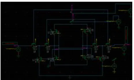
Static Random AccessMemory format[16] for electromotive force activity that ends up progressively raises mainstream. The advanced electric cell is mainly demarked to work indistinguishable trademark just as in previous 13TSRAM piece cellphone which decreases quality as well as reaches out which extended study soundness. In this advanced cell, we are introducing 21T transistors in SRAM[18] based cells. Here we introduce five different hubs: Q, QB_1, QB_2, A, and B, which accurately save at Q point. Here hub which managed by method for a couple of Complementary-MOS Schmitt[11][12] set off power circuit made up of transistors P-4, P-5, P-6, P-7, P-8, P-9, N-P-4, N-5, N-6, N-7, N-8 and N-9 is separately, passed through the levelled of in transformed measurement, put away at QB_1 and QB_2. QB_1 and QB_2
are, individually, headed in VDD along with GND by means of gadgets P-1, P-2, N-1, and N-2 that are constrained for utilizing in feeble input hubs An as well as B that which joins to Q between a couple of integral machines (P-5 and N-5) gated with the guide of QB_2. Here activity is like a 13TSRAM[17] bit cell. Be that as it may, for diminishing vitality utilization, delay and expanding analyze balance we choose 21T piece cell phone comprising of three sets Complementary-MOS as appeared in Figure.4. N-9, N-10, and N-11 are utilized in inspecting as well as compose transistors.
Fig12:13T Based Advanced SRAM
Where the measurements can be overturned at tricky hubs, it can diminish Single Event Upset's in the loop by utilizing different hubs existing in additional hardware. Thusly, we can endure agitates rather than customary 6T SRAM[17] telephone which has no input hubs. On the off chance that the wide assortment of hubs existing in the loop is additional, the realities that can never again be overturned. VDD to the diagrammatic in SRAM[18] demonstrated in Figure.5. Contrasted with the 13TSRAM piece cell, the radiant solidifying limit is extra in the 21TSRAM piece cell. Also, it postponement will moreover reduce in 13TSRAM piece mobile phone is demonstrated in figure.6.
ADVANCEDTANNER CIRCUIT:
Fig12:13T Based Advanced SRAM in Tanner 32nm
Fig13:13T Based Advanced SRAM simulation in 32nm
ADVANCED DSCH CIRCUIT:
Fig14:13T Based Advanced SRAM in Tanner 32nm
ADVANCED LAYOUT:
Fig15:13T Based Advanced SRAM Layout32nm
ADVANCED LAYOUT POWER
Fig16:13T Based Advanced SRAMsimulation32nm
II.
RESULTS
AND
COMPARISON
It shows the intensity of 6TSram, 13TSram, proposed 21TSram piece cell and 21T Sram piece cell with various
supply electromotive forces. In this table how a decrease in the control of various topologies. From that table, it can clarify the 21TSram piece cell is the best elective topology than 6TSram and 13TSram piece cells.
TABLE IPOWER AT DIFFERENT SUPPLY VOLTAGES:
Leakage Power 0.35v
6T SRAM Bit Cell 7nW
13T SRAM Bit Cell 1nW
ADVANCED SRAM
Bit Cell 0nW
Table:1 Leakage power Statistics
A.THEORETICAL CALCULATIONS:
The normal power dissemination of various topologies utilized in this paper is hypothetically determined by the condition (1)
P 2 n— (1) avg LDD
VDD = Voltage supply (800mV), CL = Capacitance of load, F = Frequency of information, n = No. of transistors.
Fig17: Graphical representation of Leak power
conclusion
This paper proposes a 21T based SRAM bit cell, intended for vigorous, low-voltage, Ultra-low power approach. The advanced circuit shows a hardback double determined isolated criticism instrument with double CMOS Schmitt trigger inverter with numerous stockpile voltages to accomplish high delicate blunder resistance, for strong activity down to 500 mV. Molecule strike concealment was done, demonstrating resistance to upsets up to 500-mV working voltage. Power utilization diminished from 7nW.
References
[1] A. Wang, B. H. Calhoun, and A. P. Chandrakasan, ―Sub- Threshold Design for Ultra-Low-Power Systems (Series on Integrated Circuits and Systems)‖. Secaucus, NJ, USA: Springer-Verlag, 2006.
[2] T. Heijmen, D. Giot, and P. Roche, ―Factors that impact the critical charge of memory elements‖, in Proc. IEEE Int. Symp. (IOLTS), Jul. 2006, pp.16. [3] S. Fisher, A. Teman, D. Vaysman, A. Gertsman, O.
Yadid- Pecht and A. Fish, ―Digital sub-threshold logic designs Motivation and challenges‖, in Proc. IEEE Conv. Elect. Electron. Eng. Israel (IEEE), Dec. 2008, 0
1 2 3 4 5 6 7
1471
pp.702-706.
[4] C. Detcheverry et al., ―SEU critical charge and sensitive area in a submicron CMOS technology‖, IEEE Trans. Nucl. Sci., vol. 44, no. 6, pp. 2266-2273, Dec.1997.
[5] R. C. Baumann, ―Radiation-induced soft errors in advanced semiconductor technologies‖, IEEE Trans. Device Mater. Rel., vol. 5, no. 3, pp. 305316, Sep.2005.
[6] T. Karnik and P. Hazucha, ―Characterization of soft errors caused by single event upsets in CMOS processes‖, IEEE Trans. Dependable Secure Comput., vol. 1, no. 2, pp. 128- 143, Apr./Jun.2004. [7] B. H. Calhoun and A. P. Chandrakasan, ―A 256-kb
65-nm sub-threshold SRAM design for ultra-low-voltage operation‖, IEEE J. Solid-State Circuits, vol. 42, no. 3, pp. 680-688, Mar.2007.
[8] LiorAtias, Adam Teman, Robert German, Pascal Meinerzhagen and Alexander Fish, ―A Low-Voltage Radiation-Hardened 13T SRAM Bit cell for Ultralow Power Space Applications‖, IEEE transactions on (VLSI) systems, vol. 24, no. 8, Aug. 2016, pp.2622-2633.
[9] L. Sterpone and M. Violante, ―Analysis of the robustness of the TMR architecture in SRAM-based FPGAs‖, IEEE Trans. Nucl. Sci., vol. 52, no. 5, pp. 1545-1549, Oct.2005.
[10]T. Calin, M. Nicolaidis and R. Velazco, ―Upset hardened memory design for submicron CMOS technology‖, IEEE Trans. Nucl. Sci., vol. 43, no. 6, pp.2874-2878, Dec.1996.
[11]Ahdal, A. A. Toumazou, C. (2012). ―ISFET-based chemical Schmitt trigger. Electronics Letters‖, 48(10), pp.549-551.
[12]Dokic, B. L. (1996). ―CMOS NAND and NOR Schmitt Circuits‖, Micro-electronics Journal, 27(8),pp.757-765.
[13]Kulkarni, J. P., Kim and Roy. K. (2007), ―A 160 mV robustSchmitttriggerbasedsub-threshold SRAM‖, IEEE
[14]J. Solid-State Circuits, 42(10), pp.2303-2313. [15]Lotze, N., and Manoli, Y. (2012), ―A 62 mV 0.13 m
CMOS Standard-Cell-Based Design Technique Using Schmitt-Trigger Logic‖, IEEE Journal of Solid-State Circuits, 47(1),pp.47-60.
[16]Kumar, M. S., Inthiyaz, S., Vamsi, C. K., Ahammad, S. H., Sai Lakshmi, K., VenuGopal, P., &BalaRaghavendra, A. (2019). Power optimization using dual SRAM circuit. International Journal of Innovative Technology and Exploring Engineering, 8(8), 1032-1036.
[17]Siva Kumar, M., Inthiyaz, S., Venkata Krishna, P., JyothsnaRavali, C., Veenamadhuri, J., Hanuman Reddy, Y., & HasaneAhammad, S. (2019). Implementation of most appropriate leakage power techniques in VLSI circuits using NAND and nor gates. International Journal of Innovative Technology and Exploring Engineering, 8(7), 797-801
[18] KVS Sree Sailajaa Vidyadhari, Sanath Kumar Tulasi. Design ALU Based online BIST for Multi Word-Width RAM’s. International Journal of Innovative Technology and Exploring Engineering,
vol(2), pp-24 -32,(2015)