A GENERALIZED DESIGN PROCEDURE FOR A
MICROWAVE AMPLIFIER: A TYPICAL APPLICATION EXAMPLE
F. G¨une¸s andC. Bilgin
Electronics and Communication Engineering Department Yıldız Technical University
Be¸sikta¸s, Istanbul, Turkey
Abstract—In this work, a generalized procedure is carried out for the design of a microwave amplifier. First of all, the Performance Data Sheets (PDS) resulted from the active device characterization are used as Feasible Design Target Space (FDTS). Employing the PDS, the compatible (Noise F, Input VSWR Vi, Gain GT) is determined
over the predetermined bandwidthB betweenfmin andfmaxoperation
frequencies with the sourceZS and loadZLterminations as the design
target. In the design stage, the Simplified Real Frequency Technique (SRFT) is utilized in the scattering-parameter formulation of the front- and back-end matching two-ports to provide the source and load terminations to the transistor, respectively. As an application example, a novel high technology transistor is chosen and the design targets are determined using the PDSs of the device and its front-and back-end matching two-ports are characterized by the scattering-parameters using the novel SRFT for each design target. Furthermore, the performances of the resulted amplifier circuits are analyzed and compared with the simulated results.
1. INTRODUCTION
(LNA)s together with the 50 Ω noise match, a high gain along ultra-wide bandwidth (UWB). Recently, typical design works [1, 2] with SiGe heterojunction bipolar transistors are presented in the literature compatible with conventional low-cost Si CMOS [3] manufacturing for these requirements. Besides, an UWB design is presented in [4] employing LC ladder matching networks for a 3–10 GHz on-chip SiGe LNA amplifier.
Among the major problems observed in these types of studies is the lack of the “Feasible Design Target Space (FDTS)”. In the other words, design process must be performed using the physical limits and/or compromise relations within the design hexagon consisting of bias voltageVDS, bias currentIDS, noiseF, gainGT, input VSWRVi,
operation bandwidthB. This problem has not solved yet by the today’s computer aided analysis and synthesis tools for RFICs, which are still in their infancy, forcing the designer to rely on experience, intuition or inefficient simulation techniques to predict the performance. It should also be noted that optimization process of the amplifier performance is highly nonlinear in terms of the descriptive parameters of the system. Certainly, within the optimization process, one can easily embed the desired performance goals without knowing the physical limits and/or compromise relations among noise (F), input VSWR (Vi) and gain
(GT) appropriately. Unfortunately this process often fails to attain
the desired goals.
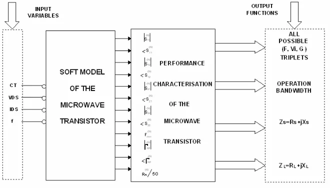
The physical limits and/or compromise relations within the design hexagon may be carried out in a systematic manner into the Performance Data Sheets (PDS) of the device and can be obtained in the following main stages as given in Fig. 1: (i) Firstly, a Soft-Model of the transistor which may be either Neural [5] or Support Vector model [6], is generated to determine the signal and noise behaviors within the whole operation domain of the device consisting of the configuration type (CT), the bias condition VDS, IDS, the operation
frequency f; (ii) Secondly, noise, input VSWR, gain performance of the device is characterized point by point within the operation domain as given in the works [7, 8]; (iii) Finally, the Performance Data Sheets (PDS) can be obtained as resulted from the Gain-Bandwidth limitations [9] using the performance characterization of the active device.
multilayer cylindrical coplanar lines [10], calculation of the impedance of air-suspended trapezoidal and rectangular shaped microshield lines [11], non uniform antenna array synthesis [12], design of the coplanar waveguides combining fuzzy systems [13], passive dipole arrays with together genetic algorithm [14]. On the other-hand, support vectors have become a strong competent method to the neural networks by the typical applications on the linear- [15] and non linear modeling [16] of mesfets; modeling of the microwave devices such as microstrip antenna based on the experimental data [17], mim capacitors [18].
The whole process is applied in a recent work [19] in details in the designof a LNA amplifier with together gradient-based method, where all the other pioneer works for the circuit-based stage are included and T-, Π-, L-types of the distributed-parameter matching networks are employed. Furthermore evolutionary algorithms such as genetic, very fast simulated reannealing and particle swarm algorithms are also utilized in [20–22] to optimize the distributed parameters of theT-, Π-, L-types of the matching networks subject to the PDS of the device.
In this work, the similar design procedure to the one in [19–22] is followed and worked out to put forward a general procedure for the design of a microwave amplifier with a different type of the modeling for the transistor terminations’ data, as independent of the circuit topology. To the authors’ knowledge, these are expected to contribute the following originalities into the literature: (1) The Feasible Design Target Space (FDTS) based upon the Gain-Bandwidth limitations of the employed active device [9] is used, thus the compatible (F,Vi,GT)
triplet is chosen to supply as the performance target with together its corresponding operation bandwidth B into the design process. This type of determination of the FDTS results in these advantages: (i) Input VSWR Vi is also introduced as a free variable into the design
procedure; Furthermore, (ii) Stability of the device does not need to be considered as an additional target, since all the solution terminations take place within the Unconditionally Stable Working Area (USWA) of the device [7, 8]; (iii) Each component of the Compatible (F, Vi,
GT) triplet may also be chosen as a function of frequency, i.e., one
of our choices is that Freq = 0.46 dB; Vi = 1 and GTmax(f) which
is the constrained maximum gain at each operation frequency along the operation bandwidth B as given in Fig. 6. Another frequency dependent choice may be in the form ofFreq=Fmin(f),Vireq =const.,
GTmax(f), where GTmax(f) is the maximum gain at each operation
frequency constrained by the requirements of Freq = Fmin(f) and
Vireq =const. (2) The multi-objective design of the whole amplifier is
finally simplified as modeling of the targetZS,ZL terminations’ data
topology. A reflectance based real-frequency technique [23] is employed in the modeling using theLandC elements within the practical range. Furthermore, since the reference source and load impedances may be chosen as 50 Ω, so there is no need for the diplexer to provide 50 Ω for source and/or load. So this will help to reduce the size for the miniaturization.
In the following sections, block diagram for the Performance Data Sheets in the Fig. 1 will be considered block by block in an order. In the later sections, the reflectance-based type of the data modeling for the terminations will briefly be given together with optimization algorithms and applications.
Figure 1. A block diagram for the performance data sheets.
2. PERFORMANCE DATA SHEETS OF A MICROWAVE TRANSISTOR
2.1. Potential Performance of a Microwave Transistor: Compatible (F, Vi, GT) Triplets and (ZS, ZL) Terminations
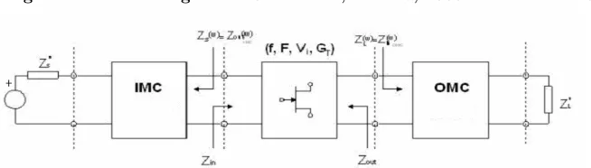
A typical design problem of a basic microwave amplifier employing per se, a GaAs FET as an active device is given by Fig. 2.
Since in such a system, all the main performance components of F,Vi, GT can be determined by the active device employed, so it has
to be identified by all its possible (F, Vi,GT) triplets and their (ZS,
Figure 2. Microwave transistor with the matching circuits for the potential characteristics.
All the compatible (F, Vi, GT) triplets are the simultaneous
solutions of the following three nonlinear performance equations for the passive (ZS, ZL) terminations in the operation domain of the active
device:
GT =
PL
PAV S
=G{RS, XS, RL, XL}
= 4RSRL
|(z11+ZS) (z22+ZL)−z12z21|2
(1)
F = (S/N)i
(S/N)o=F{RS, XS}=Fmin+ RN
|Zopt|2
|ZS−Zopt|2
RS
(2)
Input VSWR =Vi =Vi{RS, XS, RL, XL}=
1+|ρi|2
1−|ρi|2
, ρi=
ZS−Zi∗
ZS+Zi∗
(3)
The solution subsets {ZS, ZL/Rs>0, RL>0} in which we are
interested, are the sets that ensure stable working of the transistor within its physical limitations, thus they have to satisfy the following inequities and/or equalities:
Re{Zi}>0, Re{Zo}>0 (4)
GTmin ≤GT ≤GTmax, Vi ≥1, F ≥Fmin (5)
where Zi and Zo are the input and output impedances of the active
device two-port, respectively, which are in terms of [z] parameters are,
Zi=z11−
z12z21
z22+ZL
, Zo =z22−
z12z21
z11+ZS
(6)
The problem of the gain limitations can be described as a mathematically constrained extremum problem, which is to find the extremum stable values of the function G{RS, XS, RL, XL} in (1)
subject to
This constrained extremum problem and determination of the (ZS, ZL) terminations ensuring any GT value between the GTmin ≤
GT ≤ GTmax are rigorously solved by the linear circuit and noise
theory using impedance [z] — or scattering [S]-parameter approach in [7, 8] respectively and employed to obtain the PDSs for the potential performance of the microwave transistor.
In the next subsection ‘Performance Data Sheets’ will be dealt to be used in the design of the front- and back-end matching circuits.
2.2. Performance Data Sheets
PDSs of a microwave transistor can be obtained from the block diagram given in Fig. 1 which consists of the two main parts: (i) The first part is “The Data-Based Soft” model of the device which needs some amount of data to be established. In this part, linear learning machines such as neural network [5], or support vector machine [6] can be employed; (ii) The second part is ‘the Circuit Analyze-Based’ model whose fundamentals are given in the previous subsection. So PDSs can be obtained from the interrelations among the physically realizable performance triplets and terminations over a defined operation bandwidthB, expressed as follows:
Freq, Vireq, GTmax
⇔ ZSmax =RSmax+jXSmax;
ZLmax =RLmax+jXLmax
(7a)
Freq, Vireq, GTmin
⇔ ZSmin =RSmin+jXSmin;
ZLmin =RLmin+jXLmin
(7b)
Freq, Vireq, GTreq
⇔ ZSreq =RSreq+jXSreq;
ZLreq =RLreq+jXLreq
(7c)
In the worked examples, PDSs of a high technology transistor is considered to obtain the design target space for the microwave amplifier circuits.
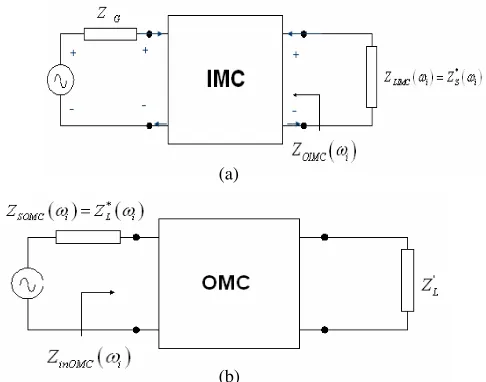
We can have the two alternative approaches in formation of the design target space from (7a), (7b) and (7c) to employ either (i) the compatible (F, Vi, GT) triplets for the whole amplifier circuit or (ii)
the ZS and ZL terminations for the input (IMC) and output (OMC)
3. REFLECTANCE BASED REAL-FREQUENCY TECHNIQUE TO MODEL THE COMPUTED BR TERMINATION DATA
3.1. Scattering Parameter Characterization of the Matching Networks
In this work, the Reflectance Based Method is employed, whose essentials are based upon the simplified real frequency technique given in details [13], to build up the scattering parameters of the Darlington two-ports to match the given generator ΓG and load Γr
terminations to the required source ΓS and load ΓL terminations of
the transistor, respectively, for the desired (F, Vi, GT) triplets, as
given in the Figs. 2–3. In our approach, the modeling problem can be defined as the generation of a realizable bounded real (BR) reflectance function which best fits the given data. Eventually, this BR reflectance is synthesized as a lossless and reciprocal “Darlington two-port” in resistive termination, yielding the desired circuit model. Obviously, the solution is not unique. The goal is, to end up with a reasonable BR reflectance function such that the resulting circuit can be built easily with least number of elements. In the course of the modeling, the termination data is examined and the corresponding BR reflectance forms are selected carefully.
(a)
(b)
Let S(ωi) = SR(ωi) +jSX(ωi) or S(ωi) = ρ(ωi)ejφ(ωi) be the
given reflectance data such thatρ(ωi)≤1 over the sample frequencies
ωidefined throughout the operation bandwidthB. Let{Skl;k, l= 1,2}
designate the scattering parameters of the corresponding model which defines a lossless, reciprocal two-port, so called “Darlington two-port”. For a lumped element, reciprocal, lossless two-port, the scattering parameters may be expressed in the Belevitch form as follows:
S11(s) =
h(s)
g(s);S21 (s) =S12(s) = f(s)
g(s);S22 (s) =−
f(−s)h(−s) f(s)g(s)
(8a) In (8a),s=σ+jω designates conventional complex domain variable associated with lumped elements,g(s) is annth degree strictly Hurwitz polynomial with real coefficients such that
g(s) =gnsn+gn−1sn−1+. . .+g2s2+g1s+g0 (8b)
Similarly, h(s) is also an nth degree polynomial with free real coefficients hi. That is,
h(s) =hnsn+hn−1sn−1+. . .+h2s2+h1s+h0 (8c)
In (8a), f(s) is a real polynomial which includes all the transmission zeros of the termination under consideration. Furthermore, the losslessness condition requires that S(s)S(−s) =I, which necessitates the following relation between the Belevitch polynomials:
g(s)g(−s) =h(s)h(−s) +f(s)f(−s) (9a) This also imposes the following degree relations:
degh≤n,degf ≤n wheren= degg. (9b) Based on the above explanation, the termination reflectance data — ΓS(jωi) or ΓL(jωi) — must be equal to the input scattering
coefficientS1l(jωi) of the Darlington two-port to provide matching to
the transistor. Losslessness condition of (9a) requires that ρ221(ωi) =
1−ρ2(ωi)≤1;∀ωi, whereρ is the magnitude of the Siis. So, once an
appropriate form off(s) is selected, we can generate the full scattering parameters of the lossless and reciprocal Darlington two-port from the given numerator polynomial h(s) according to the following theorem. 3.2. Main Theorem of the Reflectance — BasedModeling Problem
The scattering parameters {Skl;k, l = 1,2} of a lumped element,
numerator polynomialh(s) =hnsn+hn−1sn−1+. . .+h2s2+h1s+h0
of the input reflection coefficient S11(s) = hg((ss)) for a preselected f(s)
such that
g(jω)g(−jω) =h(jω)h(−jω) +f(jω)f(−jω) ∀ω. (10) Proof: If f(s) is preselected as stated by the theorem then, the even polynomialG(s2) =g(s)g(−s) can be constructed using (9a) in terms of f(s) and h(s) such that
G(s2) =Gns2n+Gn−1s2(n−1)+Gn−2s2(n−2)+. . .+G1s2+G0 (11)
Zeros of (11) can never be on the jω axis since g(jω)g(−jω) = h(jω)h(−jω) +f(jω)f(−jω) is never zero. Furthermore, these zeros present mirror image symmetry with respect to the imaginary axisjω. Hence, the strictly Hurwitz polynomialg(s) is constructed on the left-half plane (LHP) zeros of (11). Thus, the scattering parameters of the lossless, reciprocal two-port are uniquely determined as in (8).
3.3. Synthesis Procedure
Based on the main theorem given above, in order to ensure the fitness of the unknown real coefficients{h0, h1, h2,. . . , hn−1, hn}to the
termination data, an objective function based on “Gain Performance” of the matching networks in Figs. 3(a) and 3(b) can be used:
ε=
Nω
j=1
(1−GT(ωj, hi)), i= 1, . . . , n (12)
where Nω denotes the number of sampling frequencies over the
operation bandwidth B and the gain GT(ωj, hi) function can be
expressed in terms of the impedance mismatching factor at either port of the reciprocal, lossless matching networks such as
GT(ωj, hi) = 1− |ρ(ωj, hi)|2 (13a)
and ρ(ωj, hi) can be given in terms of the termination data for input
and output matching networks in the Figs. 3(a), 3(b), respectively, as follows:
ρIM C =
ZoutIM C(ωj, hi)−Zstr(ωj)
ZoutIM C(ωj, hi) +Zstr∗ (ωj)
(13b)
ρO M C=
ZinOM C(ωj, hi)−ZLtr(ωj)
ZinOM C(ωj, hi) +ZLtr∗ (ωj)
whereZoutIM C andZinOM C have the well-known relations in terms of
the scattering parameters of the related two-ports.
The Optimization Procedure used in this work can briefly be summarized as follows: (i) Choose a “Local Optimizer”, i.e., “Nelder-Mead Simplex” or “Gradient-based Optimizer”; (ii) Start the design of the amplifier with the differential bandwidth ⇔ narrowband from either the starting or stopping frequency of the operation bandwidth by initializing all the coefficients of the polynomialh(s) as unities; (iii) Increase the bandwidth by passing to the next sample frequency at each step and taking the previous solution set as “the initial set” to the current design and continue this procedure till reaching to the end point of the operation bandwidth.
Thus the polynomialsh(s) andg(s) are determined so that gains of the matching networks given the Figs. 3(a), 3(b) can be maximized, from (13b) and (13c) that ensure ZoutIM C ∼=ZStr, ZinOM C ∼=ZLtr at
each frequency along the operation bandwidth B. Then the bounded Scattering parameters are formed just described in (8) and the lossless and reciprocal matching circuits are synthesized using the Darlington procedure.
In the next section, the reflectance-based modeling procedure described in the above will be applied step by step to a chosen transistor NE329S01.
4. WORKED EXAMPLES
4.1. Design Target Space
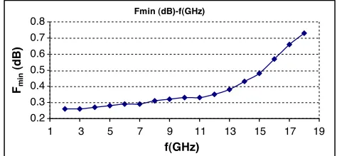
NE329S01 is chosen as the transistor to design of its front- and back-end matching two-ports, whose minimum noise profile is given by Fig. 4.
Fmin (dB)-f(GHz)
0.2 0.3 0.4 0.5 0.6 0.7 0.8
1 5 11 13 15 17 19
f(GHz)
Fmi
n
(dB)
3 7 9
Figure 5. The [0.46 dB, 1, GTmax(f)] triplet for the NE329S01
transistor.
(a)
(b)
Figure 6. (a) The source termination functions of the [0.46 dB, 1, GTmax(f)] triplet for the NE329S01 transistor. (b) The load
termination functions of the [0.46 dB, 1, GTmax(f)] triplet for the
NE329S01 transistor.
The performance characterization of the NE329S01 transistor is completed, thus for the chosen bias condition VDS = 2 V and IC =
10 mA, the maximum gain profile GTmax(f) under the constraints of
Vireq = 1⇔ conjugate matched input port,Freq = 0.46 dB is obtained
as given in Fig. 5 with together the corresponding source ZSmax(ωi)
Two design targets are chosen to be synthesized: The constrained maximum gain profile⇒(Freq = 0.46 dB,Vireq = 1, GTmax(f)) between
4 GHz and 13 GHz and the flat gain characteristic⇒(Freq = 0.46 dB,
Vireq = 1, GTreq = 12 dB) characteristics over the predetermined
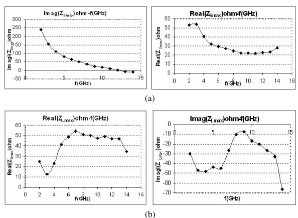
operation bandwidth 4–11 GHz from the characteristic of the Fig. 5, respectively. The terminations ZSreq(ωi), ZL(ωi), i = 1, . . . , Nω of
these targets are given in Figs. 6(a), (b) and 7(a), (b) respectively.
4.2. Synthesis Procedure
Input and output matching networks of the transistor are considered independently, as defined by Figs. 3(a) and 3(b) respectively. Choosing the low-pass circuit configuration ⇔ f(s) = 1, the real frequency technique given in the Section 3 is applied and the gains of the reciprocal and lossless matching networks are maximized using the Nelder-Mead simplex method and the two typical examples will be given below. The other many typical examples can be found in [14].
Imag(ZSreq)ohm-f(GHz )
0 40 80 120 160 200
0 2 4 6 8 10 12
f(GHz) Imag( ZSr eq )ohm (a)
Real(ZLr eq)ohm-f(GHz )
0 40 80 120 160 200 240
0 2 4 6 8 10 12
f(GHz)
Real(Z
Lre
q
)ohm
Im ag(ZLr eq)ohm -f(GHz)
-160 -120 -8 0 -40 0 40
0 2 4 6 8 10 12
f(GHz) Im a g (Z Lr e q )ohm (b)
Real(ZSreq)ohm-f(GHz)
0 20 40 60 80 100
0 2 4 6 8 10 12
f(GHz) Real(Z Sr e q )ohm
(a)
(b)
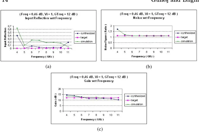
Figure 8. (a) Input matching circuit with the gain char-acteristic for the [Freq= 0.46 dB, Vireq= 1, GTreq= 12 dB] triplet
B= 4 GHz, . . . , 11 GHz of the NE329S01 transistor. (b) Output matching circuit with the gain characteristic for the
Freq = 0.46 dB, Vireq = 1, GTreq = 12 dB
(a) (b)
(c)
Figure 9. (a) Input reflection characteristics for the matching given by the Figs. 8(a) and 8(b). (b) Noise characteristics for the matching given by the Figs. 8(a) and 8(b). (c) Gain characteristics for the matching given by the Figs. 8(a) and 8(b).
4.2.1. Matching with the Design Target of (Freq= 0.46 dB, Vireq = 1,
GTreq = 12 dB) over the Operation Bandwidth (B = 4 GHz, . . . ,
11 GHz)
The Belevitch polynomials h(s) and g(s) are obtained for the input (front-end) and output (back-end) matching circuits and given in (14a)–(14b) and (15a)–(15b) respectively as follows:
hi(s) = −36.4417s8−7.2364s7−70.3068s6−19.9067s5−40.9470s4
−16.2905s3−6.8698s2−3.9457s (14a) gi(s) = 36.4417s8+ 50.3818s7+ 104.4155s6+ 98.5184s5
+91.4305s4+ 55.6473s3+ 25.3272s2+ 8.1377s+ 1 (14b)
ho(s) = −1.97s6+ 7.9986s5−0.7677s4+ 12.9658s3
+1.1402s2+ 4.7371s (15a)
go(s) = 1.97s6+ 10.0403s5+ 10.1155s4+ 17.352s3
+8.8318s2+ 6.3328s+ 1 (15b)
scattering parameters to the Belevitch polynomials given by (14a), (14b) and (15a), (15b) are given in Figs. 8(a) and (b) with together their gain characteristics, respectively.
The resulted input reflection, noise and gain characteristics of the amplifier are given as compared with target and simulation characteristics in the Figs. 9(a), (b), (c), respectively.
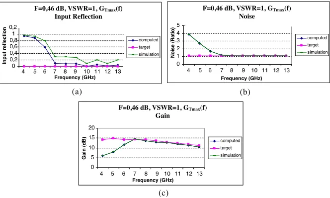
4.2.2. Matching with the Design Target (Freq= 0.46 dB, Vireq = 1,
GTmax(f)), B = 4–13 GHz
The Belevitch polynomialsh(s) andg(s) are given in (16a)–(16b) and (17a)–(17b) for the input (front-end) and output (back-end) matching
CAP
C= ID =
0.315 pF
C5 CAP
C= ID = 0.195 pF C6 IND L= ID = 0.805 nH L5 RES R= ID = 50 Ohm R2 Gain 0 0,2 0,4 0,6 0,8 1 1, 2
2 3 4 5 6 7 8 9 10 11 12 13
GHz Gain (a) Gain 0 0, 2 0, 4 0, 6 0, 8 1 1,2
2 3 4 5 6 7 8 9 10 11 12 13
GHz
Gain
(b)
Figure 10. (a) Input matching circuit with the gain characteristic by the Gain approach for theFreq= 0.46 dB, Vireq = 1, GTmax(f)
triplet B = 4 GHz, . . . , 11 GHz of the NE329S01 transistor. (b) Output matching circuit with the gain characteristic by the Gain approach for the Freq= 0.46 dB, Vireq = 1, GTmax(f)
circuits, respectively as follows:
hi(s) = −24.4533s8−24.7261s7−43.9264s6−54.2865s5
−22.8909s4−3.117s7−7.6003s (16a) gi(s) = 24.4533s8+ 49.2442s7+ 81.0095s6+ 102.0565s5
+78.7888s4+ 62.1941s3+ 23.8268s2+ 10.2675s+ 1 (16b)
h0(s) = −0.843s3−0.3742s2−0.4142s (17a)
g0(s) = 0.843s3+ 1.5901s2+ 1.8308s+ 1 (17b)
The corresponding low-pass synthesizes of the input (front-end) and output (back-end) matching circuits are given in Figs. 10(a) and (b) with together their gain characteristics.
Figures 11(a), (b), (c) denote variations of the input reflection, noise and gain with respect to the frequency for the whole amplifier circuit.
( F= 0,46 dB , VSWR = 1 , G=Maximu m ) Input Ref lect ion
0 0,2 0,4 0,6 0,8 1 0,2 Input reflection computed target simulation
F=0,46 dB, VSWR=1, GTmax(f) Input Reflection
( F= 0,4 6 dB , VSWR = 1 , G=Max imum ) Nois e 0 1 2 3 4 5
4 5 6 7 8 9
Frequency (GHz)
Noise
(Ratio) computed
target simulation
( F= 0 ,4 6 dB , VSWR = 1 , G=Maximu m ) Gain 0 5 10 15 20
4 5 6 7 8 9 10 13
Gain (dB)
computed target simulation
F=0,46 dB, VSWR=1, GTmax(f) Noise
F=0,46 dB, VSWR=1, GTmax(f) Gain
(a) (b)
(c) 11 12
10 11 1213
4 5 6 7 8 9 10 11 12 13
Frequency (GHz)
Frequency (GHz)
5. CONCLUSIONS
In this work, design of a microwave amplifier is aimed at as a generalized systematic procedure in these respects: (i) Establishment of a Feasible Design Target Space (FDTS) taking into account the physical limits and/or compromise relations within the design hexagon consisting of bias voltage VDS, bias current IDS, noise F, gain GT,
input VSWR Vi, operation bandwidth B for the used active device;
(ii) Characterization of FDTS in a convenient form to be used in Design procedure: The Performance Data Sheets (PDS) yielded from the “Active Device Characterization” stage as given in the Fig. 2, has a fairly long-working term in literature, but has found a vital application opportunity in this work; (iii) Simplification of the multi-objective design procedure of the compatible (F,Vi,GT) triplets into the design
of the sourceZS and loadZLterminations associated with the triplets.
This consists of using an impedance data modeling technique to design of the two lossless and reciprocal two-ports; (iv) The scattering-parameter formulation of the matching circuits to ensure the required (F, Vi, GT) over the predetermined bandwidth B of the transistor.
A novel impedance data modeling technique the “Simplified Real Frequency Technique (SRFT)” to is used for this purpose.
Furthermore an application example is given by choosing a novel high technology transistor where “the initial value” problem is overcome applyingN successive narrow-band design procedure taking all the initial values unities. Besides both performance analysis and simulation is made and compared to each other, and it is concluded they are agreed to each other.
REFERENCES
1. Kuo, W.-M. L., R. Krithivasan, X. Li, Y. Lu, J. D. Cressler, H. Gustat, and B. Heinemann, “A low-power, X-band SiGe HBT low-noise amplifier for near-space radar applications,”IEEE
Microwave and Wireless Components Letters, Vol. 16, No. 9, 520–
522, Sept. 2006.
2. Park, Y., C.-H. Lee, J. D. Cressler, and J. Laskar, “Theoretical analysis of a low dispersion SiGe LNA for ultra-wideband applications,”IEEE Microwave and Wireless Components Letters, Vol. 16, No. 9, 517–519, Sept. 2006.
3. Bevilacqua, A. and A. M. Niknejad, “An ultrawideband CMOS low-noise Amplifier for 3.1–10.6-GHz wireless receivers,” IEEE
Journal of Solid-state Circuits, Vol. 39, No. 12, 2259–2268,
4. Ismail, A. and A. A. Abidi, “A 3–10-GHz low-noise amplifier with wideband LC-ladder matching network,”IEEE Journal of
Solid-state Circuits, Vol. 39, No. 12, 2269–2277, Dec. 2004.
5. G¨une¸s, F., H. Torpi, and F. G¨urgen, “A multidimensional signal-noise neural model for microwave transistor,”IEE Proc. Circuits
Devices System, Vol. 145, No. 2, 111–117, 1998.
6. G¨une¸s, F., N. T¨urker, and F. G¨urgen, “Signal-noise support vector model of a microwave transistor,” accepted for publication inInt.
J. RF Microwave CAE, July 2007.
7. G¨une¸s, F., M. G¨une¸s, and M. Fidan, “Performance characteriza-tion of a microwave transistor,” IEE Proc. Circuits Devices Sys-tem, Vol. 141, No. 5, Oct. 1994.
8. G¨une¸s, F. and B. A¸cetiner, “Smith chart formulation of performance characterization for a microwave transistor,” IEE
Proc. Circuits Devices System, Vol. 145, No. 6, Dec. 1998.
9. G¨une¸s, F. and C. Tepe, “Gain-bandwidth limitations for a microwave transistor,”Int. J. RF Microwave CAE, Vol. 12, No. 6, 483–495, 2002.
10. Yildiz, C. and M. Turkmen, “Quasi-static models based on artificial neural networks for calculating the characteristic parameters of multilayer cylindrical coplanar waveguide and strip line,”Progress In Electromagnetics Research B, Vol. 3, 1–22, 2008. 11. Guney, K., C. Yildiz, S. Kaya, and M. Turkmen, “Artificial neural networks for calculating the characteristic impedance of air-suspended trapezoidal and rectangular-shaped microshield lines,”
J. of Electromagn. Waves and Appl., Vol. 20, No. 9, 1161–1174,
2006.
12. Ayestar´an, R. G., F. Las-Heras, and J. A. Mart´ınez, “Non uniform-antenna array synthesis using neural networks,” J. of
Electromagn. Waves and Appl., Vol. 21, No. 8, 1001–1011, 2007.
13. Turkmen, M., S. Kaya, C. Yildiz, and K. Guney, “Adaptive neuro-fuzzy models for conventional coplanar waveguides,” Progress In
Electromagnetics Research B, Vol. 6, 93–107, 2008.
14. Ayestar´an R. G., J. Laviada, and F. Las-Heras, “Synthesis of passive-dipole arrays with a genetic-neural hybrid method,” J. of
Electromagn. Waves and Appl., Vol. 20, No. 15, 2123–2135, 2006.
15. Xu, Y., Y. Guo, R. Xu, and Y. Wu, “Modeling of SIC MESFETs by using support vector machine regression,” J. of Electromagn.
Waves and Appl., Vol. 21, No. 11, 1489–1498, 2007.
Progress In Electromagnetics Research Letters, Vol. 2, 103–114, 2008.
17. Tokan, N. T. and F. G¨une¸s, “Support vector characterization of the microstrip antennas based on measurements,” Progress In
Electromagnetics Research B, Vol. 5, 49–61, 2008.
18. Yang, Z. Q., T. Yang, Y. Liu, and S. H. Han, “MIM capacitor modeling by support vector regression,”J. of Electromagn. Waves
and Appl., Vol. 22, No. 1, 61–67, 2008.
19. G¨une¸s, F. and S. Demirel, “Gain gradients applied to optimization of distributed parameter matching circuits for microwave transistor subject to its potential performance,” accepted for publication in Int. J. RF Microwave CAE, Vol. 18, No. 2, 99– 111, Mar. 2008.
20. G¨une¸s, F. and Y. Cengiz, “Optimization of a microwave amplifier using neural performance data sheets with genetic algorithms,”
Lecture Notes in Computer Science, 630–637, 2003.
21. Cengiz, Y., H. G¨oksu, and F. G¨une¸s, “Design of a broadband microwave amplifier using neural performance data sheets and very fast simulated reannealing,” Lecture Notes in Computer
Science, Vol. 6, No. 2, 815–820, 2006.
22. Demirel, S., F. G¨une¸s, and U. Ozkaya,¨ “Particle swarm intelligence applied to design microwave amplifier for the maximum gain constrained by the minimum noise over the available bandwidth,” Submittedto Progress In Electromagnetics Research.
![Figure 7. (a) The source termination functions of the [0.46 dB, 1,12 dB] triplets for the NE329S01 transistor](https://thumb-us.123doks.com/thumbv2/123dok_us/1903854.1249333/12.612.95.430.312.540/figure-source-termination-functions-db-triplets-ne-transistor.webp)