Shared-Aperture Dual-Band Dual-Polarization Array Using
Sandwiched Stacked Patch
Zhu Sun1, 2, *, Karu P. Esselle1, Shun-Shi Zhong2, and Yingjie J. Guo3
Abstract—An L/C dual-band dual-polarized (DBDP) shared aperture microstrip array is proposed in the paper. In the array, the novel sandwiched stacked patch structure is proposed and employed to improve lower band bandwidth for given antenna thickness. Several key issues regarding the proposed structure are discussed, including: 1) merits of proposed sandwiched stacked patch structure; 2) C-band feeding method; 3) radiation performance in both bands. A prototype array of L/C DBDP sandwiched stacked patch is designed and fabricated to verify the feasibility of the proposed structure, where the measured data are presented in the paper.
1. INTRODUCTION
Dual-band dual-polarization (DBDP) antenna array can operate on two far separated bands with minimized aperture size. This ability makes it attractive for some applications requiring low weight and small size, such as space-borne SAR systems.
The perforated microstrip patch array is a special type of interleaved structure, and it is one of the most commonly used methods for DBDP antenna [1–15]. Refs. [1, 2] present the experiment results of two perforated patch DBDP arrays operating at L/C and L/X band, respectively. From the best of the authors’ knowledge, they are the earliest literatures that comprehensively explain the principals of perforated DBDP microstrip patch array. Bandwidths of 7% are achieved in both bands of two arrays, which are very good results when considering that the antenna profiles are only about 8 mm. Similar perforated DBDP arrays are continuously reported since then. Within these reports, a best bandwidths of 13% and 16% are achieved at lower and higher bands, at the expense of increasing antenna profile to 24.5 mm [3, 4].
The overlapped structure [16, 17], which places the higher band elements above the lower band stacked patch, can completely avoid the perforation on lower band stacked patch. Bandwidth of lower band element is thus improved for the specified L-band element thickness. However, the overall profile of overlapped structure DBDP array is composed of lower and higher band element thicknesses, and thus, makes overlapped structure slightly thicker than perforated patch.
The paper proposes a novel L/C sandwiched stacked patch DBDP microstrip array, which aims at lower band bandwidth improvement for the specified antenna thickness. A prototype array is designed and fabricated to verify the feasibility and merits of the proposed structure. The requirements of the array are listed in Table 1.
The paper is organized as follows. Section 2 gives the analysis between perforation and bandwidth, and proposes a novel sandwiched stacked patch structure for a dual-band array. Section 3 presents a sandwiched stacked patch DBDP prototype array as well as some related design skills. The experimental results are given in Section 4. Section 5 concludes the pros and cons of the proposed structure.
Received 21 May 2014, Accepted 4 August 2014, Scheduled 20 August 2014
* Corresponding author: Zhu Sun ([email protected]).
Table 1. Requirements of L/C sandwiched stacked patch DBDP array.
L-band C-band
Center frequency 1.25 GHz 5.5 GHz
Bandwidth 150 MHz 600 MHz
Polarization dual-linear dual-linear
Cross-polarization −25 dB −25 dB
Polarization isolation 25 dB 25 dB
Scan range ±25◦ in two dimension ±25◦ in two dimension
2. PERFORATION & BANDWIDTH
The space-borne SAR antenna, which is an important application for DBDP shared aperture array, requires both wide bandwidth and low antenna profile for distance resolution and easy stowing purpose. However, wide bandwidth requires low elementQfactor, which is generally realized by employing thicker resonant cavity in element design. This is very tough for lower band elements of a DBDP array, because the profile of a DBDP array is commonly decided by the lower band element thickness; therefore, it is necessary to study how to improve the antenna bandwidth with the specified thickness.
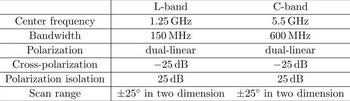
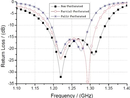
Reference [5] pointed out that element bandwidth is inversely proportional to perforation size in perforated patch. To intuitively understand relationship between bandwidth and perforation in the stacked patch, a numeric comparison is made among non-perforated, partial-perforated and fully-perforated stacked patches, as shown in Fig. 1. To exclude the disturbance of other factors, parameters which may affect bandwidth are fixed, including substrate material (Rogers 4003C), feeding method (coplanar feed), element profile (0.074λ0) and perforation shape. The in-band ripple factor is also tuned to same level (−15 dB) for the design margin.
(a) Stacked patch (b) Partial perforated patch (c) Fully perforated patch
Figure 1. Configurations of stacked patch with different perforation.
The parameters (defined in Fig. 1) of three structures are optimized by commercially available software Ansoft HFSS 13.0, and they are listed in Table 2 for reference. The predicted |S11| ≤
−10 dB bandwidths of stacked patch, partial perforated stacked patch and fully perforated stacked patch are 164 MHz (1177 ∼ 1341 MHz, 13.0%), 133 MHz (1185 ∼ 1318 MHz, 10.6%) and 104 MHz (1194 ∼ 1298 MHz, 8.3%), respectively, as shown in Fig. 2. A clear trend is observed that element bandwidth decreases with the increase of perforation numbers.
3. SANDWICHED STACKED PATCH ARRAY
Figure 2. Relationship between bandwidth and perforation.
Table 2. Parameters of three type stacked patch.
Classical Perforated Patch
Pa 74 Pb 90 h1 3.048
D 5 fw 6 ht 17.861
ls 49
Partial Perforated Stacked Patch
Pa 74 Pb 81 h1 3.048
D 5 fw 6 ht 17.861
ls 51 P1 26 d2 36
Fully Perforated Stacked Patch
Pa 68 Pb 79 h1 4.572
D 10 fw 9 ht 17.861
ls 50 P1 26 d2 36
P2 26 d3 36
stacked patch as lower band element. Although it can take full use of the given thickness to broaden lower band element bandwidth, the overall profile of overlapped DBDP antenna is a bit higher, because its profile is composed by both lower and higher element thicknesses.
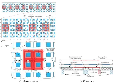
A novel sandwich structure L/C DBDP antenna is proposed for both bandwidth and low profile consideration, as shown in Fig. 3. Partial-perforated stacked patch is applied as L-band radiator. C-band stacked patches are configured between the L-C-band driven and parasitic patches, while L-C-band driven patch serves as the ground plane of C-band element. The perforations on L-band driven patch are avoided, which is helpful to improve bandwidth. Because C-band elements are contained in L-band cavity, no extra space is required like overlapped structure. Low profile characteristic is thus remained. This structure is actually a tradeoff between perforated patch and overlapped structure. The design details are illustrated as below.
3.1. Full Array Design
(a) Sub array layout (b) Cross view
Figure 3. Schematic diagram of sandwiched DBDP array.
the reasons are:
The sub array for SAR antenna should be extendable, since SAR antenna commonly has a large aperture. However, in this design, every 2×2 C-band element constructs an inseparable periodical structure, and L/C-band element numbers should keep scale to the frequency ratio to avoid grating lobe (as will be discussed). Subarray partition should stick to L/C-band elements quantity ratio and frequency ratio, to ease the subarray extension, as shown in Fig. 3(a). The asymmetric configured subarray in Fig. 3 is thus formed.
The asymmetric aperture will give minor effect on C-band overall radiation patterns due to its electric large scale aperture. The L-band radiation patterns will suffer from asymmetry due to the limited element numbers; however, this side effect will be eliminated with the enlarging of aperture, which is the common case of SAR antenna.
3.2. Subarray Design
In C-band array, larger element space is desired, because it can leave more room for L-band element, which is helpful to dual-band elements embedding and sub-array partition. The triangle distribution can cover 13% more area than the square distribution; however, the square lattice is employed for C-band because it is compatible to the L-band square driven patch on which C-band elements will overlap. The element distance for square distribution can be decided simply by:
dc =λH/(1 + sinθ) = 36 mm (1)
The L-band elements are also square distributed to ease subarray partition. The element distance is restricted by two factors: 1) scan requirement, which can be decided by:
d≤λH/(1 + sinθ)≤156 mm (2)
whereλH is the free space wavelength of 1.35 GHz. 2) To ease the L- and C-band elements embedding,
the L/C-band element distance ratio is set to an integer number. In this design,dL/dC = 4 is employed,
corresponding to 144 mm forL band element distance. Please refer to the subarray layout in Fig. 3.
3.3. C-Band Element Design
Square stacked patch [18] is employed for C-band elements for both bandwidth and compact structure consideration. The C-band driven patch and microstrip feed line are configured at the upside of layer #1, where the parasitic patches are etched on the bottom side of layer #2, as shown in Fig. 3(b).
The C-band driven patches are coplanar fed at adjacent edges for dual linear polarization. A unit cell is formed by 2×2 C-band elements. For expense reason, two adjacent co-polarized ports are combined before vertical feeding to reduce connector, coaxial line and power divider number, as shown in Fig. 3(a). The feed lines are then focused at the center of unit cell and vertically get through the L-band cavity there. The vertical feeding will be introduced shortly. Pair-wise anti-feeding technique [19, 20] is employed in each unit cell to improve the cross-polarization performance, as shown in Fig. 3(a).
The 2×1 arraying will definitely limit antenna’s scan capability in one dimension; however, the H-port scan range in horizontal plane (defined in Fig. 3(a)) is almost not impacted. Considering that the prototype array is only used for idea and specification verifying, this design is still reasonable.
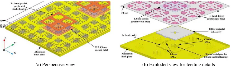
To uniform the C-band array, C-band elements outside the L-band cavity employ the same design as those sandwiched in L-band cavities. Moreover, the outside C-band elements are elevated to the same level as those embedded in L-band elements, as shown in Fig. 3(b). In other words, the L-band lower cavity digs into the back plate, as shown in Fig. 4(b).
(a) Perspective view (b) Exploded view for feeding details
Figure 4. Configuration of sandwiched DBDP sub array.
3.4. L-Band Element Design
The square partial perforated stacked patch is applied to L-band element due to the advantages aforementioned. The back plate is dug in to form L-band driven patch’s resonant cavity, as shown in Fig. 4(b). The Rogers 4003 substrates are filled into the cavity in order to reduce L-band element thickness. The L-band driven patches are etched on the bottom side of layer #1, while the parasitic patches are located at the downside of layer #3, as shown in Fig. 3 and Fig. 4.
1.15 1.20 1.25 1.30 1.35 -50
-40 -30 -20 -10 0
l1
l
2
Metal Post
L patch
|
S
21
| / (dB
)
Frequency / (GHz)
l1/l2=22/16
l1/l2=22/17 l1/l2=22/18 l1/l2=24/17
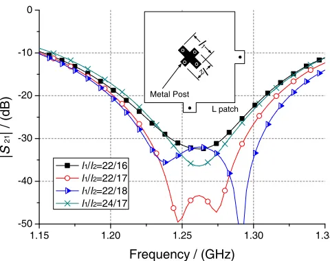
Figure 5. Parameter study on metal post shape and isolation.
Fig. 4(b). By tuning the length of two cross armsl1 andl2 (defined in Fig. 5), the polarization isolation can be suppressed. The parameter study of arm length is presented in Fig. 5. The perturbation will also raise element cross polarization level; however, it can be suppressed by applying pair-wise anti-phase feeding method [19, 20] in the array scale.
C-band elements vertical feeding is a key issue for L-band element design. The vertical feeding should get through the cavity of L-band driven patch and then feed the C-band elements overlapped on. Considering that the L-band square patch operating at the dominant mode TM01, the E-field distribution has a null point at the patch center for both polarizations, vertical feeding at this point will introduce minimal interference to the L-band cavity. Ref. [23] presents several cavity cross over structures, where direct connectors cross over is most suitable for this design, because we can best use the metal perturbation in the center of L driven patch cavity, as shown in Fig. 3(b) and Fig. 4(b). The C-band SMA connectors get through the L-band cavity via the ‘shaped metal post’ in the patch center, and then feeding the C-band element through microstrip line.
3.5. L/C-Band Elements Embedding
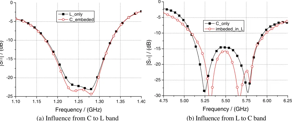
The C-band elements are embedded between L-band driven patches and perforated parasitic patch. The L driven patch also serves as the ground plane, and parasitic patches are perforated to avoid shielding C-band radiation, as shown in Fig. 3. Literally, the C-band elements are sandwiched in L-band cavities. A concern is whether L- or C-band elements performance will suffer from the embedding of other band elements in L/C DBDP sandwiched stacked patch structure. To study inter-band isolation, a numeric comparison is made between stand-alone and embedded elements in terms of the port return loss, as shown in Fig. 6.
From the prediction, C-band elements have little impact on L-band bandwidth. This is probably because C-band elements dimension are much smaller than L-band half wavelength, which means that the radiated energy from L-band patch is very difficult for C-band element to couple.
The L-band elements slightly introduce some influences on C-band elements. The bandwidth and frequency range of embedded C-band patch keep consistency with that of standalone patch, while some small difference for in-band ripples can be observed, as shown in Fig. 6.
Good inter-band isolation grants us great convenience in the design. The elements of each band can be designed independently and put together without seriously degrading the electrical performance. This point is helpful for reducing the calculation load and time consumption in simulation.
1.10 1.15 1.20 1.25 1.30 1.35 1.40 -25
-20 -15 -10 -5 0
|S
11
| /
(
d
B)
Frequency / (GHz)
L_only C_embeded
4.75 5.00 5.25 5.50 5.75 6.00 6.25
-30 -25 -20 -15 -10 -5 0
|S
11
| / (dB)
Frequency / (GHz)
C_only imbeded_in_L
(a) Influence from C to L band (b) Influence from L to C band
Figure 6. Influence from inter-band coupling.
4. EXPERIMENTAL RESULTS
An L/C DBDP sandwiched stacked patch subarray, comprising 4×1 L-band elements and 16×6 C-band elements, is fabricated and measured to validate the design, as shown in Fig. 7. Due to the budget reason, only one subarray is fabricated.
The antenna return loss is measured using Agilent 8722ES vector network analyzer, while the radiation patterns are obtained in indoor far-field anechoic chamber of Shanghai Aerospace Science & Technology Corporation.
For clarity, the element marks are defined as in Fig. 3(a): 1) C-band are marked by column and row identifier, which range from A to F and 1 to 16 for row and column, respectively. 2) L-band is defined from left to right using L1–L5.
4.1. L-Band
Figure 8 exhibits the measured |S11| in L-band. To make the curves more easily distinguished, only several typical curves are plotted. The measured return loss performances, in general, have a good consistency with the numeric prediction. From the figure, the L-band measured |S11| ≤ −10 dB bandwidth ranges from 1.186 to 1.347 GHz, namely 161 MHz, or 12.7%. The measured bandwidth covers a wider frequency span than the simulated prediction at the expense of raising in-band ripples. Considering that the overall profile of antenna is only 21 mm (0.09λ0), the bandwidth-to-profile ratio is
Table 3. Main parameters of the prototype ‘sandwiched array’.
Lh 76 Ll 66 LC 78.5
Pl 26 Ch1 16.7 Cl1 14
Ch2 17.2 Cl2 14 dc 36
dL 144 el 10 ew 7.5
l1 22 l2 18 pw 4
h1 4 h2 15 t1 3.048
t2 0.813 t3 0.813 t4 0.813
(a) Before assembling (exploded)
(b) Front view
(c) Rear view
(d) Cross view
Figure 7. Photos of sandwiched stacked patch DBDP array.
1.10 1.15 1.20 1.25 1.30 1.35 1.40
-40 -30 -20 -10 0
|S
11
| & |S
21
| / (dB
)
Frequency / (GHz)
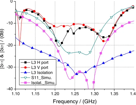
L3 H port L3 V port L3 Isolation S11_Simu. Isolat._Simu.
Figure 8. Measured and simulated L-band element|S11|.
satisfactory, as concluded in Table 4. The measured polarization isolation curve is not so good as the simulated results with value better than 25 dB over the L-band bandwidth.
-90 -60 -30 0 30 60 90 -50 -40 -30 -20 -10 0
Normalized Pattern / (dB)
Angle / (degree)
horizontal / Co-pol vertical / Co-pol horizontal / X-pol vertical / X-pol vertical / Simu. horizontal / Simu.
(a) Horizontal port excited
-90 -60 -30 0 30 60 90
-50 -40 -30 -20 -10 0
Normalized Pattern / (dB)
Angle / (degree)
horizontal / Co-pol vertical / Co-pol horizontal / X-pol vertical / X-pol vertical / Simu. horizontal / Simu.
(b) Vertical port excited
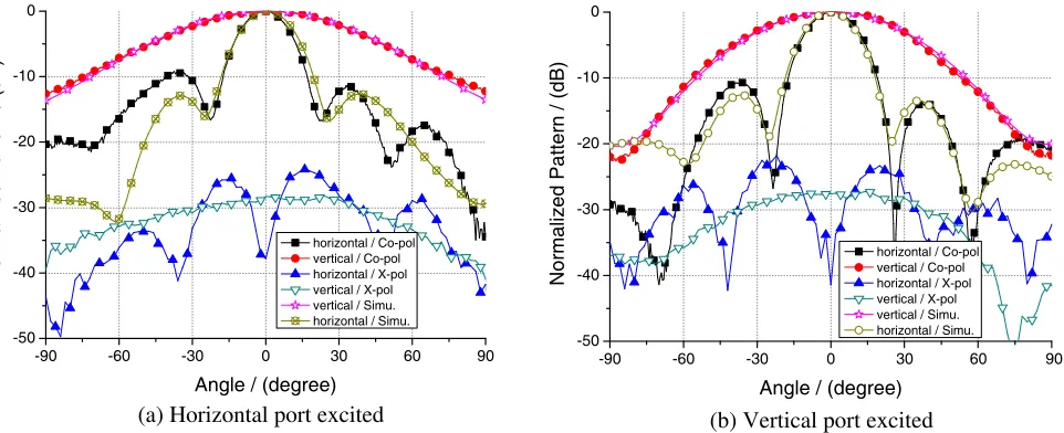
Figure 9. Measured and simulated L-band radiation pattern at 1.25 GHz.
4.8 5.0 5.2 5.4 5.6 5.8 6.0 6.2 -40 -30 -20 -10 0 |S 11
| / (d
B
)
Frequency / (GHz)
Simulated Measured |S11|<-10dB Bandwidth
(a) Return loss
5.0 5.2 5.4 5.6 5.8 6. 0 -40 -38 -36 -34 -32 -30 -28 -26
Isolation / (dB)
Frequency / (GHz)
(b) Isolation between H and V polarizations
Figure 10. Measured and simulated C-band element port response.
Figure 9 presents the measured radiation patterns of uniform excited L-band elements. The patterns agree well with Ansoft HFSS prediction. A deficiency in measured L-band radiation pattern is its left first side-lobe level, which is a bit higher than the theoretical value. This result can mainly attribute to the limited array scale and asymmetric boundary condition, as shown in Fig. 4(a). The radiation patterns are expected to be improved with the extension of the subarray, because boundary condition for L-band array will become more symmetric in this case. The measured cross-polarization level in mainlobe area is roughly 28 dB lower than the co-polarization.
The measured L-band gain is 12.9 dB, corresponding to an efficiency of 86.7%. Due to the limited element number, the scan radiation pattern is not measured.
4.2. C-Band
-90 -60 -30 0 30 60 90 -60 -50 -40 -30 -20 -10 0
Normalized Pattern / (dB)
Angle / (degree)
horizontal / Co-pol horizontal / X-pol horizontal / Array factor
(a) Horizontal port excited patterns in horizontal plane
-90 -60 -30 0 30 60 90
-60 -50 -40 -30 -20 -10 0
Normalized Pattern / (dB
)
Angle / (degree)
vertical / Co-pol vertical / X-pol vertical / Array Factor
(b) Horizontal port excited patterns in vertical plane
-90 -60 -30 0 30 60 90
-60 -50 -40 -30 -20 -10 0
Normalized Pattern / (dB)
Angle / (degree)
horizontal / Co-pol horizontal / X-pol horizontal / Array factor
(c) Vertical port excited patterns in horizontal plane
-90 -60 -30 0 30 60 90
-60 -50 -40 -30 -20 -10 0
Normalized Pattern / (dB)
Angle / (degree)
vertical / Co-pol vertical / X-pol vertical / Array Factor
(d) Vertical port excited patterns in vertical plane
Figure 11. Measured and calculated C-band radiation pattern at 5.8 GHz.
measured array polarization isolation, which refers to the insertion loss between total H- and V-ports, is better than 28 dB in the interested bandwidth, as shown in Fig. 10(b).
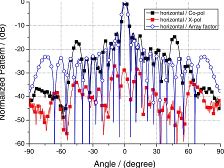
Due to the budget reason, a set of custom-made co-axial lines with different lengths, instead of phase shifter and beam control board, are employed in C-band radiation pattern measurement. Fig. 11 presents the measured radiation patterns of uniform excited C-band array. In general, the measured results agree well with the theoretical array factor. Note that the radiation patterns of vertical plane (defined in Fig. 3(a)) have higher near side-lobe levels and narrower beamwidth than theoretical prediction. This pattern irregularity may come from the limited aperture length and the shielding effect from L-band parasitic patch. The side-lobe level is expected to decrease to the theoretical value with the increasing of aperture length, as evidenced by the patterns of horizontal plane in Fig. 10. In boresight radiation pattern, the measured cross-polarization level is 28 dB lower than the co-polarization in main beam area for both ports.
The C-band calibrated gains ofH- andV-ports are 26.8 dB and 26.6 dB, respectively, corresponding to efficiencies of 81.8% and 78.1%. Note that the loss on coaxial line and power divider is already measured and compensated from array isolation in the data post-process stage. This efficiency is a bit low, where insertion loss of C-band complicated vertical feeding and the raising of near side-lobe are two possible reasons.
-90 -60 -30 0 30 60 90 -40
-30 -20 -10 0
N
o
rmalized Pattern / (dB
)
Angle / (degree)
broadside 7° 14° 21° 28° theory
Figure 12. Simulated C-band scan radiation pattern at 5.8 GHz.
plane is not impacted, as shown in Fig. 3(a) and Fig. 4(a). The scan patterns at 5.8 GHz are measured to verify the scan performance of the proposed structure, as shown in Fig. 12. The antenna gain-dropping rate fits well with the experience equation: G= cos1.5θ, whereθ is the scan angle. From the measured scan pattern, grating lobes are not observed over the scan range, while SLL remains 10 dB lower than main lobe. Scan capability of 25◦ is thus confirmed.
4.3. Result Comparison
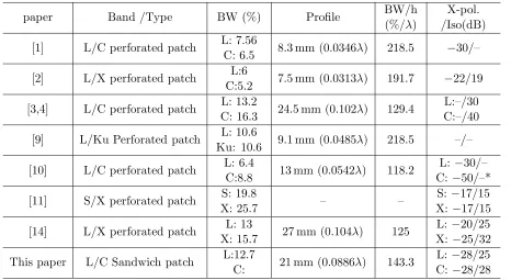
The measured results are concluded and listed in Table 4, with some other published perforated stack patches for comparison.
Table 4. Some published perforated stack patch for DBDP array.
paper Band /Type BW (%) Profile BW/h
(%/λ)
X-pol. /Iso(dB)
[1] L/C perforated patch L: 7.56
C: 6.5 8.3 mm (0.0346λ) 218.5 −30/–
[2] L/X perforated patch L:6
C:5.2 7.5 mm (0.0313λ) 191.7 −22/19
[3,4] L/C perforated patch L: 13.2
C: 16.3 24.5 mm (0.102λ) 129.4
L:–/30 C:–/40
[9] L/Ku Perforated patch L: 10.6
Ku: 10.6 9.1 mm (0.0485λ) 218.5 –/–
[10] L/C perforated patch L: 6.4
C:8.8 13 mm (0.0542λ) 118.2
L:−30/– C: −50/–*
[11] S/X perforated patch S: 19.8
X: 25.7 – –
S:−17/15 X:−17/15
[14] L/X perforated patch L: 13
X: 15.7 27 mm (0.104λ) 125
L:−20/25 X:−25/32
This paper L/C Sandwich patch L:12.7
C: 21 mm (0.0886λ) 143.3
L:−28/25 C: −28/28
From the table, a clear trend can be observed that the antenna profile grows faster than the bandwidth, i.e., the bandwidth-to-profile ratio decreases with the antenna thickness increasing. The perforated stacked patches in [3, 4, 14] have a similar lower band bandwidth to this paper; however, the sandwiched structure in this paper has a lower profile, i.e., the sandwiched structure has a better ‘bandwidth-to-profile’ ratio.
It should be noted that ‘sandwich structure’ still has some limitation at the present stage: 1) It can hardly be used when frequency ratio is large than 4 : 1. In this case, too many higher band elements will be overlapped on the lower band driven patch, which leads to difficulties in designing higher band vertical feeding; 2) The employing of some advanced feeding method, such as aperture coupling, becomes more difficult, although it is still possible [24]. 3) The sandwiched DBDP shared aperture array has a more complex structure, while the bandwidth improvement is not dramatic.
In general, the ‘sandwiched’ DBDP antenna can be employed in some radar system and SAR system due ro its good radiation performance, broad bandwidth and low profile.
5. CONCLUSION
A novel L/C DBDP shared aperture sandwiched stacked patch array is proposed in the paper. For the purpose of improving the lower band bandwidth in DBDP shared aperture array, an L/C-band prototype antenna subarray, including 4×1 elements for L-band and 16×6 elements for C-band, is designed, fabricated and measured. Good bandwidth, radiation performances and scan ability are confirmed, which verifies the feasibility of the design.
ACKNOWLEDGMENT
This work was supported by the Macquarie University iMQRES scholarship scheme and Australian Research Council. The authors would like to thank Mr. Kuang-Da Chen for his great support in antenna measurements and valuable suggestions.
REFERENCES
1. Shafai, L. L., W. A. Chamma, et al., “Dual-band dual-polarized perforated microstrip antennas for SAR applications,” IEEE Trans. Antennas Propagat., Vol. 48, No. 1, 58–66, 2000.
2. Pozar, D. M. and S. D. Targonski, “A shared-aperture dual-band dual-polarized microstrip array,”
IEEE Trans. Antennas Propagat., Vol. 49, No. 2, 150–157, 2001.
3. Wincza, K., S. Gruszczynski, and J. Grzegorz, “Integrated dual-band dual-polarized antenna element for SAR applications,” 2009 IEEE Wirel. Microw. Technol. Conf. (WAMICON’09), 1– 4, Clearwater, Florida, Apr. 2009.
4. Jaworski, G., T. Maleszka, et al., “Dual frequency & dual-linear polarization integrated antenna array for application in synthetic aperture radar,”2010 Europ. Microw. Conf. (EuMC), 1714–1717, Paris, France, Sep. 2010.
5. Shafai, L. and W. Chamma, “Bandwidth and polarization characteristics of perforated patch antennas,”10th Intl. Conf. Antennas Propagat. (ICAP), Vol. 1, 43–46, Edinburgh, UK, Apr. 1997. 6. Hsu, S. H., Y. J. Ren, and K. Chang, “A dual-polarized planar-array antenna for S-band and
X-band airborne applications,”IEEE Trans. Antennas Propagat., Vol. 51, No. 4, 70–78, 2009. 7. Vetharatnam, G., C. B. Kuan, and C. H. Teik, “Combined feed network for a shared-aperture
dual-band dual-polarized array,”IEEE Antennas Wirel. Propagat. Lett., Vol. 4, 297–299, 2005. 8. Vallecchi, A., G. B. Gentili, and M. Calamia, “Dual-band dual polarization microstrip antenna,”
IEEE Antennas Propagat. Society (APS) Intl. Sympo., Vol. 4, 134–137, Columbus, Ohio, Jun. 2003.
9. Schippers, H., J. Verpoorte, P. Jorna, A. Hulzinga, A. Thain, G. Peres, and H. van Gemeren, “Development of dual-frequency airborne satcom antenna with optical beamforming,”2009 IEEE
10. Isleifson, D. and L. Shafai, “A study on the design of dual-band perforated microstrip antennas for SAR applications,” Antenna Technology and Applied Electromagnetics (ANTEM), 1–3, Toulouse, 2012.
11. Lee, Y., D. Ga, et al., “Design of a bandwidth enhanced dual-band dual polarized array antenna,”
Proceedings of ISAP2012, 1281–1284, Nagoya, Japan, 2012.
12. Lee, Y., D. Ga, et al., “A dual band and dual polarization array antenna for AMRFC application,”
Antennas and Propagation Society International Symposium (APSURSI), 1–2, Chicago, IL, 2012.
13. Zhuo, S. G. and T. H. Chio, “Dual-wideband and dual-polarized shared aperture antenna,”
Proceedings of ISAP2012, 798–801, Nagoya, Japan, 2012.
14. Zhuo, S. G. and T. H. Chio, “Dual-wideband, dual-polarized shared aperture antenna with high isolation and low cross polarization,”Proceedings of ISAP2012, 798–801, Nagoya, Japan, 2012. 15. Liu, X., S. He, H. Zhou, J. Xie, and H. Wang, “A novel low-profile dual-band dual-polarization
broadband array antenna for 2G/3G basestation,”2006 IET Intl. Conf. Wirel., Mobile Multimedia
Networks (ICWMMN), 1–4, Hangzhou, China, Nov. 2006.
16. Sun, Z., S. S. Zhong, K. P. Esselle, Y. J. Guo, and Y. Cai, “Broadband dual-band dual-polarized overlapped antenna element,” APWC 2012, 223–226, 2012.
17. Kaboli, M., M. S. Abrishamian, et al., “High isolation dual band dual polarized antenna,” 6’th
International Symposium on Telecommunications (IST’2012), 1–6, 2012.
18. Waterhouse, R. B., “Design of probe-fed stacked patches,” IEEE Trans. Antennas Propagat., Vol. 47, No. 12, 1780–1784, 1999.
19. Granholm, J. and K. Woelders, “Dual polarization stacked microstrip patch antenna array with very low cross-polarization,” IEEE Trans. Antennas Propagat., Vol. 49, No. 10, 1393–1402, 2001. 20. Liang, X.-L., S.-S. Zhong, and W. Wang, “Cross-polarization suppression of dual-polarization linear
microstrip antenna arrays,” Microw. Opti. Tech. Lett., Vol. 42, No. 6, 448–451, 2004.
21. Zaman, A. U., L. Manholm, and A. Derneryd, “Dual polarised microstrip patch antenna with high port isolation,” Electron. Lett., Vol. 43, No. 10, 551–552, May 2007.
22. Zhong, S. S., Z. Sun, L. B. Kong, C. Gao, W. Wang, and M. P. Jin, “Tri-band dual-polarization shared-aperture microstrip array for SAR applications,”IEEE Trans. Antennas Propagat., Vol. 60, No. 9, 4157–4165, 2012.
23. Kona, K. S. and Y. R. Samii, “Novel probe-feeding archetectures for stacked microstrip patch anetennas,”Micro. Opti. Tech. Lett., Vol. 38, No. 6, 467–475, Sep. 2003.