A Compact Single-Element Pattern Reconfigurable Antenna with
Wide-Angle Scanning Tuned by a Single Varactor
Haozhan Tian1, *, Lijun Jiang2, and Tatsuo Itoh1
Abstract—In this paper, we propose a convenient fixed-frequency beam steering method, using a single patch antenna controlled by only one electronically tunable component. The antenna is based on coupled-mode patch antenna (CMPA) [1] that is capable to scan the beam as the function of frequency. A ground-etched slot loaded with one varactor diode is tuned to be capacitive, resonant, or inductive. In order to test broader tuning range, two kinds of varactors with the ranges of 9.24 pF–1.77 pF and 2.67 pF–0.63 pF are implemented respectively. By analyzing how the loaded slot affects the cavity modes and fields, we demonstrate how the voltage bias tunes the frequency responses and steers beam of the antenna. Perturbed by the loaded slot, the frequency response of the antenna shifts from center frequency of 2.35 GHz with the bandwidth of 4.26% down to the band centered at 2.3 GHz with the bandwidth of 4.35%. The maximum scanning range is realized at around 2.29 GHz where the measured main beam continuously scans from −34◦ to +32◦ when the varactor with lower tuning range is used and biased. Meanwhile, the main beam of 2.35 GHz scans from +32◦ to +54◦ when the higher-range varactor is biased. The proposed single-element antenna is able to maintain high gain and efficiency that are comparable to a regular patch antenna with same size and substrate.
1. INTRODUCTION
Beam steerable antennas are drawing more attentions due to the rapid development of wireless communications. These antennas are capable to exploit the spatial dimension of the signal channels by forming the beam toward the desired direction. Along with multiple-input-multiple-output (MIMO) technology, those antennas can mitigate communication impairments, like multipath fading and co-channel interference, and thus improve link quality [2]. Reflector antennas can be used to steer beam by mechanically rotating the reflectors. But they suffer from bulky structures and are typically limited to large mounting platforms. As an alternative, electronically controlled beam-forming arrays [3–6] are widely used in many communication systems. They form the beam by manipulate the phase among multiple radiation elements, which typically results in a bulky size. In addition, it requires complex signal processing and controls to operate, which makes it high cost and limits the application.
Single-element beam forming antennas, also known as pattern reconfigurable antennas, have been developed to provide another solution for beam steering. Leaky wave antenna (LWA), as an example, scans beam as a function of frequency. The energy propagates along the antenna and gradually leaks out. The scanning range can be very wide by applying composite right/left-handed (CRLH) metamaterial structure [7]. To make the beam scan at fixed frequency, many methods have been reported like multi-terminal feeding [8] and integration of tunable components [9], such as p-i-n diodes, microelectromechanical system (MEMS) switches, and varactor diodes. Similar methods have been used in many other designs for beam control [10–13]. However, it could be difficult to integrate multi-terminal
Received 14 February 2019, Accepted 23 April 2019, Scheduled 27 April 2019
* Corresponding author: Haozhan Tian ([email protected]).
feeding antennas with other parts of transmitter, and the designs may not be robust when too many tunable components are applied.
We have reported a new beam steering antenna, so called coupled-mode patch antenna (CMPA) [1]. It realizes large-range beam scanning as a function of frequency in a modified patch antenna. The metal via posts around the center of the antenna split the patch into two coupled half mode cavities. Two eigen-modes exist, that is, even mode where the two radiating slots of the antenna are in phase, and odd mode, where the slots are out of phase. With proper design, the two-pole frequency response is realized where the poles are corresponding to the coupled modes. When the frequency shifts from one pole to another, the phase difference of the two slots changes and thus the antenna scans the beam like a two-element phased array. Since the phases of the slots are controlled by frequency, if tunable components are introduced into CMPA to manipulate the frequency response, beam steering, or pattern diversification, at fixed frequencies is able to be realized just as reported by [14]. There is, however, one significant drawback of the CMPA design: its beam steering can only go from broadside to forward direction. It would be ideal if we could scan the beam in both forward and backward directions.
In this paper, we present a new fixed frequency beam steering CMPA controlled by one varactor diode loading to a slot on the ground. The loaded slot can equivalently become capacitive, resonant, or inductive as the capacitance of the varactor changes. It thus perturbs the cavity modes and field distributions which control the radiation beam in far field. In order to cover the whole tuning range, we mount two varactors with different tuning ranges, 9.24 pF–1.77 pF and 2.67 pF–0.63 pF, respectively at same location on the same antenna in fabrication. The measured and simulated frequency response and the beam steering are demonstrated, which show the objective forward and backward beam scanning through this single-element antenna tuned by a single varactor. In this paper, the forward or backward radiation refer to the radiation whose beam peak is at positive or negative θ region on E plane, respectively. In addition, since the whole matching band is tuned, we show unique beam behaviors controlled by the bias at the other selected frequencies, which could be useful in certain applications as well. Its compactness, simple operation, low cost, and scan effectiveness are highlight features of the newly proposed methodology.
This paper is organized as follows. In Section 2, we first introduce the fundamental operation theory for CMPA briefly, and then analyze the cavity modes of the proposed antenna under different capacitances of the varactor. Section 3 is about the simulation and measurement results for the design. A short discussion is given in Section 4.
2. ANTENNA DESIGN AND OPERATION
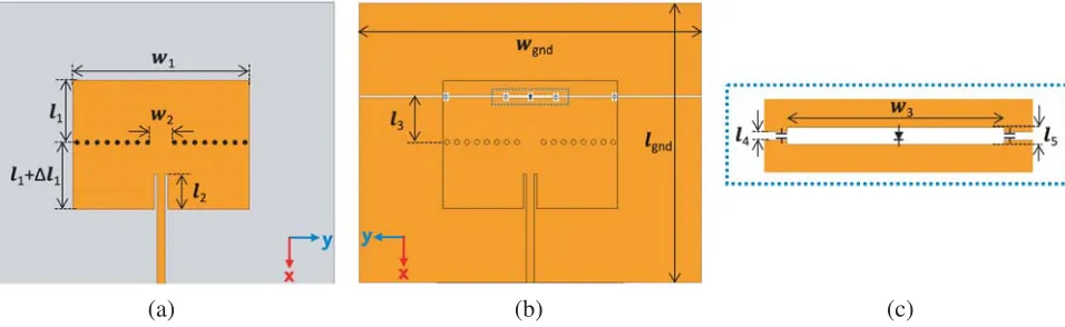
Figure 1 shows the schematic of the proposed antenna. The substrate is a ground-backed Rogers RT/Duroid 5880 substrate with dielectric constant of 2.2, loss tangent of 0.001, and height of 1.575 mm. As shown in Fig. 1(a), the top is an inset-fed rectangular patch with width of w1 = 56 mm and inset
(a) (b) (c)
feeding length of l2 = 11 mm. The metal shorting vias, represented by the black dots, divide the patch into two half-mode cavities with different lengths where l1 = 19.75 mm and Δl1 = 1.5 mm. A coupling gap with width of w2 = 7 mm is opened in the center of the via wall. The ground iswgnd= 110 mm by lgnd= 90 mm as shown in Fig. 1(b). In order to easily apply bias, we etch a slit on the ground that is l3 = 14.75 mm away from the via wall. The width of slit is l4 = 0.6 mm as shown in Fig. 1(c). At the center of the slit, a slot with length of w3 = 15 mm and width of l5 = 1.2 mm is etched like a wider slit and loaded with a varactor diode. Four 10-pF capacitors are installed along the slit where two of them are near the slot, and the other two are under the edges of the top patch. These capacitors compensate the inductive effect of the thin slit on the cavity mode within the operating band and provide the DC block in the same time. On the other hand, the loaded slot does affect the cavity fields. We can then tune the varactor though the bias applied on the ground to control the response of the antenna.
2.1. Fundamental Theory
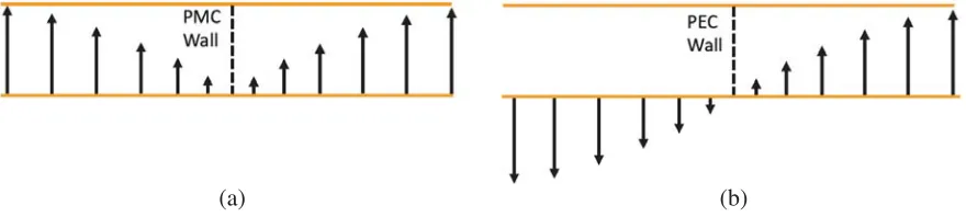
To understand the operation of the antenna, the modes and field distributions in the cavity without the perturbation of the loaded slot are analyzed first. Fig. 2 shows the E field distribution on the xz plane for the two eigenmodes of the coupled cavity. The cavity is simplified to be symmetrically divided where the coupling through a PMC wall leads to the even mode and one through a PEC wall is to the odd mode. The fields at the two sides are in phase at even mode and 180◦ out of phase at odd mode. Two-pole frequency response can be realized when both modes are matched. So when the frequency changes from one pole to the other, the phase changes between 0◦ and 180◦.
(a) (b)
Figure 2. The vector E field distribution in a symmetric coupled cavity at (a) even mode where an equivalent perfect magnetic conductor (PMC) wall is at the center; and (b) odd mode where an equivalent perfect electric conductor (PMC) wall is at the center. The dash line only represents the boundary condition within the coupling gap. The via posts still form a PEC wall in the rest parts.
Since the fringing fields at the edges are equivalent to two magnetic currents that contribute to the far field radiation, the pattern can then be predicted by applying two-element array factor (AF) [15]:
AF = 2 cos
1
2(k0dsinθ+ Δφ)
(1)
where k0 is the propagation constant in free space; d is the separation distance; and Δφ is the phase difference of the two elements. With a fixedd, the main beam scans with the phase difference, which is provided by the coupled modes.
In this design, the varactor loaded slot perturbs the modes and thus affects the frequency response. Since the frequency is corresponding to the phase of the radiating slots as discussed before, we are then able to steer the beam by applying bias voltage. The perturbations of the loaded slot under different capacitances of the varactor are demonstrated in the following subsection. ANSYS High Frequency Structure Simulator HFSSRis used to help with the mode analysis and frequency response. The capacitors and varactor are modeled by applying Lumped RLC Boundary Condition in the simulator.
2.2. Varactor Loaded Slot
A narrow transverse slot on microstrip line is equivalent to a series inductance since it concentrates the magnetic field locally [16]. The inductance value depends on not only the size of the slot but also the location, that is, where the stronger the magnetic field is, the bigger the value can be. Loading the slot with a capacitor can make the whole configuration become capacitive, inductive, or resonant, depending on the equivalent inductance of the slot and the value of the capacitor. Resonant capacitor loaded slot has been reported to be used to generate additional band in a patch antenna [17]. It has to be mentioned that the length of the slot w3 is much smaller than half wavelength, and thus the slot itself is not an effective radiator. The effect of the slot is mainly on the guided fields in the cavity. In our antenna, we carefully design the slot and load it with a varactor to realize both capacitive and inductive response to the cavity within the varactor tuning range.
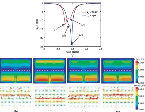
The varactor loaded slot, as part of the upper half mode cavity, affects the resonance of that cavity. Since the slot is serial to the major cavity mode, the resonant frequency of the cavity will be higher when the slot is capacitive than the one when the slot is inductive. On the other hand, the lower half mode cavity is not perturbed by the slot, and the upper and lower cavities will still be coupled through the open iris as long as the resonant frequencies of these two are close. Fig. 3(a) shows the simulated frequency responses of the coupled two cavities when the loaded slot is inductive (Cv = 0.5 pF) and capacitive (Cv = 3 pF). The two-pole response in both cases proves the existence of the coupling. One of the poles overlays for both cases which indicates that the pole is corresponding to the resonance of the lower half mode cavity that is not affected by the slot. While the other pole shifts to high frequency as Cv changes from 0.5 pF to 3 pF, which indicates that the resonant frequency of the upper cavity increases since the loaded slot becomes capacitive.
The lower frequency poles for both cases in Fig. 3(a) are corresponding to even mode. This is determined by the nature of magnetic coupling in the structure. The coupling effect increases the stored flux in each half mode cavity when the magnetic wall is inserted, and it decreases the stored flux when electric wall is in inserted [18]. In consequence, the frequency of even mode is always lower than the one of odd mode in our structure. To prove it, we plot the electric and magnetic field distributions at relevant frequencies with Cv = 0.5 pF andCv = 3 pF in Figs. 3(b)–(e). In both cases, the even and odd modes are excited. Shown in Figs. 3(c) and (e), theE field at the coupling iris is zero, and theH fields of upper and lower cavities point to same direction at odd mode, because of the equivalent PEC wall. The opposite situations appear at even mode, as shown in Figs. 3(b) and (d), due to the PMC wall. Back to Fig. 3(a), the odd mode (higher frequency pole) atCv = 0.5 pF overlays the even mode (lower frequency pole) atCv = 3 pF in certain frequency band. It means that at certain frequency, we are able to change the mode from even to odd by applying proper bias, and thus steer the beam in a wide angle range.
(a)
(b) (c) (d) (e)
(b)
(c)
(d) (e)
Figure 3. (a) Simulated frequency response of the antenna under different capacitances of the varactor Cv. And relevant E and H field distributions in the cavity at (b) low frequency pole 2.301 GHz and (c) high frequency pole 2.363 GHz whenCv = 0.5 pF; at (d) low frequency pole 2.348 GHz and (e) high frequency pole 2.387 GHz when Cv = 3 pF. The varactor is simply modeled by a pure capacitor that is defined by RCL Boundary Condition in HFSS.
Shown in Fig. 4(b) E field distribution where Cv = 2 pF, the fields are concentrated above the slot, while in Fig. 4(c) when Cv = 1.5 pF, the fields are below the slot. This is because the weak coupling between the cavity and slot changes with the loading capacitance.
(a) (b) (c)
(b) (c)
Figure 4. (a) Simulated frequency response perturbed by the slot resonance during the transition from capacitive to inductive. The poles pointed by black arrows are corresponding to the slot resonance, whose E and H field distributions at (b) 2.157 GHz whenCv = 2 pF, and (c) 2.638 GHz whenCv = 1.5 pF are plotted.
3. SIMULATION AND MEASUREMENT
Figure 5 shows the views of the fabricated sample. The bias lines connect on the ground as shown in Figs. 5(a) and (b). Since the bias points are far from the resonant cavity, the high-frequency currents will not drain to the bias lines. In order to cover the whole tuning range, we use two types of plastic packaged varactors from SkyworksR, respectively in our sample, which are SMV1413 ranging from 9.24 pF to 1.77 pF and SMV1405 ranging from 2.76 pF to 0.63 pF. Keysight Advanced Design System (ADSR) and HFSS are used for hybrid simulation in this section to have precise varactor model and get accurate results. In our fabricated sample, the 10-pF capacitors are ATC 500 S Series Surface Mount CapacitorsR, whose self resonant frequency is much higher than the operating frequencies. They can then be treated as ideal capacitors in the simulation. The tuning is in capacitive range while using SMV1413, and it covers all three ranges while using SMV1405.
(a) (b)
(c)
3.1. Performance with Varactor SMV1413
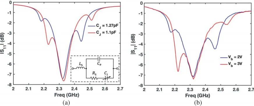
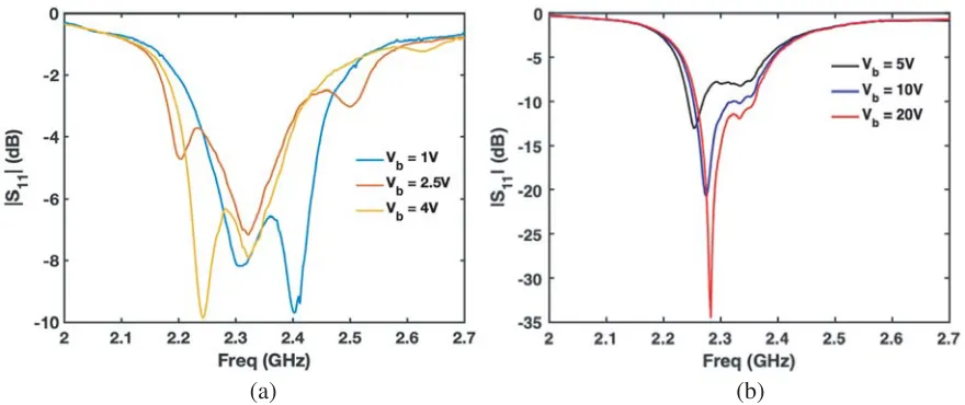
Our antenna is first loaded by Varactor SMV1413 that tunes the slot effective impedance to the cavity in the capacitive range. The simulated frequency responses under different capacitances are shown in Fig. 6(a), where the equivalent circuit model of the varactor is given by the manufacturer. It can be seen that, when the capacitance decreases, the high-frequency pole, corresponding to odd mode, is moving to higher frequency while the low-frequency pole is basically not tuned. This is because the varactor loaded slot only affects the upper cavity, and thus decreasing the capacitance will only increase the frequency of one pole as we discussed before. But it does affect the coupling since the discrepancy of the resonant frequencies for the two cavities becomes larger as the capacitance decreases. As a result, the matching is getting worse. Fig. 6(b) shows the measured frequency responses under different bias voltages on the varactor. As the bias increases, the capacitance of the varactor decreases. Thus in Fig. 6, the measured plots (b) compare closely with the simulated ones (a) under the tolerance of the fabrication. The odd-mode pole shifts from 2.35 GHz to 2.40 GHz as the bias increases from 0 V to 20 V. Meanwhile, the even-mode pole remains at around 2.31 GHz.
(a) (b)
Figure 6. (a) Simulated frequency response under tuning of varactor SMV1413. The inset figure shows the equivalent circuit model of varactor, where the series inductance Ls = 0.7 nH, series resistance Rs = 0.35 Ω, parallel capacitance Cp = 0.3 pF, and junction capacitance CJ is tuned. (b) Measured frequency response under different bias voltages (Vb) for varactor SMV1413.
At any fixed frequency around the high-frequency pole (odd mode), the phase of the radiating slots at backside (upper cavity) is changing as the pole shifting, and thus the beam scans. Fig. 7(a) shows the measured patterns under different bias at 2.35 GHz, which is the frequency of the odd-mode pole forVb = 0 V. As the bias is tuned from 0 V to 20 V, the beam peak continuously scans from 32◦ to 54◦. The measured peak gain and total efficiency versus bias voltage at 2.35 GHz are shown in Fig. 7(b). The peak gain does not take the reflection loss into account, while the total efficiency does. The total efficiency at low bias voltages, where the matching is good, is around 76.5% which is comparable to that of a regular patch antenna with the same size. This indicates that the loss caused by the varactor itself is relatively small. The peak gain decreases from 6.64 dBi to 4.20 dBi as the bias increases from 0 V to 20 V. This is because the mode at 2.35 GHz is odd mode whenVb = 0 V where almost all energy radiates to the main beam direction. But it is getting close to even mode when the bias increases as shown in Fig. 6, which results in an additional side lobe at around θ50◦ in the radiation pattern of Vb = 15,20 V as shown in Fig. 7(a). Thus the energy radiated to the main beam direction decreases. In Fig. 7(b), the total efficiency decreases as the bias voltage increases. The reason is that matching is worse, and the reflection loss increases.
(a) (b)
Figure 7. (a) MeasuredE-plane co-polarized radiation patterns under different bias at 2.35 GHz. The patterns are normalized and plotted in dB scale. (b) Measured peak gain and total efficiency of the antenna versus bias voltage at 2.35 GHz.
0
30
60
90
120
150
180
210 240
270 300
330
-6 -4
-2 0
2 4
V
b = 0 V
Vb = 10 V V
b = 20 V
Figure 8. Measured co-polarized realized gain patterns under different bias at 2.3 GHz onE plane.
pole (even mode), though the pole itself does not shift much with the bias. Shown in Fig. 8 are the patterns for realized gain, which takesS11into account, under different bias at the frequency of 2.3 GHz near the even-mode pole. Since the frequency is around the even mode, there are two beams respectively in positive (forward) and negative (backward)θ regions of the patterns. When biasVb = 0 V, the main beam is pointed at +60◦, and most energy is radiated to the front side. This indicates that the phase of the front radiation slot is initially delayed compared to the one of the back radiation slot, according to the Array Factor in Eq. (1). AsVb increases, the magnitude of the beam on the front side decreases while the one on the back side increases. When bias Vb = 20 V, the peak of the main beam turns to
slot becomes delayed compared to the front one as the bias increases. This pattern behavior makes it possible for the beam of the antenna to scan from backward to forward as the bias changes.
3.2. Wide-Angle Scanning Realized by Varactor SMV1405
We then replace varactor SMV1413 with SMV1405 which has relatively low capacitance tuning range. The tuning ranges of the two varactors have overlays, and thus the slot loaded by SMV1405 is still in capacitive range when the bias is small. In Fig. 9, the measuredS11with SMV1413 under biasVb = 10 V matches well with the one with SMV1405 under bias Vb = 0 V. This indicates that the transition from one varactor to the other is smooth, and the antenna loaded by SMV1405 under small bias will have a similar response to the one discussed in previous subsection.
The varactor loaded slot becomes resonant around the operation frequency when the bias increases, and the capacitance of the varactor further decreases. Simulated and measured frequency responses in the resonant range, shown in Figs. 10(a) and (b) respectively, compare closely. Additional pole that is corresponding to the resonance of the loaded slot comes into the picture and interrupts coupling as we
2 2.1 2.2 2.3 2.4 2.5 2.6 2.7
Freq (GHz) -20
-15 -10 -5 0
|S
11
| (dB)
SMV1413, V b = 10V SMV1405, Vb = 0V
Figure 9. Comparison of the measured frequency response for the antenna loaded by two varactors respectively.
(a) (b)
(a) (b)
Figure 11. Measured frequency response under different bias in (a) the transition (resonant) range and (b) the inductive range.
expected. Though matching is perturbed by the slot resonance, the pole corresponding to the resonance of the lower cavity remains at around 2.32 GHz. This is because the slot does not directly affect the resonance of the lower cavity or the external coupling between the feeding line and the lower cavity. The pole corresponding to the upper cavity shifts from right side to left side of lower cavity pole. As we discussed, the mode at lower cavity pole changes from even to odd mode consequently. When the bias keeps increasing, the additional pole gets to higher frequency, and the loaded slot becomes inductive to the cavity.
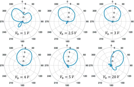
Figure 11 shows the measured frequency response to the bias. The transition from capacitive to inductive region is illustrated in Fig. 11(a), where two-pole response atVb = 1 V first becomes three-pole response due to the slot resonance, and then transfers back to two-pole response with frequency shifting to the left when Vb = 4 V. Fig. 11(b) shows the frequency response in the inductive range. The band of the two-pole response shifts to lower frequency compared to the response in capacitive range. The high-frequency pole, now corresponding to the resonance of the lower cavity, basically remains at same frequency, while the other pole corresponding to the upper cavity shifts to higher frequency as the bias increases, and the loaded slot becomes more inductive. As the resonant frequencies of the two cavities come closer, the coupling becomes stronger, thus the band gets narrower, and matching gets better. From the cavity field perspective, the phase on the back side slot gets delayed more as the bias increases. Consequently, at the frequency around the left-side pole, the radiation beam of the antenna scans with the bias. Meanwhile at around 2.3 GHz, the frequency responses in capacitive, resonant, and inductive ranges overlay, where the maximum beam scanning range can be realized as we discussed in Section 2. Figure 12 shows the measured realized gain patterns of the antenna at 2.29 GHz under different bias. As the bias voltage increases, the main beam of the antenna continuously scans from backward to forward. The beam points to broadside at biasVb = 3 V. The peak of the beam scans from−34◦ to +32◦ as the bias increases from 1 V to 20 V, which results in a total scanning range of 66◦. The realized peak gains under different bias are all above 4 dBi. The whole tuning is realized by only one varactor, SMV1405 model.
Figure 12. Measured co-polarized realized gain patterns onE plane under different bias at 2.29 GHz. The antenna is loaded with varactor SMV1405 only.
0 5 10 15 20
Bias Voltage (V)
3 4 5 6 7 8
Gain (dBi)
0 0.2 0.4 0.6 0.8 1
Efficiency
Figure 13. Measured peak gain and total efficiency of the antenna versus bias voltage at 2.29 GHz.
4. DISCUSSION
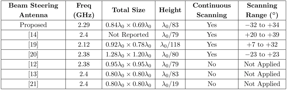
The proposed beam steering antenna has advantages of compact size, simple and low-loss operation, and wide range of continuous beam scanning. In Table 1, we compare the proposed design with other recently reported beam steering antennas or arrays. The antenna in [14] is based on CMPA, similar to the proposed design; it is, however, limited by the beam scanning range. This is because the original CMPA reported in [1] is only capable of beam scanning at the forward region. With the mode perturbed by the loaded slot, the proposed design is able to have much wider scanning range covering both backward and forward regions. Since the proposed antenna is based on a single element patch antenna, the ground and substrate size can be further reduced, even if the total size is already small compared to other designs in Table 1. The single element antennas reported in [12, 13, 21] are compact as well, but they can only achieve certain number of beams instead of continuous scanning, which thus limits their applications. The operation of those designs involves many tuning components and thus is complex. Two-element phased antennas which offer continuous scanning have been reported [19, 20]. Compared with the proposed design, they, however, have larger size and narrower scanning range.
Table 1. Comparison of beam steering antennas.
Beam Steering Antenna
Freq
(GHz) Total Size Height
Continuous Scanning
Scanning Range (◦)
Proposed 2.29 0.84λ0×0.69λ0 λ0/83 Yes −32 to +34
[14] 2.4 Not Reported λ0/79 Yes +20 to +39
[19] 2.12 0.92λ0×0.78λ0 λ0/118 Yes +7 to +32
[20] 2.38 1.28λ0×1.20λ0 λ0/80 Yes −23 to +23
[12] 2.38 0.95λ0×0.95λ0 λ0/79 No Not Applied
[13] 2.4 0.80λ0×0.80λ0 λ0/83 No Not Applied
[21] 2.4 0.80λ0×0.80λ0 λ0/19 No Not Applied
5. CONCLUSION
A single-element beam scanning antenna controlled by only one varactor is presented. The design is based on a coupled-mode patch antenna whose operation is explained by the coupled even and odd modes and two-element array factor. A varactor loaded slot etched on the ground of one of the half-mode cavities is tuned to be capacitive, resonant, or inductive. Two types of varactors, SMV1413 and SMV1405, have been used to cover the whole tuning range. The phases of the radiating slots are then manipulated by applying bias, which leads to both forward and backward beam scanning. Maximum scanning range of 66◦ is achieved at 2.29 GHz where the beam continuously scans from−34◦ to +32◦. The gain and efficiency of this design are comparable to those of a regular patch antenna with same size and substrate.
The design is reliable and robust since all the tuning is simply realized by one component. It has the advantages of compact size, simple and low-loss operation, wide range of continuous beam scanning, low cost, and friendly fabrication. The design can be scaled to different frequency domains. The proposed antenna will find its applications in many 5G communication scenarios, like tracking the mobile platforms from base stations, or tracking the base stations from mobile platforms.
ACKNOWLEDGMENT
REFERENCES
1. Tian, H., K. Dhwaj, L. J. Jiang, and T. Itoh, “Beam scanning realized by coupled modes in a single-patch antenna,” IEEE Antennas and Wireless Propagation Letters, Vol. 17, No. 6, 1077– 1080, 2018.
2. Alexiou, A. and M. Haardt, “Smart antenna technologies for future wireless systems: Trends and challenges,” IEEE Communications Magazine, Vol. 42, No. 9, 90–97, 2004.
3. Nemati, M. H., R. Kazemi, and I. Tekin, “Pattern reconfigurable patch array for 2.4 GHz WLAN systems,”Microwave and Optical Technology Letters, Vol. 56, No. 10, 2377–2381, 2014.
4. Xiao, S., C. Zheng, M. Li, J. Xiong, and B. Z. Wang, “Varactor-loaded pattern reconfigurable array for wide-angle scanning with low gain fluctuation,” IEEE Transactions on Antennas and Propagation, Vol. 63, No. 5, 2364–2369, 2015.
5. Daly, M. P. and J. T. Bernhard, “Beamsteering in pattern reconfigurable arrays using directional modulation,” IEEE Transactions on Antennas and Propagation, Vol. 58, No. 7, 2259–2265, 2010. 6. Ding, X., Y. F. Cheng, W. Shao, H. Li, B. Z. Wang, and D. E. Anagnostou, “A wide-angle scanning
planar phased array with pattern reconfigurable magnetic current element,” IEEE Transactions on Antennas and Propagation, Vol. 65, No. 3, 1434–1439, 2017.
7. Caloz, C., T. Itoh, and A. Rennings, “CRLH metamaterial leaky-wave and resonant antennas,”
IEEE Antennas and Propagation Magazine, Vol. 50, No. 5, 25–39, 2008.
8. Li, Y., Q. Xue, E. K. N. Yung, and Y. Long, “Dual-beam steering microstrip leaky wave antenna with fixed operating frequency,”IEEE Transactions on Antennas and Propagation, Vol. 56, No. 1, 248–252, 2008.
9. Suntives, A. and S. V. Hum, “A fixed-frequency beam-steerable half-mode substrate integrated waveguide leaky-wave antenna,” IEEE Transactions on Antennas and Propagation, Vol. 60, No. 5, 2540–2544, 2012.
10. Christodoulou, C. G., Y. Tawk, S. A. Lane, and S. R. Erwin, “Reconfigurable antennas for wireless and space applications,” Proceedings of the IEEE, Vol. 100, No. 7, 2250–2261, 2012.
11. Bai, Y. Y., S. Xiao, C. Liu, X. Shuai, and B. Z. Wang, “Design of pattern reconfigurable antennas based on a two element dipole array model,” IEEE Transactions on Antennas and Propagation, Vol. 61, No. 9, 4867–4871, 2013.
12. Jusoh, M., T. Aboufoul, T. Sabapathy, A. Alomainy, and M. R. Kamarudin, “Pattern-reconfigurable microstrip patch antenna with multidirectional beam for WiMAX application,”
IEEE Antennas and Wireless Propagation Letters, Vol. 13, 860–863, 2014.
13. Pal, A., A. Mehta, D. Mirshekar-Syahkal, and H. Nakano, “A twelve- beam steering low profile patch antenna with shorting vias for vehicular applications,” IEEE Transactions on Antennas and Propagation, Vol. 65, No. 8, 3905–3912, 2017.
14. Zainarry, S. N. M., S. J. Chen, and C. Fumeaux, “A pattern-reconfigurable single-element microstrip antenna,” 2018 IEEE Radio and Antenna Days of the Indian Ocean (RADIO), 1–2, 2018.
15. Balanis, C. A.,Antenna Theory: Analysis and Design, John Wiley & Sons, 2016.
16. Hoefer, W. J., “Equivalent series inductivity of a narrow transverse slit in microstrip,” IEEE Transactions on Microwave Theory and Techniques, Vol. 25, No. 10, 822–824, 1977.
17. Dhwaj, K., J. M. Kovitz, R. Al-Hadi, and T. Itoh, “Compact dual-band filtering antenna based on capacitor loaded patch radiator,” 2017 IEEE Asia Pacific, Microwave Conference (APMC), 1188–1191, 2017.
18. Hong, J. S. G. and M. J. Lancaster,Microstrip Filters for RF/Microwave Applications, John Wiley & Sons, 2004.
19. Majumdar, B. and K. P. Esselle, “A single band beam scanning active phased array antenna,”
20. Zainarry, S. N. M., N. Nguyen-Trong, and C. Fumeaux, “A frequency- and pattern-reconfigurable two-element array antenna,” IEEE Antennas and Wireless Propagation Letters, Vol. 17, No. 4, 617–620, 2018.