VLSI Architecture for Urdhwa Multiplier
using XOR-XNOR based 4:2 Compressors
1
Ambuj Tiwari, 2Prof. Sonu Lal
1,2
Dept. of ECE, IES College of Technology, Bhopal, India
ABSTRACT: With the advent of new technology in the fields of VLSI and communication, there is also an ever growing demand for high speed processing and low area design. It is also a well-known fact that the multiplier unit forms an integral part of processor design. Due to this regard, high speed multiplier architectures become the need of the day. In this paper, we have developed three designs for Urdhwa Multiplier. In first design we have developed 5:3 compressors based on full adder and utilization in term of 42 delays and 21 areas. In second design we have developed 5:3 compressors based on XOR gate and utilization in term of 36 delays and 24 areas. In third design we have developed 5:3 compressors based on full adder and utilization in term of 28 delays and 18 areas. This all design and experiments were carried out on a Xilinx Vertex-7 series of FPGA and the timing and area of the design, on the same have been calculated.
KEYWORDS: 4:2 Compressor based on Full Adder, 4:2 Compressor based on XOR Gate, 4:2 Compressor based on XOR-XNOR Gate.
I. INTRODUCTION
Digital signal processing (DSP) is the mathematical manipulation of an information signal to modify or improve it in some way. It is characterized by the representation of discrete time, discrete frequency, or other discrete domain signals by a sequence of numbers or symbols and the processing of these signals [1].
The goal of DSP is usually to measure, filter and/or compress continuous real-world analog signals. The first step is usually to convert the signal from an analog to a digital form, by sampling and then digitizing it using an analog-to-digital converter (ADC), which turns the analog signal into a stream of numbers. However, often, the required output signal is another analog output signal, which requires a digital-to-analog converter (DAC). Even if this process is more complex than analogprocessing and has a discrete value range, the application of computational power to digital signal processing allows for many advantages over analog processing in many applications, such as error detection and correction in transmission as well as data compression. DSP algorithms have long been run on standard computers, as well as on specialized processors called digital signal processor and on purpose-built hardware such as application-specific integrated circuit (ASICs). Today there are additional technologies used for digital signal processing including more powerful general purpose microprocessors, field-programmable gate arrays (FPGAs), digital signal controllers (mostly for industrial apps such as motor control), and stream processors, among others [2-3].
II. URDHWA MULTIPLIER
Vedic mathematics is an ancient fast calculation mathematics technique which is taken from historical ancient book of wisdom. Vedic mathematics is an ancient Vedic mathematics which provides the unique technique of mental calculation with the help of simple rules and principles. Swami Bharati Krishna Tirtha (1884-1960), former JagadguruSankaracharya of Puri culled set of 16 Sutras (aphorisms) and 13 Sub - Sutras (corollaries) from the Atharva Veda. He developed methods and techniques for amplifying the principles contained in the formulas and their sub-formulas, and called it Vedic Mathematics. According to him, there has been considerable literature on Mathematics in the Veda-sakhas.
mathematical terms including arithmetic, geometry (plane, co-ordinate), trigonometry, quadratic equations, factorization and even calculus.
4:2Compressor based on Full Adder
To add binary numbers with minimal carry propagation we use compressor adder instead of other adder. Compressor is a digital modern circuit which is used for high speed with minimum gates requires designing technique. This compressor becomes the essential tool for fast multiplication adding technique by keeping an eye on fast processor and lesser area.
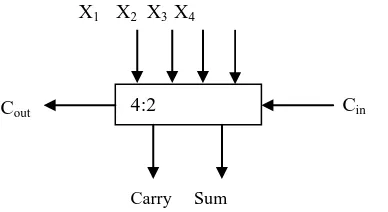
4:2 compressors are capable of adding 4 bits and one carry, in turn producing a 3 bit output. The 5:3 compressors has 4 inputs G1, G2, G3 and G4 and 2 outputs Sum and Carry along with a Carry-in (Cin) and a Carry-out (Cout) as shown in Figure 1. The input Cin is the output from the previous lower significant compressor.
The Cout is the output to the compressor in the next significant stage. The critical path is smaller in comparison with an equivalent circuit to add 5 bits using full adders and half adders. The 5:3 compressors is governed by the basic equation
𝑋1+ 𝑋2+ 𝑋3+ 𝑋4+ 𝐶𝑖𝑛 = 𝑆𝑢𝑚 + 2 ∗ (𝐶𝑎𝑟𝑟𝑦 + 𝐶𝑜𝑢𝑡) (1)
The standard implementation of the 5:3 compressors is done using 2 Full Adder cells as shown in Figure 2.
5:3 Compressor based on XOR Gate
When the individual full Adders are broken into their constituent XOR blocks, it can be observed that the overall delay is equal to 4*XOR. The block diagram in figure 3 shows the existing architecture for the implementation of the 5:3 compressor with a delay of 3*XOR. The equations governing the outputs in the existing architecture are shown below
𝑆𝑢𝑚 = 𝑋1⨁𝑋2⨁𝑋3⨁𝑋4⨁𝐶𝑖𝑛 (2)
Cout
Carry Sum
Cin 4:2
X1 X2 X3 X4
Figure 1: Block Diagram of 5:3 Compressors
Carry Sum
Ci
n
Cout
FA
FA X1 X2 X3X4
𝐶𝑜𝑢𝑡 = 𝑋1⊕ 𝑋2 . 𝑋3+ 𝑋 ∙ 𝑋1+ 𝑋2 3 (3)
𝐶𝑎𝑟𝑟𝑦 = 𝑋1⨁𝑋2⨁𝑋3⨁𝑋4 ∙ 𝐶𝑖𝑛 + (𝑋 ) ∙ 𝑋1⨁𝑋2⨁𝑋3⨁𝑋4 4(4)
Compressor based on XOR Gate
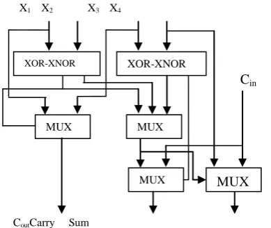
Thus replacing some XOR blocks with multiplexer’s results in a significant improvement in delay. Also the MUX block at the SUM output gets the select bit before the inputs arrive and thus the transistors are already switched by the time they arrive. This minimizes the delay to a considerable extent. This is shown in figure 4.
The equations governing the outputs in the proposed architecture are shown below
𝑆𝑢𝑚 = (𝑋1⨁𝑋2) ∙ (𝑋3⨁𝑋1) ⊺ (𝑋1⨁𝑋2) ∙ (𝑋3⨁𝑋1) ∙ 𝐶𝑖𝑛 (5)
𝐶𝑜𝑢𝑡 = 𝑋1⊕ 𝑋2 . 𝑋3+ 𝑋 ∙ 𝑋1+ 𝑋2 1 (6)
𝐶𝑎𝑟𝑟𝑦 = 𝑋⨁𝑋 ⨁𝑋 ⨁𝑋 ∙ 𝐶 + (𝑋 ) ∙ 𝑋⨁𝑋 ⨁𝑋 ⨁𝑋 (7)
Cin X1 X2 X3 X4
XOR MUX
XOR XOR
XOR MUX
Cout Carry Sum
CoutCarry Sum
Cin
MUX
XOR-XNOR XOR-XNOR
MUX
MUX MUX
X1 X2 X3 X4
7:2Compressor
Similar to its 4:2 compressor counterpart, the 7:2 compressors as shown in figure 5, is capable of adding 7 bits of input and 2 carry’s from the previous stages, at a time.
In our implementation, we have designed a novel 9:4 compressor utilizing two 5:3 compressors, two full adders and one half adders. The architecture for the same has been shown in Figure 6.
2 1
1
S
S
Sum
(8)21 1 3
1
S
C
C
Carry
(9)22 2 3
1
C
C
C
C
out
(10)22 3 2 22 2 3
2
C
C
C
C
C
C
C
out
(11)C
out1C
out2C
in1C
in2X1 X2 X3 X4 X5 X6 X7
Carry Sum 7:2
Figure 5: Block Diagram of 7:2 Compressors
Figure 6: 7:2 Compressor using 4:2 Compressor
C
3C
22C
21S
2C
2C
1S
1F. A. 4:2 Compressor s
4:2 Compressor s
H. A.
F. A.
Cout2 Cout1 Carry1
Sum
1S
III. DELAY AND AREA EVALUATION METHODOLOGY
The delay and area evaluation methodology considers all gates to be made up of AND, OR, and Inverter (AOI), each having delay equal to 1 unit and area equal to 1 unit.
Adder Blocks Delay Area
XOR 3 5
2:1 MUX 3 4
Half Adder 3 6
Full Adder 6 13
We then add up the number of gates in the longest path of a logic block that contributes to the maximum delay. The area evaluation is done by counting the total number of AOI gates required for each logic block.
Architecture No. of Gate
Count
Delay
5:3 Compressor based on Full Adder
42 21
9:4 Compressor 116 57
Compressor based Urdhwa Multiplier
1132 591
5:3 Compressor based on XOR Gate
36 24
Modified 9:4 Compressor
104 63
Modified Compressor based Multiplier
1012 654
5:3 Compressor based on XOR-XNOR Gate
28 18
Proposed 7:3 Compressor
88 51
Proposed
Compressor based
Multiplier
852
531
Table 1: Delay and Area Count of the Basic Blocks of Urdhwa Multiplier
IV. SIMULATION RESULT
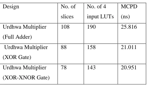
We functionally verified each unit presented in this paper including all three 4:2 Compressor, 7:2 Compressor, Compressor based Urdhwa multiplier. We have been found from the results shown in Table 3 respectively, that number of slices used is same in case of 4:2 compressor based on Full adder and 4:2 compressor based on XOR gate which is less than slices used in 4:2 compressor based on XOR-XNOR gate.
V. CONCLUSION AND FUTURE WORK
Among all three designs, proposed Urdhwa multiplier based on XOR-XNOR gate provides the least amount of Maximum combinational path delay (MCDP). Also, it takes least number of slices i.e. occupy least area among all three design.
REFERENCES
[1] Sushma R. Huddar and SudhirRao, Kalpana M., “Novel High SpeedVedic MathematicsMultiplierusingCompressors ”, 978-1-4673-5090-7/13/$31.00 ©2013 IEEE.
[2] S. S. Kerur, PrakashNarchi, Jayashree C N, Harish M Kittur and Girish V A, “Implementation of Vedic multiplier for Digital Signal Processing”, International Conference on VLSI, Communication & Instrumentation (ICVCI) 2011, Proceedings published by International Joural of Computer Applications® (IJCA), pp.1-6.
[3] HimanshuThapaliyal and M.B Srinivas, “VLSI Implementation of RSA Encryption System Using Ancient Indian Vedic Mathematics”, Center for VLSI and Embedded System Technologies, International Institute of Information Technology Hyderabad, India.
[4] Jagadguru Swami Sri Bharati Krishna Tirthaji Maharaja, “Vedic Mathematics: Sixteen simple Mathematical Formulae from the Veda”, Delhi(2011).
[5] SumitVaidya and DepakDandekar. “Delay-power perfor-mance comparison of multipliers in VLSI circuit design”. International Journal of Computer Networks & Communications (IJCNC), Vol.2, No.4, July 2010.
[6] P. D. Chidgupkar and M. T. Karad, “The Implementation of Vedic Algorithms in Digital Signal Procesing”, Global J. of Eng. Edu, Vol.8, No.2, 204, UICEE Published in Australia.
[7] AsmitaHaveliya, “Design and Simulation of 32-Point FFT Using Radix-2 Algorithm for FPGA Implementation”, Second International Conference on Advanced Computing & Communication Technologies IEEE 2012.
[8] S. Correa, L. C. Freitas, A. Klautau and J. C. W. A. Costa, “VHDL Implementation of a Flexible and Synthesizable FFT Processor”, IEEE LATIN AMERICA TRANSACTIONS, VOL. 10, NO. 1, JAN. 2012.
[9] KamaruAdzha Bin Kadiran. “Design and Implementation of OFDM Transmitter and Receiver on FPGA Hardware”, November 2005.
Design No. of
slices
No. of 4
input LUTs
MCPD
(ns)
Urdhwa Multiplier
(Full Adder)
108 190 25.816
Urdhwa Multiplier
(XOR Gate)
88 158 21.011
Urdhwa Multiplier
(XOR-XNOR Gate)
78 143 20.951