ISSN(Online): 2320-9801
ISSN (Print): 2320-9798
I
nternational
J
ournal of
I
nnovative
R
esearch in
C
omputer
and
C
ommunication
E
ngineering
(An ISO 3297: 2007 Certified Organization)
Vol. 3, Issue 2, February 2015
Implementation on Low Power Design Using
Comparator for VLSI Design Circuit
Uttam Kumar, Ashish Raghuwanshi
M.Tech, Dept. of EC, IES College of Technology, Bhopal, India 1
Assistant Professor, Dept. of EC, IES College of Technology, Bhopal, India2
ABSTRACT: A 8-bit 5GS/s streak simple to-advanced converter (ADC) is composed and reproduced in a 0.18μm
CMOS innovation. Low-swing operation both in the simple and the computerized hardware brings about fast low power operation. The ADC disperses 30mW force from a 3.2V supply while working at 5GHz. Balanced averaging is utilized to minimize the impact of comparator balances. The estimation of greatest differential and indispensable nonlinearities (DNL and INL) of the Flash ADC are 0.2 LSB and 0.5 LSB separately. Simple to-advanced converter (ADC) has ended up fundamental structure for the vast majority of the hardware and correspondence frameworks. Comparator constitutes the fundamental part in simple to computerized transformation (ADC). It is essentially the first stage in ADC, which changes over the sign from simple to computerized space.
KEYWORD: Variable switching voltage, threshold inverter quantization, comparator, Flash ADC
.
I. INTRODUCTION
The Flash ADC is the speediest ADC among a wide range of accessible ADC architectures. A N-Bit Flash ADC utilizes the 2N-1 comparators for information change. Nonetheless, these comparators devour substantial power as they work at the same time in parallel manner. The Streak ADC additionally obliges resistor stepping stool circuit or capacitor exhibit circuit for reference voltage era [2], which again makes the converter more power hungry & subsequently Flash ADC expends most astounding force among a wide range of ADCs. For low power information transformation circuits, the power scattering has turned into a standout amongst the most imperative limits. Actually, control productivity has been considered as a fundamental outline paradigm in numerous battery utilized applications such as remote sensor hub, pacemakers and other embedded RFID chips as biomedical imaging gadgets in the human body [4]. The target in such cases is least power utilization for most extreme battery life time. The outlined 6-Bit Flash ADC in this paper meets the prerequisite for such low power applications.
II. RELATED RESEARCH WORK
ISSN(Online): 2320-9801
ISSN (Print): 2320-9798
I
nternational
J
ournal of
I
nnovative
R
esearch in
C
omputer
and
C
ommunication
E
ngineering
(An ISO 3297: 2007 Certified Organization)
Vol. 3, Issue 2, February 2015
III. COMPARATOR
The capacity of a comparator is to create a yield voltage, which is high or low relying upon whether the sufficiency of the info is more noteworthy or lesser than a reference signal. It delivers a paired yield whose quality is in light of a correlation of two simple inputs. Run of the mill comparators have differential kind of building design, and they can be further partitioned into open-circle and element comparators. The open-circle comparators are in a broad sense operational enhancer [4]. Dynamic comparators use positive input like flip-failures to achieve the correlation of the extent in the middle of data and the outside reference signal. However these differential sorts of comparator are naturally intricate in configuration and expend high measure of force. On the other hand, single finished comparator structural engineering may be conveyed as a simple comparator rather than utilizing an entire simple square of comparator. The edge inverter quantization (TIQ) comparators have been utilized to outline the Flash ADC. The TIQ inverter based comparator comprises of two fell inverters as demonstrated in figure 1. The inverter obliges lesser number of transistors when contrasted with customary comparator. Truth be told, a customary comparator obliges two info sign, while inverter based comparator requires stand out information signal. The rationale reference or exchanging voltage is created by the inverter itself [5]. Graphically, the exchanging voltage can be distinguished at the convergence of the data voltage (Vin) and the yield voltage (Vout) signal. As of right now, both the transistor
PMOS and NMOS are in the immersion district. By likening the channel present of gadgets, the exchanging limit voltage can be dead set. The numerical recipe for these exchanging voltages is given by the emulating mathematical statement [7].
Vsv =( | |) + 1
Figure 1. TIQ Comparator [6]
A. CMOS Design
ISSN(Online): 2320-9801
ISSN (Print): 2320-9798
I
nternational
J
ournal of
I
nnovative
R
esearch in
C
omputer
and
C
ommunication
E
ngineering
(An ISO 3297: 2007 Certified Organization)
Vol. 3, Issue 2, February 2015
B. STATIC CMOS Design
Static CMOS is an outline technique just in combinatorial rationale circuits. A static rationale door is one that has a decently characterized yield once the inputs are balanced out and the exchanging drifters have rotted away. Static CMOS rationale entryways are
moderately simple to outline and utilization. A static CMOS door is a mix of force up system and draw down system as demonstrated in figure 2.
Figure 2 Static Logic style
The capacity of the PUN is to give an association between the yield and VDD at whatever time the yield of the rationale entryway is intended to be 1(based on inputs). So also the capacity of the PDN is to give an association between the yield and GND at whatever time the yield of the rationale entryway is intended to be 0(based on inputs). The PUN and PDN systems are developed in a fundamentally unrelated mold such that unrivaled one system is directing in enduring state. Thusly, once the transient have settled, a way dependably exits in the middle of VDD and the yield or GND and the yield.
IV. VARIABLE SWITCHING VOLTAGE COMPARATOR
ISSN(Online): 2320-9801
ISSN (Print): 2320-9798
I
nternational
J
ournal of
I
nnovative
R
esearch in
C
omputer
and
C
ommunication
E
ngineering
(An ISO 3297: 2007 Certified Organization)
Vol. 3, Issue 2, February 2015
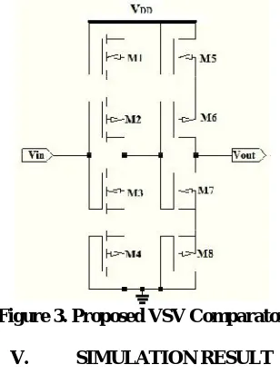
Figure 3. Proposed VSV Comparator
V. SIMULATION RESULT
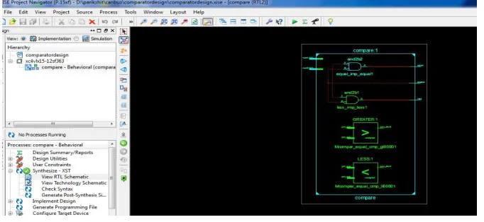
This simulation results shows the TIQ comparator coding done in VHDL on Xilinx software and flash ADC is also on done it with the same software and both simulation results on work through MODELSIM simulator. First simulation shows TIQ comparator result, in this it says about low power is used to produce result. In second one it shows flash 8 bit ADC (analog to digital converter) is used to convert comparator for low power using and producing desired result. Another result shows RTL view of comparator.
ISSN(Online): 2320-9801
ISSN (Print): 2320-9798
I
nternational
J
ournal of
I
nnovative
R
esearch in
C
omputer
and
C
ommunication
E
ngineering
(An ISO 3297: 2007 Certified Organization)
Vol. 3, Issue 2, February 2015
Figure 6 RTL View of Comparator
VI. CONCLUSION
A 8-bit Flash ADC has been outlined by utilizing the proposed VSV comparator. The outline has been done in computerized 65nm standard CMOS innovation. Further lower peculiarity size and littler supply voltage can be consolidated in the outline. At 1 GHz speed, the Flash ADC disseminates top force of 2.1mW and normal force of just
244μW. The measured most extreme differential and vital nonlinearities (DNL and INL) for an incline data are discovered to be 0.3 LSB & 0.6 LSB individually. The parameters DNL & INL are enhanced when contrasted with prior reported works. The planned 6-bit Flash ADC displays noteworthy change as far as power and velocity of already reported Flash ADCs. This makes it very suitable ADC for high speed and low power application.
ACKNOWLEDGMENT
The correspondence author is thankful to all the faculty members of department of Electronics & Communication, IES College of Technology Bhopal, M.P. and India for continuous support and encouragement. This is a prospect to establish our technical skill for the advantage of social civilization.
REFERENCES
[1] Jincheol Yoo, “A TIQ Based CMOS Flash A/D Converter for System on Chip Application”, A Thesis in Computer Sciences and Engineering, .2003
[2] Ali Tangel and Kyusun Choi, “The CMOS Inverter as A Compactor in ADC Design”, Analog Integrated Circuit and Signal Processing, 39 147-155, 2003
[3] S.S. Khot, P.W.Wani, M. S.Sutaone, Shubhang Tripathi “Design Of A 45 M TIQ comparator for High Speed and Low Power 4-Bit Flash ADC”
ACEEE Int. J. On Electrical and Power Engineering Vol.02 No. 01 Feb 2011.
[4] Omar Gonzales, Jonathan Yu, Georgekorbes” 6- Bit Analog to Digital Converter” Dept. of Electrical Engineering, Son Jose State University.
[5] R.Jacob Baker,” CMOS Circuit Design, Layout and Simulation” Second Edition Willey IEEE Press 2004.
[6] Meghana Kulkarni, V.Sridhar, G. H. Kulkarni “The Quantized Differential Comparator in Flash Analog to Digital Converter Design” (IJCNC)
Vol.2, No.4, July 2010.
[7] Deguchi, K., Suwa, N., Ito, M., Kumamoto, T., & Miki, T. (2008) “A 6-bit 3.5-GS/s 0.9-V 98-mW flash ADC in 90-nm CMOS. IEEE Journal of Solid-State Circuits”, Vol. 43, No. 10, pp2303-2310. [8] Kuttner, A. S. T. H. F., Sandner, C., & Clara, M. (2005) “A 6bit, 1.2 gsps low-power flash-adc in 0.13
μm digital cmos”, IEEE Journal of Solid-State Circuits Vol. 40, No.7.
[9] Chen, C. Y., Le, M. Q., & Kim, K. Y. (2009) “A low power 6-bit flash ADC with reference voltage and common-mode calibration”, IEEE Journal of Solid-State Circuits, Vol. 44, No. 4, pp1041-1046.
![Figure 1. TIQ Comparator [6]](https://thumb-us.123doks.com/thumbv2/123dok_us/1493966.1182888/2.595.196.402.414.640/figure-tiq-comparator.webp)