© 2016, IJCSMC All Rights Reserved 38
Available Online atwww.ijcsmc.com
International Journal of Computer Science and Mobile Computing
A Monthly Journal of Computer Science and Information Technology
ISSN 2320–088X
IMPACT FACTOR: 6.017
IJCSMC, Vol. 5, Issue. 12, December 2016, pg.38 – 47
UART Implementation with
BIST Using Verilog-HDL
D Akhila
1, P Mahipal Reddy
21
PG/ VLSI,2Associate Professor, Department of ECE Sree Chaitanya College of Engineering, Karimnagar, Telangana
Abstract:Testing of VLSI chips are becoming very much complex day by day due to increasing exponential advancement of nano technology. So both front-end and back-end engineers are trying to evolve a system with full testability keeping in mind the possibility of reduced product failures and missed market opportunities. BIST is a design technique that allows a system to test automatically itself with slightly larger system size. In this paper, the simulation result performance achieved by BIST enabled UART architecture through VHDL programming is enough to compensate the extra hardware needed in BIST architecture. This technique generate random test pattern automatically, so it can provide less test time compared to an externally applied test pattern and helps to achieve much more productivity at the end.
Keyword: VLSI, BIST, UART, VHDL
I. INTRODUCTION
The processing steps of VLSI chips are extremely complex, and costly inducing vendors to stress on more and more testability as a requirement tool to assure the reliability and the functionality of each of their designed circuits. BIST technique has become as a boon to them, which helps to test a system automatically. Universal Asynchronous Receive/Transmit (UART) has the objectives of firstly to satisfy specified testability requirements, and secondly to generate the lowest-cost with the highest performance implementation. UART has been an important input/output tool for decades and is still widely used. The additional BIST circuit that increases the hardware overhead increases design time and size of the chip, which may degrade the performance [6].This paper focuses on the design of a UART chip with embedded BIST architecture using simple LFSR with the help of VHDL language. The paper describes the problems of (VLSI) testing followed by the behavior of UART that includes both transmitter and receiver section using VHISC Hardware Description Language (VHDL). In this paper, the simulation result is compared with previous work and it has been seen that the result is promising and helps to reduce timing constraints and overall power dissipation. [1]. [2] The UART is targeted at broadband modem, base station, cell phone, and PDA designs.
II. GENERAL BIST ARCHITECTURE
© 2016, IJCSMC All Rights Reserved 39
Circuit under Test (CUT): It is the portion of the circuit tested in BIST mode. It can be sequential, combinational or a memory. It is delimited by their Primary Input (PI) and Primary Output (PO).
Test Pattern Generator (TPG): It generates patterns for the CUT. It is a dedicated circuit or a microprocessor. The patterns may be generated in pseudorandom or deterministically.
Test Response Analysis (TRA): It analyses the value sequence on PO and compares it with the expected output.
BIST Controller Unit (BCU): It controls the test execution; it manages the TPG, TRA and reconfigures the CUT and the multiplexer.
Fig. 1. BIST architecture
Fig. 2. Architecture block diagram
Functionally UART consist of (i) CPU interface and control logic, (ii) Modem control section, (iii) transmitter
section (iv) receiver section.
A. Uart Transmitter Section
© 2016, IJCSMC All Rights Reserved 40
UART transmitter module consists of an output register a transmitter buffer register and transmitter control logic. The i/o pins are:
1. TxD is the port for serial data output
TxC bar is the transmitter clock input 3. TxE is the transmitter control logic output 4. ACK & RST are two control inputs
Fig4: internal architecture of UART transmitter
The PISO block shown in Fig.4, takes 2 input signals: PISO_sel and Reg_load. The 1st one is used to derive a 3rd function of the
block i.e. hold the data bits when the output register is not ready-this is done just by deactivating the clock inside the block. The 2nd one i.e. REG LOAD is high when 8 data bits are loaded parallel in PISO register, i.e. when the output register is ready, the
Counter_3 _bit counts and all the 8 bits are shifted from PISO to Tx_Out register The 3-bit-counter “Counter_3 3bit_SISO” in Tx_Out_reg i.e. The output register of the transmitter module counts 0 to 7 while transmitting the 8 bits serially outside the UART module. When all 8 bits are transmitted the output register is empty and ready to take next 8 bits from PISO register Fig. 5 is the block diagram of the PISO register. This consists of a series of 7 identical block each block contains a D-flip flop and a data transfer logic circuit. There are 2 more flops and one AND gate. So we see that there are effectively 9 D-flip-flops. Dff_2 is the last D-flip-flop which is added to prevent data loss.
Fig. 5. Port Mapping UART transmitter Block
Table1.port name and functionality of UART transmitter
Port Name Port Type Function
DB i/p 8-bit parallel data input to the transmitter
WR i/p A “low” writes the data from the data bus in the transmitter buffer
ACK i/p Acknowledgement signal from the Peripheral (active high).
TxC i/p Transmitter clock signal.
© 2016, IJCSMC All Rights Reserved 41
TxD o/p Serial data output from the transmitter. When no data is transmitted, this remains
“High”.
TxRDY o/p A “high” indicates that the transmitter is ready to transmit data i.e. the transmitter
buffer is empty
TxE o/p A “high” indicates that the transmitter has no data in its output register to transmit
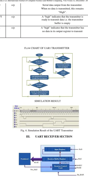
FLOW CHART OF UART TRANSMITTER
SIMULATION RESULT
Fig. 6. Simulation Result of the UART Transmitter
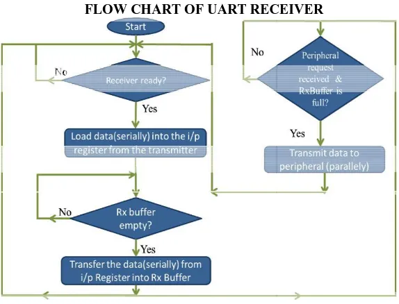
III. UART RECEIVER SECTION
© 2016, IJCSMC All Rights Reserved 42
Fig 7 shows the architecture of UART receiver section. The followings are the brief description of each block.
Input Register:I/P register is a serial input and serial outputregister which consists of 8 D-flip flops to store and shift 8 bit input data. The input data of the register is the serially transmitted data from the transmitter.
Receiver buffer register: It is an 8 bit serial in parallel outregister. The data of i/p register is shifted and enters bit by bit in every rising clock edge in Receiver Buffer Register. After entering 8 bit data, the buffer gets full.
Receiver Control Logic:This block decides when data is tobe taken inside the receiver and when data is to be sent to peripheral device.
Table2: port name and functionality of UART receiver
Port Name Port Type Function
RxD i/p Receiver input data port. It receives the data from the transmitter section
RxC i/p Receiver clock input port. Clock is Fed through this port to the receiver.
PERI- i/p Connected to peripheral device to get RQT The peripheral request input signal.
EN_BAR i/p It is the port in which the receiver Enable signal is fed.
R0-R7 o/p Receiver output data (8 parallel bits) consists a bus
Rx-RDY o/p Connected to transmitter, rxrdy signal Goes out of the port.
Rxfull o/p Connected to transmitter, rx-full Signal goes out of the port.
1) When the peripheral device wants data from the receiver and the receiver buffer register is full simultaneously, then receiver buffer register data are sent to the peripheral device.
2) When the peripheral device does not w ant data from the receiver but the receiver buffer register is full then any data cannot be taken inside the Receiver section and if any data arrives then data should be discarded.
3) When the peripheral device want data from the receiver but the receiver buffer register is not full the n no data is sent to the peripheral and data is taken in Receiver buffer from input register.
4) When the peripheral device does not w ant data from the receiver and the receiver buffer register is not full then data is taken inside Receiver buffer from input register with each clock pulse rising but data is not sent to the peripheral.
© 2016, IJCSMC All Rights Reserved 43
The figure8 is depicting the simulation result of Receiver section. Now, the first eight bits inside the left most donut are seen at the output of receiver after 16 clock cycle delay. After that the next input bits can be seen at the output of the receiver at an interval of 8 clock pulses if, proper signals are there. PERI-RQT is active high sign al. When the signal is high and the receiver buffer is full the receiver buffer data is send to the peripheral device. In the fig the up arrow pointing towards the donut in which the RX FULL signal has gone high as the receiver buffer register become full but at the same time the peripheral device does not want any data, so the receiver is not sending the data towards peripheral at that instance. As the receiver become full so the signal RX RDY (receiver ready) become low, indicating that the receiver cannot take any more data at that instance. So transmitter should n ot send any data towards the receiver. Now the second side arrow pointing towards the 17th input bit ‟0‟ came to the input of the receiver when the receiver is full, so the bit cannot be taken inside the receiver and the 17th bit sent by the transmitter cannot be seen at the output of the receiver.
17TH BIT APPEARING AT O/P
In the figure8 there is an up-arrow pointing towards the donut which is indicating that the RX full and RX RDY both signals are low and high respectively as the peripheral request signal is arrived at the receiver at the same instance when the receiver buffer register become full, so the receiver buffer data is sent to the peripheral at that instance and receiver can keep its normal operation on .So the receiver can take the 17 th bit „0‟ as input (in the previous case which was rejected) inside it at that instance. For that reason we can see the 17 th bit as the input of the receiver (the „0‟ b it) at the output of the receiver (the right most donut indicating that) in the figure8.
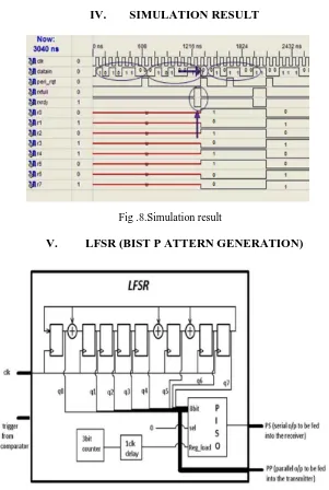
IV. SIMULATION RESULT
Fig .8.Simulation result
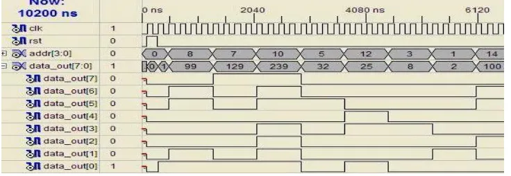
V. LFSR (BIST P ATTERN GENERATION)
© 2016, IJCSMC All Rights Reserved 44
In this figure9 a LFSR of polynomial X8+X6+X 5+1 is made. A PISO with one 3 bit down counter & one 1 CLK delay component is connected. O/P from all DFF comes to the PISO , PISO has another two I/P sel & Reg_load & one PS O/P which serially fed to the receiver.3 bit down counter with 1 CLK delay is connected to the REG LOAD of PISO. Now when SEL is zero O/P from DFF is fed to the receiver serially with every count of the down counter (counter CLK is the trigger signal from comparator). Now when counter value goes to zero i.e 8 bit data has been send to the receiver then PISO will send all 8 bit data parallel to the transmitter in one clock period.
SIMULATION RESULT
The simulation results are presented in the figure 7.2. We can observe that when the trigger signal goes high then only a new value is generated in the LFSR. This LFSR will generate (28-1) different pseudorandom values, and only some of them have been shown in the simulation result. The parallel output “pp” is fed to the transmitter and the serial output is fed to the receiver section of the UART.
Fig. 10. Simulation result of LFSR
ROM:
ROM is used to store the 8-bit pseudo random patterns, in order, that will be obtained as the output from the Transmitter and Receiver sections of the developed UART. The data that are obtained as the outputs of the receiver and the transmitter are compared with the data stored at the corresponding addresses of the ROM by the comparator which verifies whether the CUT is working properly or not.
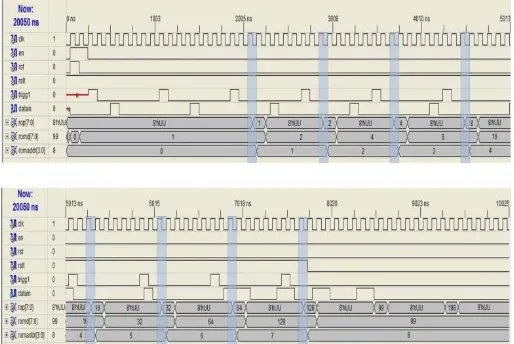
© 2016, IJCSMC All Rights Reserved 45 VI. SIMULATION RESULT OF BIST ENABLED UART
In the figure12 the simulation result of the BIST enabled UART is presented. The overall simulation result of the UART is shown in separate figures. Figure presents the simulation result of the transmitter section and figure13 represents that of the receiver section.
When the trg signal goes high, a new data is obtained from the LFSR which is fed in parallel to the input of the transmitter. After a certain number of clock cycles, the same data is obtained at the output of the transmitter as serial data. This serial data is shifted in the SIPO of the comparator and this is the sipo_op data. This sipo_op is compared with the ROM data (ROMD). The shaded regions in the figure shows the time of comparison. Depending on the comparison, the result (i.e. rslt) is generated. If the both sipo_op and romd are same then rslt=1, else rslt=0.
As the receiver provides 8-bit parallel output, a SIPO is not required in this case. The output from the receiver “rop” is directly compared with romd. The shaded regions in the figure too shows the comparison time. In all the shaded regions, except the last one romd and rop are same and so the rslt is 1 in all those cases. But in the last comparison, due to the intentionally stored incorrect data in the ROM the comparison results in rslt=0. Henceforth comparison procedure is stopped and the CUT is announced to be faulty.
© 2016, IJCSMC All Rights Reserved 46
Figure. 13. Simulation result of BIST enabled UART Receiver
VII. CONCLUSION
This paper implements the VHDL language based coding for BIST technique on UART. UART transmitter and receiver sections are differently tested by BIST technique. The transmitter is given a parallel 8 bit input and the serial output of the transmitter is checked with the respective ideal output stored in the ROM. The receiver is given a serial 8 bit input and the parallel output of the receiver is checked with the respective ideal output stored in the ROM. The checking part is done by comparator section. It compares the receiver or transmitter output with the corresponding data stored in the ROM. Using memory BIST has various advantages such as no external test equipment, reduced development efforts, at-speed tests. However, there are many challenges associated with it such as silicon area overhead, extra pins and routing. In addition, the testability of the test hardware itself is another difficult task. An improvement can be made in the field of implementation of the Test Response Analyzer (TRA). Rather than using ROM as TRA, Multiple Input Shift Register (MISR) can be used for the same purpose. All the simulation result presented in our paper shows that the BIST enabled UART is working well. Hardware test by FPGA Tool (Spartan2E) showed the same result as in the simulation result. The synthesis report that we got from the XILINX tool shows that it provides excellent result compared to the previous work.
Synthesis Report (Design Summary) TIMING Constraints:
Speed Grade: -4
Minimum period: 5.384ns (Max Frequency: 185.736MHz) CPU: 10.80 / 11.06 s | Elapsed: 11.00 / 11.00 s
Total memory usage is 181896 kilobytes Number of errors: 0 (0 filtered)
Number of warnings: 11 (0 filtered) Number of info: 6 (0 filtered)
Clock period: 2.633ns (frequency: 379.795MHz) Total number of paths / destination ports: 6 / 6
A future BIST tester should have very short test time since this ultimately determines the final testing cost. We need high quality test algorithms, those with high coverage which has high correlation to yield. The hardware needs to be simple since this determine the speed and area overhead of the tester. Automatic generation that can ease design efforts will soon demonstrate itself a great value due to the ever increasing time-to-market pressure. The BIST circuit should possess certain degree of self-reparability to improve the fault tolerance and increase reliability. Finally, a flexible BIST that can adapt to engineering and algorithmic changes will greatly reduce system design cost.
REFERENCES
[1] Mohd Yamani Idna Idris, Mashkuri Yaacob, Zaidi Razak, “A VHDL Implementation Of UART Design with BIST capability”
[2] Dr. T.V.S.P. Gupta, Y. Kumari,M.Asok Kumar”UART realization with BIST architecture using VHDL” International Journal
of Engineering Research and Applications (IJERA) ISSN: 2248-9622 www.ijera.com Vol. 3, Issue 1, January -February 2013,
pp.636-640
[3] M.S. Harvey,Generic UART Manual,Silicon Valley,December 1999
© 2016, IJCSMC All Rights Reserved 47
[5] Neil H.E. Weste, Kim Haase, David Harris , A. Banerjee , “CMOS VLSI Design: A circuits and Systems Perspective”,
Pearson Education.
[6] K. Zarrineh, and S. J. Upadhyaya, “On programmable memory built-in self-test architectures”, Design, Automation and Test
in Europe