ABSTRACT
LUO, LEI. Capacitively Coupled Chip-to-Chip Interconnect Design. (under the direction of Dr. Paul D. Franzon)
In modern high performance VLSI chips high-bandwidth and high-throughput are becoming increasingly important. I/O bandwidth in the Multi-Tb/s range is required for current and future high performance VLSI chips. This trend demands high-speed, high-density and low power I/Os.
AC coupled interconnect (ACCI) has been demonstrated as a systematic solution for providing higher pin density, smaller transceiver design and lower power dissipation for high speed chip-to-chip communications. ACCI utilizes non-contact capacitor plates as signal I/O which yields a much higher pin density than traditional solder bump I/O. The coupling capacitors provide passive equalization, thus eliminating the need for costly traditional active equalization. This saves both power and area associated with the equalization circuitry used in a traditional transceiver. ACCI also saves significant power on the transmitter by using pulse signaling instead of traditional non-return-to-zero (NRZ) signaling.
clock and data recovery (CDR), deserializer and bit error rate (BER) tester. ACCI chip-to-chip communication was demonstrated through two 150fF coupling capacitors and a single end terminated 15 cm microstrip line on a FR4 board at 3Gb/s.
C
APACITIVELY
C
OUPLED
C
HIP-
T
O-
C
HIP
I
NTERCONNECT
D
ESIGN
By
L
EI
L
UO
A dissertation submitted to the Graduate Faculty of North Carolina State University
in partial fulfillment of the requirements for the Degree of
Doctor of Philosophy
E
LECTRIAL
E
NGINEERING
Raleigh 2005
APPROVED BY:
_____________________ _____________________
PAUL D FRANZON JOHN M WILSON
Chair of Advisor Committee Co-chair
_____________________ _____________________ _____________________
DEDICATION
BIOGRAPHY
ACKNOWLEDGEMENTS
First of all, I would like to thank Dr. Franzon for offering me this great opportunity to work on the ACCI project. Dr. Franzon always trusted me from the time I joined his group. Without his support, encouragement and referrals, I would not have had the resources to use expensive silicon processes to test my designs and I would not have had the opportunities to work with ARM and Rambus for summer internships, where I further elevated my knowledge and skill. Although he is very busy, Dr. Franzon always has time ready to guide and discuss issues with me. His optimism along with many insights influenced me and drove this project, which were very important and valuable.
I want to thank Dr. Wilson for the many times he provided detailed technical guidance and discussions. Without his help, encouragement and patience, I would not have been able to achieve the results I have today. I also appreciate many late nights Dr. Wilson spent with me in the lab doing measurements. Those exciting moments in the lab will be always be remembered.
I want to thank Dr. Steer, Dr. Davis and Dr. Maria for their knowledgeable and valuable guidance, comments and suggestions to this work. I also learned a lot from the courses taught by Dr. Steer and Dr. Davis.
I learned a lot from my internship experiences with ARM and Rambus. Many skills I learned from them were applied in this thesis. I would like thank Dr. Perkinson, Dr. Gray, Steve, Jason and the others at ARM, and thanks to Fred, Dr. Poulton, Teva, Dr. John Eble, Dr. Palmer, Trey, Jade, Dr. Dettloff and the others at Rambus for all the help and discussions. I also appreciate the discussions and feedback from industry and academia through other channels. This valuable feedback helped us to develop ACCI in a more systematic and detailed manner. I would like thank Dr. Henning and Dr. Banerjee from Intel; Dr. Gerald from AMD, Dr. Bob Evans from Cisco, Dr. Clay Cranford from IBM, Dr. Tom Knight from MIT, and Dr. Angus Kingon from NCSU MSE.
Table of Contents
List of Figures... x
List of Tables ... xv
Chapter 1 Introduction... 1
1.1 Motivation... 1
1.2 Dissertation overview ... 3
1.3 Publications during the Ph.D work ... 4
1.3.1 Journal papers ...4
1.3.2 Conference papers ...5
1.4 Technical Honors Received During the Ph.D Work... 6
1.5 Abbreviations... 6
Chapter 2 Chip-to-Chip Interconnect... 9
2.1 Current commerical high speed links ... 11
2.2 A typical Chip-to-Chip serial link I/O design... 13
2.2.1 Transmitter design ...13
2.2.2 Receiver design...15
2.2.3 Equalization ...16
2.2.4 Timing circuits...22
2.3 Capacitively coupled I/O design... 26
2.3.1 Capacitively coupled chip-to-chip interconnect scheme ...26
2.3.2 Pulse receivers ...29
2.3.3 Other capacitively coupled I/O applications...36
2.3.4 Summary of capacitive coupling I/Os...37
Chapter 3 ACCI Pulse Signaling ... 39
3.1 Introduction... 39
3.2 AC Coupled Interconnect ... 42
3.2.1 Physical Structure ...42
3.2.2 Channel Response...43
3.2.4 Pulse swing ...46
3.3 Pulse Signaling... 48
3.3.1 Pulse Signaling on ACCI...48
3.3.2 Equalization for pulse signaling in ACCI...50
3.3.3 Valid range of coupling capacitor sizes and T-Line Lengths ...52
3.4 Implementation ... 54
3.4.1 Driver design ...54
3.4.2 Voltage Mode Driver...55
3.4.3 Basic Low-Swing Pulse Receiver...57
3.4.4 Low-Swing Pulse Receiver...58
3.4.5 Receiver Input Common-Mode Offset ...61
3.4.6 Receiver Input Noise Margin...62
3.4.7 Simulated Shmoo Plot ...63
3.5 Noise analysis ... 65
3.5.1 Common-mode noise at the receiver input ...65
3.5.2 Power supply noise sensitivity...67
3.6 ACCI design procedure... 69
Chapter 4 Capacitively coupled serial link... 73
4.1 Architecture... 73
4.2 Transmitter path ... 74
4.2.1 Dual loop multi-phase DLL...75
4.2.2 Multiplexer ...80
4.3 Receiver path ... 81
4.3.1 Regenerative sense sampler ...82
4.3.2 Clock phase recovery...86
4.3.3 Pseudo-random bit sequence (PRBS) data generator and BERT...89
4.4 Measurement Results... 90
4.4.1 Test Chip...90
4.4.2 Experimental Results ...91
4.5 Conclusion ... 94
Chapter 5 High Speed ACCI Bus ... 95
5.2 Circuit Implementation ... 97
5.2.1 Differential pulse receiver ...97
5.2.2 Bias Voltage Generator...102
5.3 Signal Integrity on ACCI Bus... 103
5.3.1 Cross talk of ACCI Bus ...103
5.3.2 Switching noise...104
5.4 Test and Measurement ... 107
5.5 Higher speed pulse signaling over ACCI... 110
5.5.1 12.5Gb/s pulse signaling with 90nm CMOS ...111
5.5.2 20Gb/s pulse signaling is expected with 65nm CMOS...114
5.5.3 Summary of technology scaling ...117
Chapter 6 Conclusions... 119
6.1 Conclusions... 119
6.2 Contributions... 121
6.3 Future work... 122
6.3.1 Noise...122
6.3.2 Simple equalization ...124
6.3.3 Clock recovery based on pulse signaling...124
List of Figures
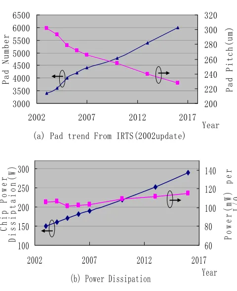
Figure 1.1 Pad and power requirements from IRTS ... 2
Figure 2.1 Off-chip bandwidth Vs On-chip bandwidth ... 9
Figure 2.2 Off-chip Interconnection revolution for medium and long links [8]... 10
Figure 2.3 Traditional current-mode serial link: terminated at both ends to limit reflections; with source coupled current driver and regenerative sense amplifier receiver... 13
Figure 2.4 Traditional serial link transmitter design: MUX, Equalization and driver.... 14
Figure 2.5 Equalization for serial links, can be at either TX side or RX side [17]... 15
Figure 2.6 Traditional serial link receiver design, including sampler and a semi-digital clock and data recovery circuit ... 16
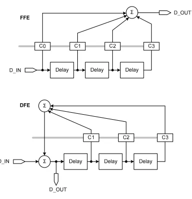
Figure 2.7 (a) FFE and (b) DFE... 17
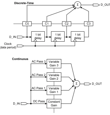
Figure 2.8 (a) Discrete-Time and (b) Continuous Equalization Schemes ... 18
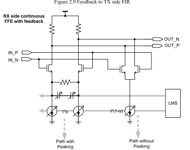
Figure 2.9 Feedback to TX side FIR... 20
Figure 2.10 Feedback to RX side Continuous FFE ... 20
Figure 2.11 decision feedback equalization (DFE)... 21
Figure 2.12 Clock speed: full rate or half rate or quarter rate of serialized data rate ... 23
Figure 2.13 Basic schematic for DLL and PLL loop... 24
Figure 2.14 Semi-digital Dual Delay-locked loop... 25
Figure 2.15 capacitive coupling chip-to-chip interconnect scheme 1: 3D-IC ... 27
Figure 2.16 Capacitively coupled chip-to-chip interconnect scheme 2: Proximity Communication... 28
Figure 2.17 Capacitively coupled chip-to-chip interconnect scheme 3: AC coupled interconnect:... 28
Figure 2.18 AC coupled interconnect with buried solder bumps ... 29
Figure 2.19 Circuit view of capacitive coupling interconnect (a) for 3D-IC and proximity communication in Figure 2.15 and Figure 2.16. (b) for ACCI in Figure 2.17... 29
Figure 2.22 Simplified pulse receiver for proximity communications ... 32
Figure 2.23 Kϋhn’s receiver 2: Comparator with hysteresis ... 32
Figure 2.24 Balanced self-clocked CMOS quantized feedback circuit ... 33
Figure 2.25 Mailland pulse receiver: CM dimmer followed by QF ... 34
Figure 2.26 Knight’s differential pulse receiver ... 35
Figure 2.27 Superconnect pulse receiver: sense amplifier with manually adjusted receiver side clock to achieve low power ... 35
Figure 2.28 Capacitively coupled CMOS(C3MOS) line driver/receiver configuration . 36 Figure 3.1: Comparison with previous CMOS high speed pulse receivers. (All scaled to 0.18µm. To be on the same base line, single ended Vpp is used for single ended pulse receivers in [6][45][67]; differential Vppd is used for differential pulse receivers in [49] and in this work.). ... 41
Figure 3.2: ACCI physical structure (a) top-down view, (b) cross-section view ... 42
Figure 3.3: Channel response of a T-Line channel (solid curve) and an ACCI channel (dotted curve)... 43
Figure 3.4: (a) Transmitter side termination scheme. (b) Impedance looking back from T-Line to coupling capacitor and transmitter... 45
Figure 3.5: Pulse swing depends on edge rate of NRZ signal at driver output... 47
Figure 3.6: Circuit view and transient waveforms of ACCI... 49
Figure 3.7: Frequency domain equalization scheme for pulse signaling in ACCI ... 50
Figure 3.8: Coupling capacitors provide passive high frequency compensation in time domain. The ISI is 3% at the RX input... 51
Figure 3.9: Differential pulse eye diagrams with increasing coupling capacitances... 52
Figure 3.10: Candidates for high speed output drivers: (a) H-bridge with tail current; (b) Current-mode driver; (c) MOS Current-mode Logic (MCML) Inverters [69]; (d) MCML Inverters with feedback to compensate Vth variations [70] ... 54
Figure 3.11: (a) Current-mode driver, (b) voltage mode driver... 55
Figure 3.13: Power savings from voltage mode driver, with a data activity of 0.5, for
6G-10Gb/s data rates, with 90nm CMOS driver ... 56
Figure 3.14: Block view of a basic low-swing pulse receiver with timing/voltage margin ... 57
Figure 3.15: Low-swing, high-speed pulse receiver... 58
Figure 3.16: Jitter at pulses influence the latch operation and lead to jitter at NRZ data ... 59
Figure 3.17: Output clamping for high speed latch operation ... 61
Figure 3.18: RX input offset and deviation ... 62
Figure 3.19: Noise margin of RZ pulse signal at receiver input... 63
Figure 3.20: Simulated shmoo plot with coupling capacitance and T-Line length variations, pass criteria is 0.8UI time opening at the eye diagram of the recovered NRZ data... 64
Figure 3.21: Simulation of common-mode noise on the T-Line and supply noise on transceiver ... 65
Figure 3.22 Surviving Noise margin for all 4 variation corners ... 66
Figure 3.23: Transient simulation with power supply noise model from IBM, with 150fF coupling capacitors and a 20cm T-Line... 68
Figure 3.24: Transient simulations with power supply noise model from IBM, with 90fF coupling capacitors and a 20cm T-Line... 68
Figure 3.25: Basic design flow for capacitively coupled interconnect... 69
Figure 4.1: Block diagram of the test chip... 74
Figure 4.2: Dual-edge controlled Multi-phase DLL ... 76
Figure 4.3: A dynamic phase only detector for multi-phase DLL... 77
Figure 4.4: Charge pump circuit for multi-phase DLL... 78
Figure 4.5: Clock outpt buffer for multi-phase DLL ... 78
Figure 4.6: Overlapped eye diagram of 4-phase clocks, with 15mVpp supply noise... 79
Figure 4.7: Overlapped eye diagram of 4-phase clocks, with 90mVpp supply noise... 79
Figure 4.8: Current steering multiplex based on combinations of multi-phase clocks... 81
Figure 4.10: Timing budget at input of sense sampler... 83
Figure 4.11: Strongarm sense amplifier... 84
Figure 4.12: Measured aperture time on a 60mVpp sense level ... 85
Figure 4.13: Deserialization by 2X oversmapling ... 85
Figure 4.14: 2X oversampling for clock phase recovery... 86
Figure 4.15: Clock phase recovery block diagram ... 88
Figure 4.16: 27-1 Pseudo-Random Bit sequence generator ... 89
Figure 4.17: Bit error judger ... 89
Figure 4.18: Die photo of TSMC 0.18µm CMOS test chip (2mm × 3.5mm) ... 90
Figure 4.19: Test setup on PCB ... 91
Figure 4.20: Measured eye diagram and jitter performance for data and clock ... 93
Figure 5.1: (a) ACCI circuit view and (b) Simulated waveforms... 96
Figure 5.2: INV gain ... 98
Figure 5.3: Fully differential pulse receiver for AC Coupled Interconnect Bus ... 99
Figure 5.4: Common-mode noise margin comparison: complementary pulse receiver versus differential pulse receiver ... 101
Figure 5.5: Adaptive bias voltage generator to track the resistance variation ... 102
Figure 5.6: (a) Power spectrum density of NRZ and RZ pulses, (b) Cross-section view of coupled micro-strip line, (c) Cross Talk Noise of NRZ and RZ-Pulse signal.. 103
Figure 5.7: (a) Voltage mode driver cause switching noise, (b) Reduce switching noise by spreading transition edges, (c) Switching noise largely reduced by spreading I/O edges, according to simulations ... 105
Figure 5.8: Test PCB with 6 pairs of meandered 30cm ACCI channels; the Die photo of CMOS 0.18µm test chip (3.3mm by 3.3mm) ... 107
Figure 5.9: (a) Measured 6Gb/s/Channel RZ-Pulse signal after transmission line (b) Simulated and Measured Shmoo Plot... 108
Figure 5.10: Measured 6Gb/s/Channel Recovered NRZ data (a) transient waveform of a repeated pattern; (b) Recovered Eye diagram of a 27-1 Pseudo-Random Bit Sequence ... 109
Figure 5.12 Simulated Shmoo for 0.75UI opening @ RX OUTPUT @ 12.5Gb/s with
90nm CMOS ... 114
Figure 5.13: Simulation setup for 20Gb/s operation... 115
Figure 5.14: Waveforms for 20Gb/s operation ... 115
Figure 5.15: Eye Diagrams for 20Gb/s operation... 116
List of Tables
Chapter 1 Introduction
1.1
Motivation
(a) Pad trend From IRTS(2002update) 3000 3500 4000 4500 5000 5500 6000 6500
2002 2007 2012 2017 Year Pad Numb er 200 220 240 260 280 300 320 Pad Pitch (um)
(b) Power Dissipation 100
150 200 250 300
2002 2007 2012 2017
Year Chip Power Dissi p taion ( W ) 60 80 100 120 140 Power(mW) per I/O
(a) Pad trend From IRTS(2002update) 3000 3500 4000 4500 5000 5500 6000 6500
2002 2007 2012 2017 Year Pad Numb er 200 220 240 260 280 300 320 Pad Pitch (um)
(b) Power Dissipation 100
150 200 250 300
2002 2007 2012 2017
Year Chip Power Dissi p taion ( W ) 60 80 100 120 140 Power(mW) per I/O
Figure 1.1 Pad and power requirements from IRTS 1
Traditional high speed serial link I/Os use current-mode NRZ signaling. A lot of power is dissipated by the differential current-mode driver. Equalization is necessary to compensate the high frequency loss on the transmission line (T-Line) [3]. Moreover, complicated adaptive equalization is needed to accommodate the variation of high frequency channel loss [4][5].
AC Coupled Interconnect (ACCI) proposed in [6] enables much higher pin density than traditional pin or solder bump technologies. The I/O density that ACCI can provide meets the density requirement predicted by IRTS for year 2017.
ACCI can be applied to high speed serial link applications. Low power, low area and simple implementation can be achieved due to pulse signaling and equalization-free design. This enables even more integration of high speed I/Os [7].
1.2
Dissertation overview
Chapter 2 is a literature review. The trends of serial link design are illustrated and current commercial standards are summarized. A typical serial link transceiver design is described in the architecture level. Applications of previous capacitively coupled I/O designs are reviewed. Both physical structures and circuit designs are discussed.
Pulse signaling with capacitive coupling is proposed in chapter 3 to design low power serial links with passive equalization. Based on the channel response, it is proved that active equalization for high frequency compensation is no longer necessary in ACCI. Instead, a latch based receiver is designed to compensate the low frequency loss. A complementary low swing pulse receiver is designed to allow greater attenuation and to enable smaller coupling capacitors and longer transmission lines (T-Lines). Simulation and analysis on variations of coupling capacitors and T-Line lengths are given.
In chapter 5, a differential pulse receiver is designed for higher bandwidth operation. Signal integrity issues associated with ACCI bus, such as crosstalk, switching noise are analyzed. Higher data rate chip-to-chip communications over ACCI channel with more advanced CMOS technologies are investigated through simulations. Measurements of 36Gb/s operation over 6 bit wide ACCI bus are reported.
In chapter 6, contributions of this work are stated. Future work is proposed as well.
1.3
Publications during the Ph.D work
1.3.1
Journal papers
1. Luo, L.; Wilson, J.; Mick, S.; Xu, J.; Zhang, L. and Franzon, P., “3Gb/s AC Coupled Chip-to-Chip Communication using a Low Swing Pulse Receiver,” to be appeared in Journal of Solid-state circuits, a special issue for ISSCC05, Jan. 2006.
2. Mick, S.; Luo, L.; Wilson, J. and Franzon, P.; “Buried Bump and AC Coupled Interconnection Technology,” IEEE Transactions on Advanced Packaging, vol. 27, pp. 121– 125, Feb. 2004.
1.3.2
Conference papers
1. Luo, L.; Wilson, J.; Mick, S.; Xu, J.; Zhang, L.; and Franzon, P. “A 3Gb/s AC Coupled Chip-to-Chip Communication using a Low Swing Pulse Receiver,” ISSCC Dig. Tech. Papers,
2005,pp. 522-523.
2. Luo, L.; Wilson, J., Xu, J.; Mick, S.; and Franzon, P. "Signal Integrity and Robustness of ACCI packaged systems,” Electric Performance on Electronic Packaging, Oct 2005.
3. Xu, J.; Mick, S.; Wilson, J.; Luo, L; and Franzon, P.; “2.8Gb/s Inductively Coupled Interconnect for 3-D ICs,” in Proc. Symp. VLSI Circuits, 2005.
4. L. Zhang, J. Wilson, R. Bashirullah, L. Luo, J. Xu, and P. Franzon, “Driver Pre-emphasis Techniques for On-Chip Global Buses,” International Symposium on Low Power Electronics and Design, Aug. 2005.
5. Wilson, J., Xu, J.; Mick, S.; Luo, L.; Salvatore Bonafede, Alan Huffman, Richard LaBennett and Franzon, P. " Fully Integrated AC Coupled Interconnect using Buried Bumps,” Electric Performance on Electronic Packaging, Oct. 2005.
6. Xu, J.; Mick, S.; Wilson, J.; Luo, L; Chandrasekar, K.; Enckson, E.; Franzon, P.; "AC Coupled Interconnect for Dense 3-D ICs,” IEEE Nuclear Science Symposium Conference Record, 2003, vol. 1, pp. 125–129.
7. Franzon, P.; Mick, S.; Wilson, J.; Luo, L. and Chandrasakhar K.; Invited Paper, “AC Coupled Interconnect for High-Density High-Bandwidth Packaging” Proc. SPIE,
8. Franzon, P.; Mick, S.; Wilson, J.; Luo, L. and Chandrasekar, K.; “AC Coupled Interconnect for High-Density High-Bandwidth Packaging,” International Conference on Solid State Devices and Materials, Tokyo, Japan, Sep. 2003.
9. Franzon, P.; Kingon, A.; Mick, S.; Wilson, J.; Luo, L.; Chandrasekar, K.; Bonafede, S., Statler; and C., LaBennett, R.; “High Frequency, High Density Interconnect Using AC Coupling,” Materials Research Symposium, Invited Paper, Session B6.1, Boston, Massachusetts, Dec. 2003.
10. Mick, S.; Luo L.; Wilson, J. and Franzon, P.; “Buried solder bump connections for high-density capacitive coupling,” IEEE Electrical Performance of Electronic Packaging, Oct. 2002, pp. 205-208.
1.4
Technical Honors Received During the Ph.D Work
1. Intel Best Student Paper Award at the 14th IEEE Electrical Performance of Electronic Packaging Conference held in Austin, TX, Oct. 2005, for the paper titled "Signal Integrity and Robustness of ACCI Packaged Systems".
2. The ISSCC05 paper “A 3Gb/s AC Coupled Chip-to-Chip Communication using a Low Swing Pulse Receiver” is invited to a Journal of Solid-state Circuit special issue in Jan. 2006. 3. Won 1st place in NC State University ECE Graduate seminar competition, Aug. 2004, Raleigh, NC
1.5
Abbreviations
ACCI AC Coupled Interconnect
BER Bit Error Rate
C3MOS Capacitve Coupled CMOS CDR Clock and Data Recovery CMFB Common-Mode Feed Back DAC Digital to Analog Converter
DLL Delay Locked Loop
DFE Decision Feedback Equalization
FF Flip Flop
FFE Feed Forward Equalization FIR Finite Impulse Response FSM Finite State Machines
PYH Physical layer
IIR Infinite Impulse Response IP Intellectual property
ISI Inter-Symbol-Interference
ITRS International Technology Roadmap of Semiconductor LFSR Linear Feedback Shift Registers
LMS Least Mean Square
LVDS Low Voltage Differential Signaling
MCM Multi-Chip Module
NRZ Non-Return-to-Zero
QF Quantized feedback
PRBS Pseudo-Random Bit Sequence RX Receiver
SNR Signal-to-Noise Ratio
SSN Synchronous Switching Noise T-Line Transmission Line
TX Transmitter TRX Transceiver
VCO Voltage Controlled Oscillators VPPD Voltage Peak-to-Peak Differential
VSEPP Voltage Single-Ended Peak-to-Peak
Xtalk Cross Talk
Chapter 2 Chip-to-Chip Interconnect
For many digital systems, the major performance-limiting factor is the interconnect bandwidth between chips, boards and cabinets. Examples of the applications include Gigabit Ethernet, Xaui, 10GE, Fiber Channel, backplane transceivers, network switches, multi-processor networks and CPU-to-memory links.
0.1 1 10 102 103 104 105 106 107 108
º
º º º
º º º º
º
º
º º º
º º º
º º
1976 1980 1984 1988 1992 1996 2000 2004
8086 '286
'386 '486
P1 P2 P3
P4 (130n)
P4 (90n)
Gates x GHz
Doubles every 16 months
Signal Pins x GHz
Doubles every 28 months
From P2, Signaling rate fraction of processor clock
As VLSI technology continues to scale, system bandwidth will become an even more significant bottleneck. This is because the number of I/Os will scale more slowly than the bandwidth demands of chip logic. Also, off-chip signaling rates have historically scaled more slowly than on-chip clock rates [3], as shown in Figure 2.1.[17]
Figure 2.2 Off-chip Interconnection revolution for medium and long links [8]
transceiver design will then be described at the architecture level. Previous capacitive coupling I/O designs will be presented on both physical structures and circuit levels.
2.1
Current commerical high speed links
Standards Lanes Gb/s Channel coding
Media
1 applications Companies Misc.
SONET
OC-192 1 9.95 FEC O
Data comm. WAN ATT,Verizon, Cisco,Nortel… OC-3-12-48 & OC-768 Infiniband 1,4,8,
12 2.5, 5, 10 8/10 O/E
System/WA N
Intel, Agilent IBM, Sun… Serial RapidIO 1,4 1.25, 2.5,
3.125 8/10 E System
Motorola, Lucent, AD, TI, AMCC… Hyper
Transport
2,4,…
32 Up to 2.8 N/A E
System, chip to chip
AMD,Sun, Apple, Cisco, Broadcom…
Parallel links, share clock per 8 lines, low latency; 10Gb Ethernet 1 10 8/10
64/66 O
Data comm.
LAN 3Com Cisco Intel… Finished on 2002 10Gethernet
XAUI 4 3.125 8/10 E Data comm. 3Com Cisco Intel… Finished on 2002 Fibre Channel 1,4,12 1.06, 2.12,
3.1875, 10.519 8/10 E Storage,
SAN
Agilent, Agere, IBM, Cisco… SAS 1 1.5, 3 8/10 E Storage,
SAN
HP, Intel, LSI logic… PCI Express 1,2,4..
.32 2.5 8/10 E
System, chip to chip
AMD, Cadence, Agilent…
Turbo PCI Express goes to
6Gb/s Aurora 1 to
16 3.125 System, chip Xilinx
RocketIO Up to
20 2.5 to 10 8/10 or 64/66 E Server, SAN Xilinx
Table 2.1 Summary of typical commercial high speed links [54] - [65]
Industry is putting a great deal of effort in designing high speed links, as shown in Table 2.1. Several standards are established. Some of them already have lead to successful products; some of them are at the test stages. Most of these standards are still moving forward to squeeze more bandwidth from the Shannon channel capacitance. Below are some of the trends from this summary table:
1. Most of these high speed links are serial links, which means individual clock and data recovery per line. Hyper Transport is the only exception, where a source synchronous architecture is used and eight channels share one clock. This is used to reduce power and latency for chip to chip applications.
2. Most of the applications employ 8B/10B coding in physical layer. This channel coding is used to balance the number of ‘1’s and ‘0’s, to add activities for clock recovery, to enable error detection and to provide some special characters.
3. No error-correction coding is used in high speed links because the channel response in high frequency region is so bad. The bandwidth penalty due to the error-correction coding overhead will be large especially for high speed links.
4. Most of the optical link designs are at 10Gb/s and are moving forward to 40Gb/s in OC-768. Most of the electrical link designs are at 3Gb/s and are moving forward to 6-10Gb/s in Rocket IO, Turbo PCI Express and Fibre Channel. Electrical cable is cheap and can be high density, but the channel response at high frequency (more than 5GHz) is terrible.
2.2
A typical Chip-to-Chip serial link I/O design
Figure 2.3 shows a traditional current-mode differential serial link [1][3][13][14][15]. A strong transmitter drives differential current over the T-Line. Receiver side termination resistors convert the differential current into voltage swing and feed to one or more sense amplifiers. The clock and data recovery is realized at the receiver side. Data is regenerated by the sense-amplifier based samplers. In the following sections, the architecture and circuit design will be reviewed for transmitter, receiver, timing circuits and equalization schemes.
Figure 2.3 Traditional current-mode serial link: terminated at both ends to limit reflections; with source coupled current driver and regenerative sense amplifier receiver.
2.2.1
Transmitter design
Figure 2.4 Traditional serial link transmitter design: MUX, Equalization and driver
A Multiplexer is necessary to save expensive off-chip I/Os by sharing slow data paths from the logic chip. The shortest achievable clock period in a logic chip in a given technology is limited to be no less than 8τ42 (about 0.8ns in 0.18um technology)[14][16], while the MUX,
driver and the channel can support a much higher data rate with bit period less than τ4. A 4:1
or even 8:1 MUX can be applied to generate a high speed serialized data.
Active equalization is also necessary to extend the data rate and the distances by compensating for the frequency-dependent attenuation of the transmission line mainly due to skin effect and dielectric loss, as shown in Figure 2.5. A digital equalization scheme at the
2τ
transmitter path is proposed in [3]. The analog current summing transmitter FIR filter shown in Figure 2.4 is widely used in serial link designs. Comparing with receiver side equalization, transmitter side equalization is simple to design and implement. But transmitter side equalization is less flexible to channel variation since the tap coefficients are fixed unless adaptive equalization [18][19] is applied.
Figure 2.5 Equalization for serial links, can be at either TX side or RX side [17]
2.2.2
Receiver design
Figure 2.6 shows a typical serial link receiver. The data is 2X over-sampled and then fed into a semi-digital clock and data recovery circuitry. The receiver side equalization can further reduce ISI. Serial link protocols usually set requirements on both the eye opening at transmitter output and the tolerance of eye opening at receiver input. To reach the later requirement, the receiver needs to use equalization to improve the worst required eye opening. Comparing with transmitter side pre-emphasis, receiver side equalization is usually more complex, but offers adaptive equalization capability to meet variations of link and process-voltage-temperature (PVT). Recent designs with adaptive receiver side equalizer are reported in [22][27][28].
Frequency Channel
Bit-ra/e/2
Frequency Equalizing Filter
Bit-ra/e/2
Frequency Equalized Channel
Samplers
Clock Generator
Clocks
Phase Selector and Interpolator Receiver
Equalizer
Digital Control
Logic Data
Figure 2.6 Traditional serial link receiver design, including sampler and a semi-digital clock and data recovery circuit
The sampler is usually implemented by clock triggered regenerative sense amplifier, for example, the strong-arm sense amplifier in [20]. A semi-digital clock and data recovery circuit [21] is widely used because of its unlimited phase capture range crossing variations of data rates and link delays.
2.2.3
Equalization
For a copper trace channel, the high frequency attenuation becomes more severe at higher data rates. Thus, equalization [23]-[26] has become a crucial part of serial link design to reduce inter-symbol-interference (ISI). Both the self-generated noise and noise rejection performance are important when implementing the equalization.
2.2.3.1
Forward and Backward Equalization
Figure 2.7 (a) FFE and (b) DFE
period delay. FFE can be used at either transmitter side as pre-emphasis or at receiver side as high frequency booster.
Figure 2.7 (b) is a decision feedback equalization (DFE). The delay cell here is usually implemented to provide one bit period delay. DFE is usually used at receiver side to remove the ISI. The feedback loop introduces a potential error propagation issue, which is not a problem in FFE.
2.2.3.2
Continuous or Discrete-time Equalization
Equalization can be implemented in either continuous-time or discrete-time. A discrete-time FFE implementation, usually called finite impulse response (FIR) filter, is shown in Figure 2.8 (a). An FIR filter is usually used at the last stage of transmitter to do pre-emphasis or de-emphasis. It can be easily implemented by using digital-analog converter (DAC) tail currents. The side product of pre-emphasis is that it introduces more high frequency signal onto the channel, which could cause more crosstalk noise and switching noise.
A continuous-time implementation, usually called infinite impulse response (IIR) or analog FIR (AFIR) or continuous FFE or “high frequency boost”, is shown in Figure 2.8 (b). It is used at receiver front end to compensate the high frequency loss in the channel. One of the drawbacks of this continuous FFE is that it linearly amplifies both signal and noise at receiver input. The noise comes from crosstalk noise, reflection noise, switching noise, etc.
2.2.3.3
Adaptive Equalization
Figure 2.9 Feedback to TX side FIR
Figure 2.10 Feedback to RX side Continuous FFE
2.2.3.4
Decision Feedback Equalization
peaked at high frequency range, DFE only amplifies the signal. This is because DFE is non-linear and it only feeds back the digitized signal. This feature makes DFE suitable for equalization of a noisy channel.
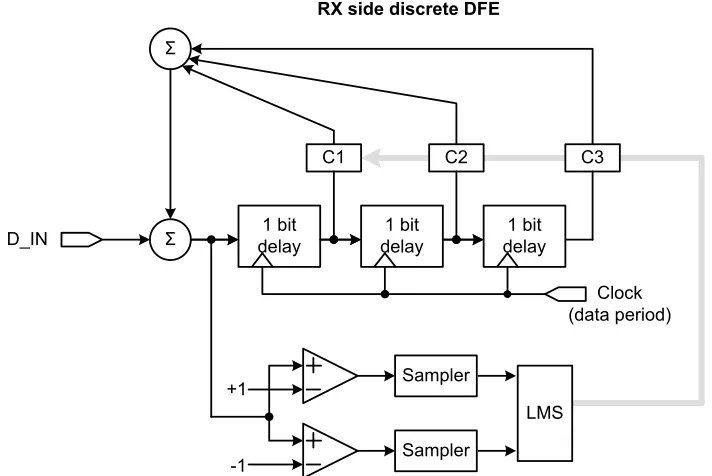
Σ Σ
C1 C2 C3
D_IN delay1 bit delay1 bit delay1 bit
Clock (data period)
Sampler
Sampler
LMS +1
-1
RX side discrete DFE
Figure 2.11 decision feedback equalization (DFE)
However, there are drawbacks in DFE:
1. DFE is usually implemented in discrete-time, which means the clock and data recovery (CDR) needs to perform correctly even before the DFE functions. This requires a preliminary eye diagram opening before DFE functions.
2. DFE has error propagation issue due to its feedback structure, which is not a problem in FFE.
2.2.3.5
Equalization Implementations
Based on the characteristics presented in all these equalization schemes, the most feasible and noise robust serial link would have those three equalization schemes combined together. 1. At transmitter side, use an FIR (discrete FFE) at transmitter side to provide moderate pre-emphasis. Too much transmitter side equalization will cause more noise, such as crosstalk and switching noise.
2. At receiver front end, use an IIR (continuous FFE) to boost high frequency signal and open the signal eye diagram for CDR to operate.
3. Then use a DFE to further reduce ISI and open the eye diagram. DFE is essential to get fine equalization and good BER for noisy channels without amplifying the noise.
2.2.4
Timing circuits
Timing circuits in a serial link include the multi-phase clock generator and the phase recovery circuits.
2.2.4.1
Multi-phase clock generator
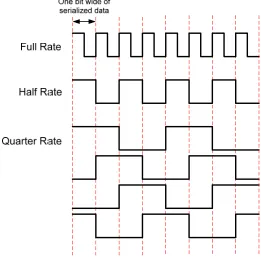
There are three decisions to make when designing the clock generator: 1. Full speed clock versus multiplying clock as shown in Figure 2.12.
bring high frequency noise to its neighbor signal lines. Full rate clocks are usually used in high performance optical transceivers [29][30] where jitter performance is critical.
Figure 2.12 Clock speed: full rate or half rate or quarter rate of serialized data rate
A half rate architecture [31] samples at both the rising and falling edge of the clock. It eases the speed requirement of the VCO, but suffers from the deviation of clock duty cycle.
A multiplying clock can have the same low frequency as the logic clock and they can be shared. It can be quarter rate or even slower. For example, quarter rate clocks [14][15] provide bit period by combination of the four clocks. It eases the clock speed but brings unavoidable deviation of phase offset between neighboring clocks due to uneven matching. Even with a carefully laid out DLL structure, exact quarter phase offset is very difficult to achieve.
PFD & LPF CLK_REF CLK_REF
DLL
PLL
PD & LPF
Figure 2.13 Basic schematic for DLL and PLL loop
2. PLL or DLL
A DLL can only recover clock phase while not frequency. Thus, for the cases where clock synthesis is needed, A PLL is preferred. However, A PLL has a jitter accumulation effect, which makes it more susceptible to power-supply and substrate noise [33]. On the other hand, a DLL is easy to design and is inherently stable. A DLL is used based on the assumption that the capacitively coupled serial link is short and that the TX chip and RX chip can share the same clock source.
3. LC oscillator or ring oscillator
A clock multiplication unit can be implemented as an LC oscillator or a ring oscillator PLL. LC oscillators generate high quality clocks with low power consumption, but the inductor used in this scheme occupies a large area on chip. A ring oscillator PLL occupies moderate area, but the tradeoff between jitter and power results in relatively high power for low jitter generation.[32]
2.2.4.2
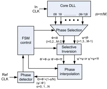
Semi-digital DLL
Phase Selection
Phase interpolation
Selective Inversion
Phase detector FSM control
Ref CLK
In CLK
0θ 1θ ………… (M-1)θ (θ=π/M)
Core DLL
Ф=iθ
(i=0,2...M-2)
ψ=jθ
(j=1,3...M-1)
Ф’=Ф or Ф’=Ф+π ψ’=ψ or ψ’=ψ+π
Θ=Ф’+(1-α/N) (ψ’-Ф’)
α=0, 1...N
Figure 2.14 Semi-digital Dual Delay-locked loop
control unit to generate phase selection and interpolation weight. Phase selection combined with selective inversion covers a seamless 0 to 2π phase range with a phase step of π/M, where M is the multi-phase stages. This π/M phase step is further divided into N stages, which is covered by the phase interpolator, resulting in a final phase step of π/(MN).
2.3
Capacitively coupled I/O design
Capacitive coupling has been used extensively in circuit design. It has been used to isolate different common-mode levels [38][40]; to provide frequency compensation [39], etc.
In chip-to-chip links, capacitive coupling is extensively used in the following three applications:
1. To isolate the common mode voltage difference between transmitter and receiver [37][49][54][55].
2. To reject high range of common mode noise at receiver input [50][51].
3. A high density contact-less AC paths instead of physical solder bumps [41]-[47].
Capacitively coupled interconnects have a number of advantages over conventional conductive interconnects [41]-[44], [53]. The main advantages are high pin density, low power, and passive equalization. Previously reported capacitive coupling interconnect schemes and pulse receivers are reviewed in this section.
2.3.1
Capacitively coupled chip-to-chip interconnect scheme
Chip1
Chip2
Figure 2.15 capacitive coupling chip-to-chip interconnect scheme 1: 3D-IC
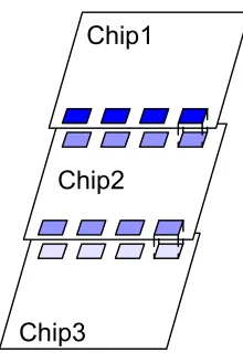
1) Figure 2.15 shows the 3D-IC vertical signal transmission reported in [48] and [45]. Low propagation delay and low power dissipation are achieved by this 3D-IC scheme. In [48], 500MHz data rate is achieved in simulation and 15MHz date rate communication is demonstrated between two vertical chips through a 20um by 20um coupling capacitor (5fF). In [45], a wireless superconnect with a similar physical structure is demonstrated. An 1.27Gb/s/pin and 3mW/pin vertical chip to chip communication is demonstrated through 20um by 20um coupling capacitor. Low power is achieved in design by using a sense amplifier with receiver side clock, as shown in Figure 2.27.
Chip2 Chip1
Chip3
Figure 2.16 Capacitively coupled chip-to-chip interconnect scheme 2: Proximity Communication
3) Multi-chip module (MCM) and ACCI [41][44] are shown in Figure 2.17. In contrast to 3D-IC and proximity communications, the chips in MCM or ACCI don’t communicate with other chips directly. In MCM and ACCI, routing on substrate is available and more chips can communicate with each other. Moreover, the pad distribution on the chip surface can be much more flexible.
Mul ti-la
yer Rou
ting
On Sub
stra te/B
oard
Interconnects
Capacitive Coupling
Trench DC Connection
(Buried Solder Bump)
Chip1 Chip2
Substrate
Figure 2.18 AC coupled interconnect with buried solder bumps
A buried solder bump structure for ACCI is further proposed in [41] and shown in Figure 2.18. The buried solder bumps provide DC paths while the coupling capacitors provide AC paths from chips to substrate. The buried structure enables a smaller gap between the substrate and the chips, which is reverse proportional to the coupling capacitance. The buried solder bumps also provide mechanical support and self-alignment [7].
2.3.2
Pulse receivers
(a)
(b) (a)
(b)
From a circuit view, 3D-IC and proximity communication are structured as shown in Figure 2.19 (a); while MCM and ACCI share the structure shown in Figure 2.19 (b). Scheme b has much more attenuation than scheme a. For scheme b, a termination resistor is needed at either transmitter side or receiver side or both. Transmitters for both schemes are similar, such as an inverter chain to drive NRZ data. After the coupling capacitor, NRZ data is translated into pulse signals shown as Figure 2.20. The receiver needs to recover the pulses back into NRZ data. Since there is much more attenuation in scheme b, the receiver for scheme brequires better input sensitivity than that of scheme a.
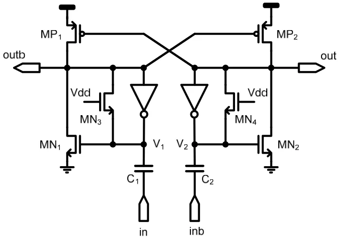
Since the receiver input is isolated by the coupling capacitor, controlling DC wander is one of the challenges faced when designing pulse receivers. Some designs use coding to add data activity to minimize DC wander [37], some circuits can totally remove the DC wander. This section will describe some of the typical pulse receivers reported recently.
2.3.2.1
K
ϋ
hn’s receiver
Kϋhn’s receiver [48] shown in Figure 2.21 is a typical single ended pulse receiver. The first stage is an inverter with diode-connected feedback to bias the local DC voltage to nearly Vdd/2. The second stage is a latch to recover the pulse signal to NRZ data. An inverter isolates two stages and offers some voltage gain. A similar pulse receiver shown in Figure 2.22 is used in proximity communications [46]. This simplified receiver has a similar structure as Kϋhn’s receiver’s latch, but doesn’t have the input bias stage. To address this problem, the feedback inverter output was clamped within a range of VH to VL, which is set
to be about 100mV above and below the switch threshold respectively.
Figure 2.22 Simplified pulse receiver for proximity communications
A comparator with hysteresis [48] is shown in Figure 2.23. MN0, MN1, MN3 and MP0, MP1 are current sources and mirrors. Vin is DC biased at Vref through diode-connected MN6 and
MN7. A positive/negative pulse will decrease/increase Vp , then turned off/on MN2, thus turn
off/on current source MN1, that is decreasing/increasing I1, then decrease/increase Vp, giving
a positive feedback at Vp, so that the output can remain high or low.
Figure 2.23 Kϋhn’s receiver 2: Comparator with hysteresis
2.3.2.2
Quantized feedback (QF) receiver
capacitors, the signals have lost most of their DC components. The two inverters are the positive feedback path, which gives QF to compensate the low frequency insertion loss due to C1 and C2. MN3 and MN4 are clamping devices to make sure the voltage swing between
Vout and V2 remains within a desired range. Cross coupled PMOS (MP1 and MP2) are latch
load, which further latches the detected edge of the signal at V1 and V2. The input pulse
swing requirement is 1Vpp.
Figure 2.24 Balanced self-clocked CMOS quantized feedback circuit
2.3.2.3
Maillard’s pulse receiver
within the good input range of QF circuit. The second stage is a QF circuit similar to [49]. A similar pulse receiver in BiCMOS process [51] presents an 8Gb/s RX with DC input range of
V
690
± and CM edge rejection with up to 4V/ns steepness.
+
P cmc
i
+
N cmc
i
N−cmc
i
−
P cmc
i
Figure 2.25 Mailland pulse receiver: CM dimmer followed by QF
2.3.2.4
Knight’s pulse receiver
Figure 2.26 Knight’s differential pulse receiver
2.3.2.5
Superconnect pulse receiver
Unlike previous pulse receivers, the receiver [45] in Figure 2.27 needs several manually adjusted clocks for the sense amplifier. Vref and Vin are pre-charged to Vdd/2 at ΦPCR and evaluated atΦAMP. The latch load of sense amplifier and the F/F output stage samples the pulse signal and recovered into NRZ data. Power consumption is saved by removing the auto bias circuit and taking advantage of externally adjustable clocks.
2.3.3
Other capacitively coupled I/O applications
A capacitively coupled CMOS (C3MOS) [53] is shown in Figure 2.28. In contrast to previous capacitive coupling I/O, C3MOS has a transmission line but only one coupling capacitor at the transmitter side. The goal of C3MOS is to generate pulse signals using this coupling capacitor to reduce power dissipation on the transmission line. Instead of charging the entire line, small pulses associated with small current packages are launched on the line. The total charge or power dissipation is much smaller than that required to charge the entire line in the traditional NRZ signaling.
2.3.4
Summary of capacitive coupling I/Os
The following is an explanation of different capacitive coupling schemes. 3D-IC and proximity communication use one coupling capacitor to achieve direct chip to chip communication, which has low latency and is applicable for CPU and memory communication. The two overlapped chips need to have exactly the same pad distribution to achieve vertical communication, which is sometimes difficult to achieve. ACCI and MCM have two coupling capacitors and allow routing between dozens of chips. This is applicable for high speed communications among more chips, and pad distribution on the chips are much more flexible. Table 2.2 gives a brief summary of capacitive coupling schemes.
Technique References Objectives Comments Applications 3D-IC [45][48] High density, low latency Limited to two chips memory bus Processor to
Proximity
Communication [46]
High density, low latency
Fixed chip pad distribution, communicates up
to 4 chips
Processor to memory bus,
multi-CPU communication
ACCI on MCM [41][44]
High density I/O with short
range routing
Enables dozens of chips with
flexible pad distribution
multi-CPU communication
C3MOS [53] impulse signals Generate
Reduce power dissipation on
lines
Low power interconnect
Table 2.2 Summary of Capacitively coupled I/O scheme
Pulse RX References Description Comments Kϋhn’s receiver 1 [41][48] a self-biased gain stage and a latch structure High speed
Simple latch [46] Two inverters in a flip-flop configuration
Simple but require careful design on feedback inv to get
proper DC bias Kϋhn’s receiver 2 [48] current switching latch Resistive bias and Lower power without self-bias
Quantized Feedback [49]
A differential scheme using quantized feedback to compensate
DC loss
Low input swing requirement
Maillard’s receiver [50][51]
Current mirrors followed by quantized
feedback
Good Common-mode rejection
Knight’s 4-INV [52]
Four-inverter scheme, two as latch, two as
buffers
Simple and easy match
Clocked sense amp [45]
Pre-charge to bias and evaluate with help of
clock
Low power, need precisely aligned
clocks
Chapter 3 ACCI Pulse Signaling
3.1
Introduction
In contrast to most of the recent results focusing on stacked ICs [45][46][48], the work presented here, ACCI, is optimized for lossy, board-level, capacitively-coupled interconnect. This work enables long distance communication among multiple chips, while retaining the high-density and low-power properties of capacitive coupling. ACCI can not only satisfy the increasing demand for high-density signal I/Os, but also saves precious chip area for more Vdd/Gnd pins to improve power system signal integrity.
In this chapter, the unique band-pass channel response and equalization scheme of the ACCI channel are discussed and compared with traditional low pass response of a T-Line channel. Coupling capacitor and T-Line design rules and design margins are discussed. A voltage mode driver is used for the ACCI channel and saves more than 70% power, when compared to a traditional current-mode driver with conductive signaling. Interconnect power dissipation is minimized by using low swing pulse signaling. For receiver design, previous CMOS single-ended [6][45][67] and differential [49] pulse receivers are reported with more than 200mVpp input swing when scaled to 0.18µm technology, as shown in Figure 3.1. In this
work, a 3Gb/s differential pulse receiver requiring only 120mVpp input swing is proposed.
500 400 300 200 100 0
1 2 3 4 5 6 7 8 This work
Mick CICC02 [4]
Input pu lse s w ing ( m Vpp )
Data rate (Gbps) Pseudo random data Clock signal
Drost JSSC04 [7] Kühn ISCAS95 [5]
Gabara JSSC97 [2] 500 400 300 200 100 0
1 2 3 4 5 6 7 8 This work
Mick CICC02 [4]
Input pu lse s w ing ( m Vpp )
Data rate (Gbps) Pseudo random data Clock signal
Drost JSSC04 [7] Kühn ISCAS95 [5]
Gabara JSSC97 [2]
Figure 3.1: Comparison with previous CMOS high speed pulse receivers. (All scaled to 0.18µm. To be on the same base line, single ended Vpp is used for single ended pulse receivers in [6][45][67];
differential Vppd is used for differential pulse receivers in [49] and in this work.).
Chip-to-chip communication at 3Gb/s is demonstrated through two 150fF coupling capacitors across a 15 cm FR4 microstrip line. On the test chip, the pulse receiver converts pulses into non-return-to-zero (NRZ) data without a clock signal; then a semidigital dual DLL successfully recovers receiver side clock phase from the recovered NRZ data. An on-chip BER tester indicates a BER less than 10-12 through one ACCI channel at 3Gb/s. Given the density made possible by ACCI with this pulse receiver, the ITRS milestone of 110µm pad pitch can be achieved.
3.2
AC Coupled Interconnect
3.2.1
Physical Structure
Substrate Chip1 Chip2 Trench DC Connection (Buried Solder Bump) Interconnects Capacitor Plates Substrate Chip1 Chip2 Trench DC Connection (Buried Solder Bump) Interconnects Capacitor Plates (a) Interconnects Capacitive Coupling Trench DC Connection
(Buried Solder Bump)
Substrate Chip2 Chip1 Interconnects Capacitive Coupling Trench DC Connection
(Buried Solder Bump)
Substrate
Chip2 Chip1
(b)
Figure 3.2: ACCI physical structure (a) top-down view, (b) cross-section view
The buried solder bump has two purposes. First, the solder bumps provide evenly distributed DC connections (e.g. for power, ground and bias signals) across the interface with normal size solder bumps. Second, the buried solder bumps provide a means to self-align the chip and package surfaces while maintaining a close, controlled proximity between corresponding capacitor plates [6]. In this way, evenly distributed AC and DC paths are simultaneously created across the same interface between chip and package (though a MCM is shown, it can be used for conventional packaging). Although capacitive coupling is demonstrated here, inductive coupling is an alternative implementation for ACCI.
3.2.2
Channel Response
R R
R
CC CC
R=50 ohm CC=150fF
50 ohm, 20cm PCB T-Line
4.1g 12.5g 4.1g 12.5g
R R
R
CC CC
R=50 ohm CC=150fF
50 ohm, 20cm PCB T-Line
4.1g 12.5g 4.1g 12.5g
Figure 3.3: Channel response of a T-Line channel (solid curve) and an ACCI channel (dotted curve)
T-Line and parasitic capacitors define the low-pass characteristics while the coupling capacitors define the high-pass characteristics of the ACCI channel response. The series coupling capacitors filter out the low frequency components of transmitted data, thereby, reducing ISI and effectively extend channel bandwidth to higher frequencies. For example, the 3dB bandwidth of the ACCI circuit shown in Figure 3.3 is three times larger (12.5GHz versus 4.1GHz) when compared with a traditional channel having the same T-Line length. However, low frequency attenuation needs to be compensated through equalization and this will be addressed in section 3. It should be noted that there is a need to increase sensitivity of the receivers due to the broad approximate 20dB loss for the ACCI channel compared to the conventional conductive channel.
3.2.3
Impedance match at transmitter side
43.00 45.00 47.00 49.00 51.00
1.E+07 3.E+07 1.E+08 3.E+08 1.E+09 3.E+09 Frequency (Hz) Im pe danc e Z t (o hm ) CC=90fF CC=120fF CC=150fF CC=180fF
(a)
(b)
43.00 45.00 47.00 49.00 51.001.E+07 3.E+07 1.E+08 3.E+08 1.E+09 3.E+09 Frequency (Hz) Im pe danc e Z t (o hm ) CC=90fF CC=120fF CC=150fF CC=180fF
(a)
(b)
Figure 3.4: (a) Transmitter side termination scheme. (b) Impedance looking back from T-Line to coupling capacitor and transmitter
Figure 3.4 (a) shows the termination scheme, where Mp and Mn form the output stage of the
transmitter, CC is the coupling capacitor, CP0 and CP1 are the parasitic capacitance and Rt is
the 50 Ω termination resistor. Figure 3.4 (b) shows Zt, the impedance looking back from
backward wave reflected from receiver side is terminated at the driver side and thus no further reflections are generated. This is proved in the simulation waveforms in Figure 3.6 (b). There is reflection noise at near end T-Line due to the backward reflection at un-terminated far end T-Line. This backward reflection noise is absorbed by the near end termination resistor and thus no further forward reflection noise shown at far end T-Line. The driver output impedance is isolated by the coupling capacitor and thus does not have to be 50 Ω. Zt
is equal to Rt at low frequencies. Though at higher frequencies, the parasitic and coupling
capacitors reduce Zt, the impedance still matches well across a wide range of coupling
capacitor values.
3.2.4
Pulse swing
time and thus longer pulse width, which could bring ISI. Signal4 has the slowest edge rate and thus smallest pulse swing at receiver side.
A
B
C
D
2
1
4
3
2
1
4
3
A
B
C
D
A
B
C
D
2
1
4
3
2
1
4
3
To summarize, the edge rate of the driver output NRZ signal determines the pulse swing while the transition time of the NRZ signal determines the pulse width (neglect the low pass effect of T-Line at this point). Fast edge rate and short NRZ transition time are preferred. This helps to define the best driver for ACCI. Note that infinite edge rate is not preferred due to the switching noise it will cause. So the design trade-off here is among pulse swing, ISI and switching noise.
3.3
Pulse Signaling
3.3.1
Pulse Signaling on ACCI
In contrast to NRZ signaling, pulse signaling has been used to reduce power consumption on interconnect by only dissipating dynamic power [6][53][68]. The band-pass characteristic of the ACCI channel produces return-to-zero pulse signaling, which minimize the power dissipation in the ACCI channel. Figure 3.6 shows the ACCI circuit overview and the transient waveforms at the nodes associated with pulse signaling and pulse receiver.
(b) pulse signaling waveforms (a) circuit view of ACCI
TX Output
Near end T-line
Far end T-line
RX Input
After RX front Inverter
RX Output TX Output
Near end T-line
Far end T-line
RX Input
After RX front Inverter
RX Output
Figure 3.6: Circuit view and transient waveforms of ACCI
scenarios requiring long-range chip-to-chip communication, but it introduces the need for a more sensitive pulse receiver for ACCI.
3.3.2
Equalization for pulse signaling in ACCI
The band-pass characteristic of an ACCI channel uses a different equalization scheme than that used with traditional T-Line channels. High frequency compensation used in traditional T-Line channels is not required in ACCI because the 3dB bandwidth is already extended by three times, as shown in Figure 3.3. However, low frequency compensation is necessary.
ACCI Channel
Frequency Pulse RX (latch)
Bit-rate/2 Frequency Equalized Channel Bit-rate/2 Frequency ACCI Channel Bit-rate/2 Ga in Ga in Ga in ACCI Channel ACCI Channel Frequency Pulse RX (latch)
Bit-rate/2 Frequency Equalized Channel Bit-rate/2 Frequency ACCI Channel Bit-rate/2 Ga in Ga in Ga in Frequency Pulse RX (latch)
Bit-rate/2 Frequency Equalized Channel Bit-rate/2 Frequency ACCI Channel Bit-rate/2 Ga in Ga in Ga in
Figure 3.7: Frequency domain equalization scheme for pulse signaling in ACCI
stable until it detects the next opposite polarity pulse regardless of the bit period, thereby, implementing an adaptive low frequency compensator.
3% Tail
Current Bit Next Bit
13% Tail Time (sec) RX TX Dif fer en tia l pu ls e s w in g ( V ) RZ part Pulse part 3% Tail
Current Bit Next Bit
13% Tail Time (sec) RX TX RX TX Dif fer en tia l pu ls e s w in g ( V ) RZ part Pulse part
Figure 3.8: Coupling capacitors provide passive high frequency compensation in time domain. The ISI is 3% at the RX input.
Figure 3.8 shows, in the time domain, how ACCI extends the bandwidth in the high frequency range. A step input to the channel results in a pulse signal on the T-Line, and at the receiver input. The T-Line has a low-pass response due to the skin effect and dielectric loss, resulting in a long tail on the pulse signal. Without equalization, this tail would cause inter-symbol-interference (ISI) and reduce the timing margin at the receiver. The second coupling capacitor de-emphasizes the low frequency components by filtering the long pulse tail, thereby, reducing energy that interferes with adjacent pulses. This inherent passive behavior allows ACCI to save chip area and power dissipation typically associated with active high frequency compensation.
3.3.3
Valid range of coupling capacitor sizes and T-Line Lengths
The coupling capacitors and T-Line parameters define the ACCI channel response and thus the pulse swing and width at the receiver. For a given data rate and pulse receiver input sensitivity, there are a range of coupling capacitor sizes and T-Line lengths, within which a pulse receiver is able to recover the NRZ data.
Increasing Coupling Capacitance Vpp (mV) Time (ps) 150 100 50 0 -50 -100 -150 -200
0 200 400
ISI limit Swing limit Increasing Coupling Capacitance Vpp (mV) Time (ps) 150 100 50 0 -50 -100 -150 -200
0 200 400
ISI limit
Swing limit
Figure 3.9 shows the differential pulse eye diagram after the second coupling capacitance (i.e. at the input of the receiver). The arrows show the trend resulting from increasing the coupling capacitor size. Larger coupling capacitors will increase the peak-to-peak pulse swing and overall pulse duration. The increased swing relaxes the constraint on the receiver input sensitivity, but the increased pulse width may introduce ISI. The use of a smaller coupling capacitance provides more efficient filtering of the pulse signal tail and reduces ISI, but the corresponding reduction in signal swing increases the input sensitivity requirement for the pulse receiver. Therefore, the maximum coupling capacitance is constrained by the ISI limit, or the data period limit; while the minimum coupling capacitance is constrained by the swing limit, or pulse receiver input sensitivity. (This simple explanation ignores noise in the system. A discussion of noise related issues is covered in a later section.)
Similarly, the T-Line also affects channel response and pulse shape. Longer T-Lines result in more attenuation, especially high frequency attenuation. This not only extends pulse width (increasing ISI) but also limits pulse swing. Thus, the maximum T-Line length is constrained by both the ISI limit and swing limit.
3.4
Implementation
3.4.1
Driver design
(c)
(a)
(d)
(b)
(c)
(a)
(d)
(b)
Figure 3.10: Candidates for high speed output drivers: (a) H-bridge with tail current; (b) Current-mode driver; (c) MOS Current-Current-mode Logic (MCML) Inverters [69]; (d) MCML Inverters with
feedback to compensate Vth variations [70]
power dissipation. The ACCI channel has high input impedance and making it more appropriate to use a voltage mode driver.
3.4.2
Voltage Mode Driver
Itail
(a) (b) Itail
(a) (b)
Figure 3.11: (a) Current-mode driver, (b) voltage mode driver
0 5 10 15 20 25 30 35
0.1 0.2 0.3 0.4 0.5 0.6 0.7 0.8 0.9
Output Swing (Vppd)
P owe r o f Dr iv er ( m W )
Current Mode Driver VM driver at 5Gb/s VM driver at 4Gb/s VM Driver at 3Gb/s VM Driver at 2Gb/s VM Driver at 1Gb/s 70% less 90% less 0 5 10 15 20 25 30 35
0.1 0.2 0.3 0.4 0.5 0.6 0.7 0.8 0.9
Output Swing (Vppd)
P owe r o f Dr iv er ( m W )
Current Mode Driver VM driver at 5Gb/s VM driver at 4Gb/s VM Driver at 3Gb/s VM Driver at 2Gb/s VM Driver at 1Gb/s 70% less
90% less
Figure 3.12: Power savings from voltage mode driver, with a data activity of 0.5, for 1G-5Gb/s data rates, with 0.18um CMOS driver
0 2 4 6 8 10 12 14 16
0.2 0.3 0.4
Output Sw ing (Vppd)
P o we r o f Dr iv e r ( m W )
Current Mode Driver VM Driver at 10Gbps VM Driver at 8Gbps VM Driver at 6Gbps
74% less
85% less
Figure 3.13: Power savings from voltage mode driver, with a data activity of 0.5, for 6G-10Gb/s data rates, with 90nm CMOS driver
depending on data rate. Figure 3.13 shows similar power savings for higher data rates with a 90nm CMOS driver.
Above all, we use complementary inverters for their fast edge rates, low dynamic power dissipation, simple design and smaller circuit area. The disadvantage of the inverter is that dynamic supply current will introduce synchronous switching noise (SSN). This SSN could be reduced by adding slew rate control for low data rate communications and adequate power supply filtering/decoupling. Techniques to reduce this SSN will be discussed in chapter 5.
3.4.3
Basic Low-Swing Pulse Receiver
Bias Amp Pulse to
NRZ 60 ~ 200 mVpp
0.8UI
300 ~ 700 mVpp 0.7UI
600 ~ 800 mVpp 0.6UI
To regenerative sense Amp
Figure 3.14: Block view of a basic low-swing pulse receiver with timing/voltage margin
Figure 3.14 shows the basic functional blocks of the low-swing complementary pulse receiver, with voltage and timing margin noted at each node. In ACCI, since the coupling capacitors block the DC signal, the RX needs to self-bias, then amplify and convert the pulse signals into NRZ data.
To accommodate combinations of coupling capacitors’ size, gap, overlap, tilting and T-Line length, the input sensitivity range is set to be from 60 to 200mVpp. A sense amplifier is
needed to increase pulse swing to be more than 300mVpp, which is the minimum input swing
data, which is ready to be sampled by the regenerative sense amplifier. A 600mVpp swing is chosen with tradeoffs among voltage margin, latch bandwidth and timing margin.
Minimum timing margin at output is set as 0.6UI to insure correct clock recovery operation and good jitter performance in the recovered clock. Input timing margin is set to 0.8UI, considering 0.1UI jitter loss at the transmitter output and another 0.1UI loss on T-Line. The deterministic jitter from ISI is not included since the coupling capacitors provide passive equalization. The “Bias”, “Amplifier” and “Edge Detector” will consume the remaining timing margin up to 0.2UI.
3.4.4
Low-Swing Pulse Receiver
Stage1: Auto-bias & Amplify
Vb
Vpulse IN+
Vnrz OUT+ Vnrz
OUT-Vpulse IN-M1 M3 M5 M2 M4 M6
M7 M8
M11 M12
M10
M9
RXAMP+
RXAMP-Stage2: Latch
Stage1: Auto-bias & Amplify
Vb
Vpulse IN+
Vnrz OUT+ Vnrz
OUT-Vpulse IN-M1 M3 M5 M2 M4 M6
M7 M8
M11 M12
M10
M9
RXAMP+
RXAMP-Stage2: Latch
Figure 3.15: Low-swing, high-speed pulse receiver