DEVASTHALI, VINAYAK SUDHAKAR. Application of Body Biasing and Supply Volt-age Scaling Techniques for LeakVolt-age Reduction and Performance Improvement of CMOS Circuits. (Under the direction of Professor Paul Franzon).
The efficiency of body biasing technique is evaluated in 90-nm process technology
for regular and low threshold voltage devices. A new leakage monitor circuit for detecting
an optimum reverse body bias voltage is designed. The simulation results shows that the
monitor circuit accurately tracks the leakage currents within ±5% of the actual leakage
current values. The standby leakage reduction in static CMOS circuits using reverse body
biasing is presented. The results indicate that the reverse body biasing is more beneficial for
high speed circuits using low threshold voltage devices. For circuits using nominal threshold
voltage devices, the efficiency of reverse body biasing decreases due to the presence of gate
leakage. Speed improvement in ring oscillator and ripple carry adder using forward body
bias is measured. The results show that the forward body biasing is less effective due to the
lower body effect parameter. Supply voltage scaling technique for active power reduction
is implemented using 180-nm technology. Power savings up to 50% is achieved by scaling
by
Vinayak Sudhakar Devasthali
A thesis submitted to the Graduate Faculty of North Carolina State University
in partial fulfillment of the requirements for the Degree of
Master of Science
Electrical and Computer Engineering
Raleigh, North Carolina
2007
Approved By:
Dr. W. Rhett Davis Dr. Kevin Gard
Biography
Vinayak Devasthali was born on July 26, 1983 in Maharashtra, India. He obtained his
bachelor’s degree in Instrumentation Engineering at Vivekananda Education Society’s
In-stitute of Technology, an affiliate of the University of Mumbai, in June, 2004. Since August
2005, he has been a master’s student, majoring in Electrical Engineering, at North Carolina
State University, Raleigh, USA. After graduation, he plans to join Qimonda as a DRAM
Acknowledgments
I would like to take this opportunity to thank the people, who have directly or
indirectly helped me in completing my thesis work.
To start with, I thank my family for supporting me throughout my academic
career. Their faith has helped me to stay positive during tough times.
I am grateful to Dr. Paul Franzon for agreeing to be my thesis advisor. It has
been a privilege to work under his guidance. I highly appreciate his advice and support
when most needed. I thank my thesis committee members, Dr. Kevin Gard and Dr. W.
Rhett Davis, for their valuable comments and suggestions regarding my thesis. They have
been extremely patient with me during the thesis work.
A special round of thanks goes to Shep Pitts and Shrivatsan Parthasarathy for the
enlightening technical discussions. It was in these discussions that I found the seeds of my
thesis topic. I am thankful to Steve Lipa for providing me a workplace and for being tolerant
of me. I would like to thank Dr. H Joel Trussell for offering me a teaching assistantship,
which provided a huge financial relief and helped me concentrate on my thesis work. I also
thank the entire staff of ECE department for their help throughout my graduate studies at
NCSU. In particular, I acknowledge Elaine Hardin’s help in completing the thesis paperwork
and Kaye Bailey’s assistance in arranging a conference room for my thesis defense.
I would also like to thank Jean Appleman and Michael Kleiner of Qimonda for
their understanding and support during the completion of this work.
Finally, I express my sincere gratitude towards my friends at NCSU for all that
I have learnt during my stay in Raleigh. They have been a huge support to me for the
last two years. A special thanks to Manish Sachdev for providing me the LaTeX template
for this thesis, to Saurabh Gupta and Jingzhen Hu for teaching me swimming and driving
respectively, to Po-Chih Lin for numerous rides and to Ajit Gopalakrishnan for an infinite
number of reasons. These people constitute a major motivating force for me in
accomplish-ing whatever I could. I thank them all from the bottom of my heart for the memories that
Contents
List of Figures vi
List of Tables viii
1 Introduction 1
1.1 Motivation . . . 1
1.2 Process Requirements . . . 2
1.3 Research Goal . . . 2
1.4 Thesis Organization . . . 3
2 Leakage Mechanisms in CMOS circuits 5 2.1 Subthreshold Leakage . . . 5
2.1.1 Threshold Voltage Dependence of The Subthreshold Current . . . . 7
2.1.2 Stack Effect . . . 8
2.2 Gate Leakage . . . 9
2.2.1 Input Sequence Dependence of Gate Leakage Current . . . 11
2.2.2 Interdependence of Subthreshold Current and Gate Leakage . . . 12
2.3 Junction Band-to-Band Tunneling (BTBT) Leakage . . . 14
2.4 Leakage Reduction Techniques . . . 16
2.4.1 Design-Time Techniques . . . 16
2.4.2 Run-Time Techniques . . . 17
3 Body Biasing 20 3.1 The Threshold Voltage . . . 21
3.1.1 Body Effect . . . 22
3.2 Short Channel Effects . . . 23
3.2.1 VT H Roll-Off . . . 24
3.2.2 Drain Induced Barrier Lowering (DIBL) . . . 24
3.3 Effect of Body Biasing on Leakage Components . . . 25
3.4 Optimum Reverse Body Bias for Minimum Standby Leakage . . . 27
3.4.1 Previously Designed Leakage Comparator Circuits . . . 27
3.5 Standby Leakage Reduction using Reverse Body Bias . . . 33
3.5.1 Leakage Reduction in Stacked Transistors Configurations . . . 36
3.6 Dynamic Performance Improvement Using Forward Body Bias . . . 37
4 Supply Voltage Scaling 40 4.1 Buck Converter . . . 42
4.1.1 Circuit Operation . . . 43
4.1.2 Analysis of Buck Converter . . . 45
4.1.3 Modes of Operation of Buck Converter . . . 46
4.2 Pulse Width Modulation Technique . . . 48
4.3 Feedback Control Loop Design . . . 48
4.3.1 Phase Frequency Detector(PFD) . . . 50
4.3.2 Charge Pump . . . 54
4.3.3 Loop Filter . . . 54
4.3.4 Ring Oscillator . . . 56
4.3.5 Replica-Feedback Bias Generator . . . 60
4.3.6 Pulse Width Modulator Design . . . 62
4.4 Buck Converter Design . . . 64
4.4.1 Output Low Pass Filter Design . . . 64
4.4.2 Gate Driver Design . . . 65
4.5 Simulation Results . . . 65
4.5.1 Converter Efficiency Calculation . . . 65
4.5.2 Power Savings using Supply Voltage Scaling . . . 68
4.5.3 Power and Area Trade Off . . . 70
5 Conclusion 72 5.1 Contribution of This Work . . . 73
5.2 Future Work . . . 74
List of Figures
1.1 Triple-well Structure . . . 3
2.1 Different Leakage Paths in CMOS Circuits . . . 6
2.2 ID vs VGS plot(logarithmic scale) for NMOS (W = 5µm,L= 80nm,VT H = 245.2mV) in 90-nm process . . . 6
2.3 Threshold Voltage Dependence of Subthreshold Leakage. The drain current of NMOS transistor (W = 5µm, L = 80nm) in 90-nm process against the gate-to-source voltage on a logarithmic scale . . . 8
2.4 Schematic of 2-input NAND Gate . . . 8
2.5 Gate Leakage Tunneling Mechanisms . . . 10
2.6 Stacked NMOS transistors in NAND3 Gate . . . 11
2.7 Band-to-Band Tunneling across a reverse-biased p-n junction . . . 15
2.8 Classification of Leakage Reduction Techniques . . . 16
3.1 Cross-sectional view of NMOS showing depletion region and inversion layer formed below the gate . . . 22
3.2 Variations in leakage components of a NMOS transistor with body bias in 90-nm technology . . . 26
3.3 Leakage Monitor Circuit from [Neau03] . . . 28
3.4 Leakage Monitor Circuit from [Nomura06] . . . 30
3.5 Proposed Leakage Monitor Circuit . . . 31
3.6 Amplifier used in Leakage Monitor Circuit . . . 32
3.7 Leakage Monitor Results . . . 33
3.8 NMOS Off State Leakage Current . . . 35
3.9 PMOS Off State Leakage Current . . . 35
3.10 Total Leakage Current of an Inverter Pair . . . 35
3.11 Increase in on-state current of NMOS device with forward body bias . . . . 38
3.12 Increase in on-state current of PMOS with forward body bias . . . 38
4.1 Buck Converter . . . 42
4.2 Buck Converter Equivalent Circuit During ON State . . . 43
4.4 Current and Voltage Waveforms for the Buck Converter . . . 44
4.5 Inductor Current and Voltage waveforms for CCM and DCM . . . 47
4.6 PWM Control Signal for Switches in Buck Converter . . . 49
4.7 Control-Loop Block Diagram . . . 49
4.8 Phase Frequency Detector Schematic . . . 50
4.9 Timing Waveforms for PFD. V CO CLK < REF CLK . . . 51
4.10 Timing Waveforms for PFD.V CO CLK =REF CLK . . . 52
4.11 Timing Waveforms for PFD.V CO CLK > REF CLK . . . 53
4.12 Charge Pump Schematic . . . 55
4.13 Charge Pump Output Voltage Waveforms . . . 55
4.14 Second Order Loop Filter . . . 56
4.15 Schematic of Differential Delay Cell Used in Ring Oscillator Design . . . 57
4.16 Schematic of 4-stage Ring Oscillator . . . 59
4.17 Ring Oscillator Frequency as a function of Bias VoltageVBP . . . 59
4.18 Schematic of Differential-to-Single-Ended Converter . . . 60
4.19 Replica-Feedback Bias Generator . . . 61
4.20 Start-up Circuit for Replica-Feedback Bias Generator . . . 62
4.21 Schematic of the 2-stage amplifier used in PWM Comparator . . . 63
4.22 Comparator Frequency Response . . . 63
4.23 Output Voltage of Buck Converter for 100MHz operation . . . 66
4.24 PWM Control Signal . . . 66
4.25 Ring Oscillator Output Frequency . . . 66
4.26 Output Voltage for Different Reference Frequencies . . . 67
4.27 Power Savings using Supply Voltage Scaling . . . 69
4.28 Waveforms of buck converter under Zero Voltage Switching Condition . . . 69
List of Tables
2.1 Subthreshold Leakage Current in 2-input NAND Gate in 90-nm Technology 9 2.2 Gate Leakage Current in 3 Stacked NMOS Transistors for Different Input
Sequences in 90-nm Technology. Leakage Currents are in nA/µm . . . 12
3.1 Performance of the leakage monitor circuits . . . 34
3.2 Devices Used for Body Biasing . . . 34
3.3 Leakage Reduction Using Reverse Body Bias for Reg-Vt Devices . . . 36
3.4 Leakage Reduction Using Reverse Body Bias for Low-Vt Devices . . . 36
3.5 Performance Improvement using Forward Body Bias for Reg-Vt Devices . . 39
3.6 Performance Improvement using Forward Body Bias for Low-Vt Devices . . 39
4.1 Design Specifications for Buck Converter . . . 64
Chapter 1
Introduction
1.1
Motivation
With the continuous scaling of CMOS technology, the effects of fabrication process
variations and operating temperature variations are becoming more prominent. Process
variations affect the parameters such as transistor channel lengths, oxide thickness and
dopant concentrations. Fluctuations in these parameters increase the delay and leakage
of the circuit. Temperature variations cause the mobilities of electrons and holes and the
threshold voltage to decrease. This leads to change in on-state current Ion, which, in
turn, affects the speed of the circuit ([Kumar06]). In addition to leakage and speed, power
consumption is also an important circuit design consideration. Rapid growth of portable
electronic devices demands reduction in total power consumption to extend the battery
lifetime. Therefore, it has become necessary for circuit designers to develop techniques for
minimizing leakage and power dissipation while maintaining the optimum circuit speed.
[Kuroda96] proposed a variable threshold voltage (VT) scheme based on body bias
control for leakage and active power reduction. Body biasing is a promising technique for
improving performance of the circuit[Arnim05]. Forward body biasing reduces the threshold
voltage of a transistor and thus increases the on state current. This improves speed of the
circuit during active mode. Reverse body biasing during standby mode raises the threshold
biasing can be used to meet the performance requirements in low power, high speed CMOS
technologies.
In active mode, dynamic power dissipation dominates the total power consumed by
the digital circuit[Kuang03]. The dynamic power is proportional to the clock frequency and
the square of the supply voltage. Lowering the clock frequency alone reduces the power,
but it does not save energy consumed in every cycle[Wei99]. The fixed supply voltage
means that every operation is carried out at the same voltage level[Rabaey04]. The clock
frequency and the supply voltage are fixed depending on the maximum speed requirements
while executing computationally intensive, low latency tasks. In portable battery-powered
devices, the intensive tasks are few and sporadic[Soto03]. These devices are idle for large
portion of their time and hence, the peak performance is not needed throughout all time.
Significant energy saving is, therefore possible by scaling the supply voltage depending on
the performance requirements.
1.2
Process Requirements
In bulk CMOS technology, the substrate (p-type) is common for all NMOS
transis-tors. NMOS transistors can not be operated as four-terminal devices because of their shared
body connection. In order to access the bulk terminal of individual NMOS transistor, each
NMOS must have its own p-well. This requires an additional implant layer in fabrication
process. Hence, body biasing can be implemented only in triple-well technology. Figure
1.1 shows the structure of a triple-well. The PMOS and NMOS transistors are fabricated
in a separate n-well and p-well respectively. An extra thick N-isolation layer separates the
individual p-wells from the common p-substrate and avoids any excess parasitic-bipolar
current. The layer also breaks the resistive path from any digital noise source on chip into
the analog circuits. This is particularly helpful when using separate VDD and VSS for the
digital and analog circuits.
1.3
Research Goal
The goal of this research is to evaluate the efficiency of body biasing in 90nm
loop, which can adjust the supply voltage based on the operating frequency of the circuit.
The leakage in CMOS circuits arises from different mechanisms. Each leakage component
has different dependence on the threshold voltage. Hence, a thorough understanding of each
leakage mechanism is required for evaluating the effectiveness of body biasing in leakage
reduction. An optimum reverse bias voltage can minimize the total standby leakage. The
scope of this work includes the design of a leakage monitor circuit for detecting the optimum
reverse bias, analysis of the performance improvement achieved using body biasing and the
design of the supply voltage scaling scheme using feedback control and buck converter.
1.4
Thesis Organization
This thesis is organized as follows:
Chapter 2 discusses the important leakage mechanisms in CMOS circuits. Effects
of threshold voltage, drain-to-source voltage and input sequences on leakage components
are explained. The techniques for leakage reduction are briefly covered.
Chapter 3 discusses the body biasing technique. Effect of body biasing on the
leakage components is explained. Design of leakage monitoring circuits for detecting an
optimum reverse bias voltage has been discussed. Standby leakage reduction using the
optimum reverse bias in various digital circuits is measured and analyzed. Improvement in
P-substrate
P+ N+ N+ N+ P+ P+
P - Substrate
N - Isolation P -Well N -Well
Gate Gate
B S D B S D
on state current and circuit speed under forward body bias is also discussed. Regular and
low threshold voltage devices (reg-VT H and low-VT H), available in the 90-nm process, are
considered to investigate the efficiency of body biasing.
Chapter 4 describes the implementation of supply voltage scaling scheme. The
operation of a synchronous buck converter is explained. The pulse width modulation
tech-nique, used for controlling the power switches in the converter stage, is briefly discussed.
The supply voltage scaling technique requires a negative feedback control loop for adjusting
the supply voltage at the desired level depending on the frequency of operation. The design
of each component of such control loop is explained. Finally, the performance of a ring
oscillator, used as a replica of the critical path in the circuit, under supply voltage scaling is
discussed. The benefits of supply voltage scaling technique depend on the power conversion
efficiency of the converter stage. Zero voltage switching (ZVS) technique for improving the
efficiency of buck converter is discussed.
Chapter 5 concludes this thesis. The research contributions of this work and
Chapter 2
Leakage Mechanisms in CMOS
circuits
CMOS technology has been scaled down to achieve higher integration density
and performance. As technology scales down, leakage currents are becoming increasingly
important and hence must be taken into account to minimize the total power consumption.
Leakage currents are particularly important in design of portable battery-operated devices.
In such devices intermittent computational activity is separated by long periods of inactivity.
During the period of inactivity, ideally, the device should consume zero power, which is
possible only if there are no leakage currents.
The major leakage mechanisms contributing to the overall leakage include
sub-threshold leakage, gate leakage and junction band-to-band tunneling leakage. The different
leakage paths are shown in Figure 2.1. Each of these leakage components have different
dependence on device properties, operating temperature and supply voltage.
2.1
Subthreshold Leakage
The current in MOS transistor does not drop to 0 at VGS = VT H. The diffusion
sub-threshold current. Figure 2.2 shows a plot of ID vs VGS for 90-nm NMOS transistor on
logarithmic scale.
From Figure 2.2, it is clear that the transistor is already conducting in the region
VGS < VT H. This conduction for voltages below VT H is known as subthreshold
conduc-tion or weak inversion. The drain current is exponential dependent on the gate-to-source
voltage in weak inversion region. The expression for the subthreshold current is given by
Eq.(2.1)[Kao02].
Figure 2.1: Different Leakage Paths in CMOS Circuits
-8 -7 -6 -5 -4 -3 -2
0 0.2 0.4 0.6 0.8 1
lo
g
ID
VGS(V)
NMOS Drain Current vs Gate-to-Source Voltage
Figure 2.2: ID vs VGS plot(logarithmic scale) for NMOS (W = 5µm, L = 80nm, VT H =
ISU B =IS·10
VGS−VT H S
1−10−n·VDSS
(2.1)
where IS and n are empirical parameters. S is theslope factor of the device. It measures
by how much VGS has to be reduced belowVT H forISU B to drop by a factor of 10. S can
be given in mV/decade as[Rabaey04]
S=n
kT
q
·ln(10) (2.2)
wherekT /qis the thermal voltageVT. For typical value ofn= 1.5,S= 90mV/decade[Rabaey04].
Subthreshold current is undesirable in digital circuits since it prevents the MOS
transistor from behaving like an ideal switch. Especially, subthreshold leakage can degrade
the performance of dynamic circuits, which rely on the storage of charge on a capacitor.
2.1.1 Threshold Voltage Dependence of The Subthreshold Current
In order to meet the power and reliability requirements, it is necessary to reduce
the supply voltage with technology scaling. Scaling the supply voltage while keeping the
threshold voltage constant results in performance degradation, especially when VDD
ap-proaches 2VT H. To maintain performance, threshold voltage needs to be scaled down as
well. However, the subthreshold leakage increases exponentially with reduction inVT H, as
seen in Eq.(2.2). The 90-nm process provides regular threshold voltage devices (reg-VT H)
and devices with low threshold voltage (low-VT H). The threshold voltages of reg-VT H and
low-VT H NMOS transistors are 396.9mV and 245.2mV respectively. Figure 2.3 shows a
log-arithmic plot of the drain current of reg-VT H and low-VT H NMOS transistors against the
gate-to-source voltage. It can be seen that the subthreshold leakage in low-VT H transistor
is almost 20% higher than that in an identical reg-VT H transistor.
For low leakage during standby mode, higher threshold voltage is required, whereas
better performance during active mode demands lower threshold. To satisfy these
2.1.2 Stack Effect
Subthreshold leakage is also a function of the circuit topology and the combination
of the input signals. For example, consider a 2-input NAND gate shown in Figure 2.4.
In single-well (common p-substrate) process, body terminals of both the NMOS
-9 -8 -7 -6 -5 -4 -3 -2
0 0.2 0.4 0.6 0.8 1
lo
g IDS
(A
)
VGS(V)
Threshold Voltage Dependence of
the Subthreshold Leakage
Vth = 396.9mV Vth = 245.2mV
Figure 2.3: Threshold Voltage Dependence of Subthreshold Leakage. The drain current of NMOS transistor (W = 5µm, L = 80nm) in 90-nm process against the gate-to-source voltage on a logarithmic scale
2 1
1 2
X
Table 2.1: Subthreshold Leakage Current in 2-input NAND Gate in 90-nm Technology
Input Sequence VX ISU B
00 55mV 326.5pA
01 990nV 19nA
10 820.2mV 1.594nA
11 4µV 57.65nA
transistors are connected to ground. Due to raised source potential, VBS is negative for
N1 and therefore, N1 is more reverse-biased that the bottom transistor,N2. This increases
the threshold voltage ofN1 transistor. In stacked transistors configuration, increase in the
threshold voltage is caused by the ”self-reverse biasing effect”.
The maximum leakage reduction occurs when all the stacked transistors are off.
The leakage current of the gate is then determined by the topmost transistor with the highest
threshold voltage. In 2-input NAND gate, when A = B = 0V, the leakage current depends
on the reverse bias potential (VBS = −VX) of N1. The subthreshold leakage currents for
2-input NAND gate in 90-nm technology for all the input combinations are listed in Table
2.1.
2.2
Gate Leakage
In scaled technologies, the gate oxide thicknessTOX is reduced to provide sufficient
current drive and to minimize short-channel effects. The resultant high electric field permits
large number of electrons to tunnel through the insulating oxide layer. This tunneling results
in significant gate leakage current, which has an exponential dependence on TOX and the
potential differenceVOX across the oxide. The leakage current density can be given by the
following equation[Agarwal05].
Jgate=A·
VOX
TOX
2
·exp
−B1−(1−VOX/φB)
3/2
VOX/TOX
(2.3)
where A = q3/16π2hφB, B = 4 √
2moxφ3B/2/3hq, φB is the tunneling barrier height in eV
and mox is effective carrier mass in oxide.
The gate leakage current is composed of following components:
- gate to source/drain overlap region leakage current Igs0 and Igd0
- gate to channel leakage current,Igc. It can be divided intoIgcs, which flows to source and
Igcd, which flows to drain.
Each of the above gate leakage current component can be expressed using Eq.(2.3).
The three major direct tunneling mechanisms in MOS gates are shown in Figure 2.5. In
NMOS device, electron tunneling from the conduction band (ECB) governsIgc in inversion
mode and Igb in accumulation mode. Electron tunneling from the valence band (EVB)
controlsIgb in depletion mode. For PMOS devices, holes to valence band tunneling (HVB)
controls Igc in inversion mode. In the absence of channel, Igb is controlled by EVB in
depletion region and ECB in accumulation mode. As shown in Figure 2.5, the barrier
height (φHV B= 4.5eV) for holes tunneling is much larger than the barrier height (φECB
= 3.1eV) for electrons tunneling. Therefore, holes require much higher energy to tunnel
through the oxide layer. Hence, gate leakage current for PMOS transistor is one order of
magnitude less than that of an NMOS transistor with identical TOX[Agarwal05].
B ECB
HVB
ECB
EVB
HVB
OX
2.2.1 Input Sequence Dependence of Gate Leakage Current
Gate leakage current has a strong, exponential dependence onVGSandVGD, which
leads to input sequence dependence. In case of a simple inverter, the maximum leakage
current occurs when gate is atVDD and source and drain are at ground potential. As the
input voltage is gradually decreased fromVDD, the gate leakage current falls rapidly. At the
same time, drain voltage increases which results in negativeVGD. This leads to reverse gate
tunneling from drain to gate, when the transistor is off. However, due to the absence of a
channel, this tunneling is limited to the gate-drain overlap region. Since this overlap region
is much smaller that the channel, the reverse tunneling leakage can be ignored[Lee04].
To illustrate dependence of gate leakage current on inputs, consider a stack of 3
NMOS transistors with 3 different input sequences as shown in Figure 2.6. The on-state
gate leakage current through transistorNM in each case is discussed in the following[Lee04].
A
B
C
NT
NM
NB X
Y
Figure 2.6: Stacked NMOS transistors in NAND3 Gate
• Case 1: Input Sequence - 011
In this case, transistorNB is conducting and hence both the internal node voltagesVX and
VY are close to ground potential. This makes VGS = VGD = VDD and equal amount of
leakage current flows from gate to source and drain.
• Case 2: Input Sequence - 110
Table 2.2: Gate Leakage Current in 3 Stacked NMOS Transistors for Different Input Se-quences in 90-nm Technology. Leakage Currents are innA/µm
ABC |IgA| |IgB| |IgC| |IgT|
000 9.06 5.18 3.89 18.13 001 9.06 5.18 8.00 22.24 010 9.16 4.88 3.99 18.03 011 9.06 8.06 8.00 25.12 100 0.01 5.77 3.89 9.67 101 0.01 5.74 8.00 13.75 110 0.01 0.02 4.37 4.40 111 10.5 9.59 9.16 29.25
The VGS and VGD voltages for NM are much smaller in this case and hence gate leakage is
significantly reduced.
• Case 3: Input Sequence - 010
Both NT and NB are off in this case. NT has higher threshold voltage due to self-reverse
biasing and is strongly turned off. The voltagesVX andVY are in the range of 100-200mV.
TheVGS andVGD voltages ofNM are close toVDD, which results in significant gate leakage
current.
Any conducting transistor in stacked transistor configuration will fall into one of
the above three cases. For transistor in parallel with same gate input, the leakage current
can be calculated by replacing with a single transistor with an equivalent size equal to the
sum of sizes of all the parallel transistors. Table 2.2 lists the gate leakage currents in a stack
of 3 90-nm NMOS transistors for all input sequences. The absolute values of gate leakage
currents are considered.
2.2.2 Interdependence of Subthreshold Current and Gate Leakage
In a simple inverter, when input is high, the gate leakage of NMOS device can be
combined with the subthreshold current of PMOS device to obtain the total leakage current.
These two currents can be calculated separately and added together. However, in stacked
transistor configurations, the subthreshold current and gate leakage current combine at the
internal nodes and affect the node voltages. The leakage currents are interdependent in such
NAND gate. The total leakage current for different input sequences can be computed as
follows.
• Case 1: Input Sequence - 000
All NMOS devices in series are nonconducting. The subthreshold leakage current is
mini-mum in this case due to stack effect. The top NMOS transistor NA, which has the highest
threshold voltage, determines the subthreshold current. The PMOS transistors in parallel
exhibit gate leakage current which can be added to the NMOS subthreshold current. As
mentioned before, gate leakage of PMOS devices is much smaller than that of NMOS devices
and therefore, can be ignored.
• Case 2: Input Sequence - 001
The internal node Y is connected to ground through NC. VGS = VGD = VDD for NC,
which results in a large gate leakage current. This leakage current can be combined with
the subthreshold leakage of nonconducting NA and NB transistors to obtain total leakage
current.
• Case 3: Input Sequence - 010
The internal node voltages VX and VY are in in the range of 100-200mV. Transistor NB
exhibits significant gate leakage current, which combines with the subthreshold current of
the top NA transistor and causes an increase in the node voltages VX and VY. Increase
in VX reduces the subthreshold current of NA and also the gate leakage current of NB.
However, the subthreshold current drops more rapidly as compared to the gate leakage
current. Hence, the total leakage current is less than the sum of gate leakage current and
the subthreshold current[Lee04].
• Case 4: Input Sequence - 011
NMOS devicesNB andNC exhibit maximum gate leakage in this case. BothVGS andVGD
voltages are close to VDD for these transistors. The internal nodes X and Y are close to
ground potential and the gate leakage current does not affect these voltages. Therefore,
the total leakage current equals the sum of gate leakage and the subthreshold current of
• Case 5: Input Sequence - 100
The internal nodeXis connected to the output, which is at nominalVDD potential, through
the conducting NA transistor. The node voltage VX would be close to VDD−VT H. The
gate leakage of NA in this case is negligible, since VGS and VGD are very small. The total
leakage current in this case is dominated by the subthreshold current of the nonconducting
transistors, which is determined byNB transistor.
• Case 6: Input Sequence - 101
The internal nodes have a conducting path, in this case and the node voltagesVX and VY
are close to VDD−VT H and ground potential respectively. NC shows significant leakage
current compared toNA, since both VGD andVGS are close toVDD, which can be added to
the subthreshold current ofNB.
• Case 7: Input Sequence - 110
In this case, both the internal nodes have a conducting path to output throughNAandNB.
The node voltagesVX and VY equalVDD−VT H. The gate leakage currents of bothNAand
NB are negligible in this case. The total leakage current is dominated by the subthreshold
leakage ofNC[Lee04].
• Case 8: Input Sequence - 111
All NMOS transistors are conducting in this case. The output and the internal nodes are
at 0V, which results in maximum gate leakage from all stacked transistors. In addition, the
PMOS transistors in parallel exhibit subthreshold leakage which must be added to the gate
leakage to obtain total leakage current. This is the worst case leakage for NAND gate.
2.3
Junction Band-to-Band Tunneling (BTBT) Leakage
In MOS transistors p-n junctions are formed by drain-substrate and source-substrate,
which are normally reverse biased. The high electric field across the p-n junction allows
n-region as shown in Figure 2.7. This band-to-band tunneling (BTBT) results in a
minor-ity diffusion/drift current across the junctions. The tunneling current densminor-ity can be given
by[Neau03]
JBT BT =A
EVRB
Eg1/2
exp −BE
3/2
g
E !
(2.4)
A=
√
2mq3
πh2 B =
8π√2m 3qh
wheremis effective mass of electron;Eg is the energy band-gap; VRB is the applied reverse
bias voltage across the junction;his Planck’s constant;E is the electric field at the junction
andqis the electronic charge. Assuming a step junction, the electric field across the junction
is given by[Neau03]
E=
s
2qNAND(VRB+ ΨB)
si(NA+ND)
(2.5)
whereNAandNDare the doping concentrations on p and n side of the junction, respectively;
ΨB is the built-in potential across the junction and si is the permittivity of silicon. The
tunneling occurs when the total voltage across the junction (VRB + ΨB) is higher than the
silicon band-gap energy (Eg).
c
v
c
v
The BTBT leakage is a function of the junction area and the doping concentration.
In scaled devices, heavily doped substrate and halo doping profiles are used to suppress the
short-channel effects. This causes a significant increase in the BTBT leakage.
2.4
Leakage Reduction Techniques
Techniques for leakage reduction can be broadly classified into design-time
tech-niques and run-time techtech-niques as shown in Figure 2.8[Agarwal06].
Figure 2.8: Classification of Leakage Reduction Techniques
2.4.1 Design-Time Techniques
Design-time techniques require modification of the fabrication process technology
to achieve leakage reduction during the design step. Once implemented in the design, these
techniques cannot be altered during the circuit operation.
Multiple Threshold Devices
Devices with higher threshold voltage exhibit leakage current that is one order of
magnitude lesser than that of the devices with lower threshold voltages. Therefore,
critical paths are assigned lower threshold to preserve performance. This technique does not
require any additional circuitry for implementation. The high threshold devices are created
by varying doping profile, increasing oxide thickness and using longer transistor lengths.
2.4.2 Run-Time Techniques
Run-time leakage reduction techniques are based on circuit-level optimization
methods, which can be dynamically adjusted during circuit operation. Depending on the
mode of operation of the circuit, these techniques can be classified into two categories.
Standby mode techniques place the entire system, or certain modules of the circuitry into
a standby state when computational activity is not required. During normal operation,
dynamic power constitutes the major portion of the total power consumption. However,
the circuit temperature increases during active mode due to transistors’ switching activity.
The subthreshold leakage increases exponentially with temperature and dominates the total
leakage power. Active mode techniques focus on reducing leakage by dynamically changing
the threshold voltage of transistors. When peak performance is not needed, these
tech-niques slow down the circuit by lowering the supply voltage, which also helps in minimizing
dynamic power dissipation.
Input Vector Control
In stacked transistors configuration, the voltages at the internal nodes depend on
the input vectors applied to the stack. If transistors in stack are off, then the internal
node voltages cause self-reverse biasing effect as explained in section 2.1.2. The topmost
off transistor in stack will have the highest threshold voltage and will determine the
sub-threshold leakage. Hence, maximum number of stack transistors should be turned off to
reduce the subthreshold leakage. By selecting the proper input vectors, leakage current can
be substantially reduced in the standby mode.
Power Supply Gating
This scheme uses large transistors, called sleep transistors, in series with the
pull-up and pull-down stacks to cut off the power spull-upply rail from the circuit when the circuit
minimum resistance to maintain gate drive current and delay. The size of the sleep transistor
should be very large for low on-resistance. Higher threshold voltage is also desirable for
better leakage reduction.
Body Biasing
The threshold voltage of a transistor can be given by[Rabaey04]
VT H =VT HO+γ
p
|(−2)φF +VSB| −
p
|2φF|
(2.6)
whereγ is called body-effect parameter that signifies the effect of changes inVSB on
thresh-old voltage. φF is Fermi potential andVT HO is the threshold voltage when VSB = 0V. For
NMOS,VSB <0V (reverse body bias) increases the threshold voltage whereas positiveVSB
(forward body bias) results in lower threshold. Reverse body biasing technique changes
the body voltage, making it higher than VDD for PMOS devices and lower than ground
for NMOS devices, to increase the threshold voltage during standby mode. This results in
significant reduction in the subthreshold leakage. Forward body bias can be used to improve
circuit speed during normal operation. Forward bias voltage reduces the threshold voltage,
which in turn results in higher on-state current.
Implementing body biasing poses certain difficulties. To control the body bias,
devices need to be implemented in triple-well process. Generation of body bias voltages
increases design complexity. Applying body bias needs routing grid, which increases layout
area and hence cost of the chip.
Dynamic Threshold Voltage Scaling (DVTS)
The threshold voltage of a transistor can be changed dynamically by controlling
the body bias voltage. DVTS technique adaptively changes the threshold voltage of the
circuit depending on the performance requirements. When high speed and low latency are
desired, threshold voltage is reduced using forward body biasing. For lower workload, this
scheme slows down the circuit by increasing the threshold voltage through reverse body
biasing. Hence, this technique allows the circuit to deliver optimal performance and to
To track the speed requirements and to adjust the threshold voltage accordingly,
DVTS uses a feedback control loop. Replica of the critical path is used to measure the
actual frequency of operation. This frequency is then compared with the desired reference
frequency to generate an error signal. Based on the error signal, DVTS controller adjusts
the body bias to change the threshold voltages.
Dynamic Voltage Scaling (DVS)
During active mode of operation, dynamic power constitutes major part of total
power consumption. Dynamic power consumption in synchronous digital circuits strongly
depends on supply voltage and operating frequency. Reducing the frequency alone reduces
the power, but it does not save energy per operation. Reducing the supply voltage along
with frequency results in substantial energy and power savings. This technique of adjusting
the supply voltage and frequency as per the performance requirements is called as dynamic
voltage scaling (DVS).
DVS technique exploits the fact that the computational activities in digital circuits,
especially battery-powered devices, do not require maximum performance continuously.
Such activities are often sparse, separated by long standby times. DVS relies on a feedback
control loop along with voltage regulator to adjust the supply voltage to the optimal value
necessary for desired operating frequency.
From the discussion of this chapter it has become clear that leakage power forms
a significant portion of total power dissipation in the scaled technologies. Leakage during
standby mode lowers the battery life of portable devices. Circuit techniques to reduce
leakage are becoming increasingly important in design of low power digital circuits. During
active mode, dynamic power consumption can be minimized by operating the circuit at
lower supply voltage when peak performance is not required. In this thesis, focus is on
the use of body biasing for standby leakage reduction and the supply voltage scaling for
Chapter 3
Body Biasing
The increasing leakage currents of deep submicron CMOS devices is a major
con-cern in designing high performance, low standby power circuits. As CMOS technology
continues to scale, supply voltage is lowered to reduce the dynamic power consumption. In
order to maintain the current drive capability and speed improvement, the threshold
volt-age and gate oxide thickness must also be reduced. This leads to an exponential increase
in leakage currents as explained in previous chapter. In today’s scaled technologies,
leak-age power constitutes almost 20% of the total power consumption. As the channel length
continues to scale, leakage power is expected to become comparable to dynamic power in
the nanometer regime[Martin02].
Reverse body biasing (RBB) can be used to dynamically raise the threshold voltage
during standby mode, thereby reducing the leakage power. [Keshavarzi99] shows that RBB
reduces leakage power by three orders of magnitude in 0.35µm technology. However, RBB
is becoming less effective for recent nanoscale technologies due to increase in short channel
effects (SCEs). RBB raises the drain-bulk voltage, which increases the drain-induced barrier
lowering (DIBL). DIBL in turn lowers the threshold voltage. In heavily doped substrates,
rise in the drain/source-bulk voltages widens the depletion regions around drain-bulk and
source-bulk junctions, leading to higher BTBT leakage. This increase in tunneling currents
can nullify any leakage reduction benefits from RBB. Therefore, new device engineering
techniques are required to control the junction leakage and to maintain the effectiveness of
While RBB can reduce the standby leakage, forward body biasing (FBB) can
improve performance of digital circuit in active mode. FBB lowers the threshold voltage
and increases the on-state current drive. FBB can be combined with supply voltage scaling
in active mode to reduce dynamic power consumption without performance degradation.
However, FBB results in an increased gate capacitance and the junction capacitances. This
reduces the speed improvement achieved through reducing the threshold voltage.
Body biasing techniques modulate the threshold voltage of the transistor by
con-trolling the substrate bias. The concept of threshold voltage is briefly explained in this
chapter. As explained in chapter 2, the subthreshold leakage has an exponential
depen-dence on threshold voltage. Naturally the factors affecting the threshold voltage influence
the subthreshold leakage as well. In sub-micron CMOS technologies, many secondary
ef-fects impact the threshold voltage. Some of the most important efef-fects are discussed in
this chapter. For maintaining the efficiency of body biasing, it is important to take these
secondary effects into consideration.
3.1
The Threshold Voltage
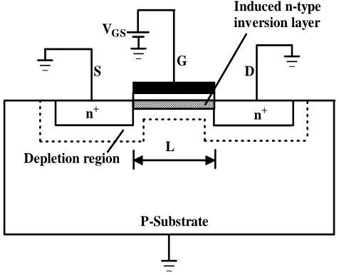
Figure 3.1 shows a cross-section of a long channel NMOS with source, drain and
bulk terminals grounded. As the gate voltage is increased from 0V, depletion region is
created below the gate. As the gate voltage is increased further, a condition of strong
inversion is reached wherein the silicon surface inverts from p-type material to n-type. This
phenomenon of strong inversion occurs at a critical value of gate-source voltage, which is
termed as the threshold voltage, VT H[Zhang05].
The threshold voltage is a function of following three voltage components:
- the difference in work function between gate and substrate (φM S)
- the fixed oxide charge present at the Si−SiO2 interface (−QOX/COX)
- the gate voltage required to bring the surface potential to the strong inversion condition
(2φF) and to offset the induced depletion region charge (−QB/COX). φF is called Fermi
potential. Typical value of φF for p-type silicon substrate is -0.3V. COX is gate oxide
capacitance per unit area.
Putting the above three components together, the threshold voltage under no body
VT H =VT HO =φM S−
QOX
COX
+ 2φF −
QB
COX
(3.1)
With no body bias (VSB = 0V), the charge stored in depletion region under the
strong inversion condition can be expressed as
QB =QBO =−
p
2qNAsi|2φF| (3.2)
where q is the electron charge, NA is doping concentration and si is the permittivity of
silicon. A body effect coefficient γ is defined as γ = √2qNAsi/COX. Thus equation 3.1
can be simplified using equation 3.2 and γ as
VT HO =φM S−
QOX
COX
+ 2φF +γ
p
2φF (3.3)
3.1.1 Body Effect
Under body biasing condition (VSB 6= 0V), the surface potential required for strong
inversion increases from|2φF|to|2φF+VSB|and the charge stored in the depletion region
is given by[Zhang05]
21
L
P-Substrate
n+ n+
D
Depletion region
Induced n-type inversion layer
S VGS
G
Figure 2.1: The cross-section of an n-MOS with positive gate voltage applied showing the depletion region and the inversion layer [1]. G is gate, D is drain and S is source.
QB=−
p
2qNAsi|2φF +VSB| (3.4)
The threshold voltage under different body biasing conditions can then be written as follows
VT H=VT HO+γ
p
|2φF +VSB| −
p
|2φF|
(3.5)
From the above equation, it is clear that for NMOS transistor, applying reverse bias voltage
(VSB >0V) to substrate-source junction of a transistor widens the source-junction depletion
region and leads to an increase in the threshold voltage. Forward body bias (VSB <0V)
reduces the depletion region and lowers the threshold voltage. This change in threshold
voltage from its nominal value VT HO due to non-zero source-substrate voltage is called as
body effect and it can be given by
∆VT H =VT H−VT HO=γ
p
|2φF +VSB| −
p
|2φF|
(3.6)
where γ = √2qNAsi/COX and COX = OX/TOX. Thus, body effect becomes less
pro-nounced for thinner oxides, higher gate dielectric constants and lightly doped substrates.
As a result, body biasing becomes less effective in every new technology generation. The
efficiency of body biasing further decreases in scaled devices due to short channel effects,
which are discussed in the following section.
3.2
Short Channel Effects
Equation (3.5) shows that the threshold voltage is a function of the manufacturing
process and the body bias voltage VSB. Threshold voltage is therefore, independent of the
channel length and the drain bias. This holds true for long-channel devices, where drain
and source depletion regions have no impact on the surface potentials or field patterns.
In short-channel devices, source and drain depletion regions penetrate more into
the channel and deplete more region under the inversion layer. These deeper depletion
the surface potential. Hence, lesser gate voltage is sufficient to cause strong inversion and
device can conduct more current than that predicted by the long-channel device equations.
This phenomenon is known as short-channel effect[Rabaey04]. As a result of short-channel
effect, the threshold voltage of a short-channel transistor depends on channel length and
drain-source voltage. Variation in the threshold voltage due to these parameters is explained
in the following subsections.
3.2.1 VT H Roll-Off
In the derivation of threshold voltage equation, it is assumed that all the depletion
region charge (QB) is induced by the applied gate voltage. This assumption is not true
in short-channel devices, in which widths of source and drain depletion regions become
comparable to the effective channel length. Fraction of the total depletion charge (∆QB)
is supplied by the drain and source depletion regions. As the channel length continues to
shrink, ∆QB increases. Therefore, a smaller gate voltage is enough to offset the remaining
depletion charge and reach strong inversion condition. As a result, threshold voltage of a
short-channel device decreases with decrease in gate length. The reduction in the threshold
voltage with decreasing device length in short-channel devices is called VT H roll-off.
3.2.2 Drain Induced Barrier Lowering (DIBL)
For a fixed source-bulk voltageVSB, raising the drain-source voltageVDS increases
the width of the depletion region around the drain-substrate junction. Hence, drain
deple-tion region contributes more depledeple-tion charge (∆QB) in short-channel devices. As a result,
smaller threshold voltage is sufficient to reach the strong inversion condition[Rabaey04].
This reduction in threshold voltage with increasing drain bias is known as drain induced
barrier lowering (DIBL) effect. DIBL effect increases the subthreshold leakage. It is a major
problem in dynamic memory circuits, where it appears as a data-dependent noise source.
From the above discussion it is clear that the short-channel effects can be
min-imized by reducing the width of source and drain depletion regions. In deep submicron
devices, this is achieved by inserting highly doped structures, called ’halo’ implants, near
3.3
Effect of Body Biasing on Leakage Components
In order to reduce leakage during standby mode using body biasing, it is important
to understand the impact of body bias on major leakage components. The primary leakage
mechanisms have been discussed in the previous chapter. In this section the variations of
these leakage components with body bias is discussed.
Taking into account the body effect and DIBL effect, SPICE BSIM4 model for the
subthreshold leakage current is as follows[Li05]
ISU B =Aexp
VGS−VT HO−γ0VSB+ηVDS
nVT
1−exp
VDS
VT
(3.7)
where A =µ0CoxLef fW VT2e1.8, VT is thermal voltage, γ0 is the linearized body effect
coeffi-cient,η is DIBL coefficient and Lef f is effective channel length.
Under reverse bias conditions (VSB >0V),γ0VSB is positive and the subthreshold
leakage decreases exponentially with increasing reverse bias. Hence, application of reverse
body biasing in standby mode can significantly reduce the subthreshold leakage. On the
other hand, forward bias (VSB < 0V) makes the γ0VSB term negative thereby increasing
the subthreshold current.
As mentioned in chapter 2, the gate leakage current density can be given by[Agarwal05]
Jgate=A·
VOX TOX 2 ·exp "
−B1−(1−VOX/φB) 3/2 VOX/TOX
#
where A = q3/16π2hφB, B = 4 √
2moxφ3B/2/3hq, φB is the tunneling barrier height in eV
and mox is effective carrier mass in oxide.
Gate leakage has an exponential dependence on the thickness of the gate oxide
(TOX) and the voltage across it (VOX). Both these parameters do not directly depend
on substrate bias. The body bias only affects the gate-to-substrate component (Igb) of
total gate leakage. However, this component is much smaller in magnitude compared to
gate-to-channel (Igc) or gate-to-source/drain overlap (Igso/Igdo) components. Hence, gate
leakage is almost insensitive to body biasing. However, gate leakage is becoming increasingly
important in nanoscale devices due to reduced oxide thickness and needs to be controlled
BTBT leakage current density is given by[Neau03]
JBT BT =A
EVRB
Eg1/2
exp −BE
3/2
g
E !
whereVRB is the reverse bias voltage applied across the junction. The electric fieldEacross
the junction is given by[Neau03]
E=
s
2qNAND(VRB+ ΨB)
si(NA+ND)
With increase in VRB (reverse bias), BTBT leakage increases since the electric field E
depends on reverse bias. BTBT leakage also depends on doping profiles. Strong halo
implants located close to to the source and drain region cause significant rise in BTBT
leakage with reverse bias.
Figure 3.2 shows the effect of body biasing on different leakage components at
room temperature for a NMOS transistor in 90-nm technology. It can be observed that
subthreshold leakage and BTBT leakage have exponential but opposite dependence on body
bias. 0.00E+00 5.00E-09 1.00E-08 1.50E-08 2.00E-08 2.50E-08 3.00E-08 3.50E-08
-0.5 -0.3 -0.1 0.1 0.3 0.5
Cu rr e n t ( A /u m )
Body Voltage (V)
Effect of Body Bias on Leakage Components
BTBT Leakage
Subthreshold Leakage
Gate Leakage
Total Leakage
3.4
Optimum Reverse Body Bias for Minimum Standby
Leak-age
Figure 3.2 shows that there exists an optimum reverse body bias voltage for which
the total standby leakage is minimized. The subthreshold leakage and BTBT leakage have
opposite dependence on body bias. Gate leakage is almost insensitive to body bias. Hence
the standby leakage is minimized at the reverse bias voltage for which the sum of BTBT
leakage and subthreshold leakage is minimum. Since both types of leakage are exponentially
dependent on body bias, the optimum reverse bias occurs when the subthreshold current
and BTBT current are approximately equal[Keshavarzi99].
In any process technology, it is difficult to correctly determine the ratio of ISU B
and IBT BT, due to process variations and complexity in calculating the electric field across
the junction. In addition, the ratio varies with each technology and doping profile[Neau03].
As a result, the location of the optimum body bias is highly dependent on technology,
doping profiles and temperature. Hence in order to find the optimum reverse body bias,
it is necessary to develop a leakage monitor circuit, which can compare the subthreshold
leakage and the BTBT leakage.
3.4.1 Previously Designed Leakage Comparator Circuits
Circuits for comparing ISU B andIBT BT have been designed in [Neau03] and
[No-mura06]. The schematic of current mirror based comparator from [Neau03] is shown in
Figure 3.3. The circuit detects body bias where the BTBT leakage is half of the total
leak-age. It mirrors half the drain current of left side NMOSN1 into the right side using PMOS
current mirror at the top. The drain current of transistor N1 mainly consists of the
sub-threshold leakage (ISU B), BTBT leakage (IBT BT) and the drain-to-gate leakage component
of gate leakage (IDG). The subthreshold leakage throughN2 is significantly lower due to the
stack effect. TheN2 leakage therefore, primarily consists ofIBT BT andIDG. Assuming the
gate leakage to be negligible and that the subthreshold leakage ofN1 andN2 are identical,
the voltage at nodes A and B, VA and VB, would depend on the BTBT currents through
transistorsN1 and N2 respectively. The two voltages would be equal when the N2 leakage
N1
N3
N2
P1 P2
VA VB
ISUB+ IBTBT+ IDG
VBN
VBN
VBN
W1 W1/2
(ISUB+ IBTBT+ IDG) /2
IBTBT+ IDG
(ISUB– IBTBT - IDG)/2
The circuit has a few problems that affect the accurate comparison of ISU B and
IBT BT. Gate leakage has been ignored in the calculation. Considering gate leakage
intro-duces error in the output current as shown in Figure 3.3. As it is clear from the discussion
of previous chapter, gate leakage is becoming increasingly important in nanometer
tech-nologies and hence should be subtracted from the current mirrored into the right side of
the circuit.
In short-channel devices, the accuracy of the current mirror depends on the
drain-to-source voltages of PMOS devices due to channel length modulation. In this circuit, there
is no provision to keep the voltages ofVA andVB constant. Any drop in the drain voltage
would result in an error in mirroring the total leakage current. To avoid this error, the drain
voltages of current mirror transistors should be held constant. Finally, the circuit does not
take into account gate-to-bulk leakage component (IGB) while calculatingIBT BT.
[Nomura06] has proposed a better leakage comparator circuit, which takes into
considerationIGB andIDG. The circuit , shown in Figure 3.4, compares the leakage current
at the source terminal of N1 with the leakage current at the drain terminal ofN4. NMOS
and PMOS current mirrors are used to mirror leakage currents. Two operational amplifiers
are used to maintain the drain voltages of current mirror transistors constant. The circuit
compares the subthreshold leakage with BTBT leakage, which includesIGB.
This leakage monitor improves accuracy by considering the gate leakage of NMOS
transistors. However, it ignores the input leakage currents of amplifiers used to keep the
drain voltages constant. Input leakage of amplifier reduces the leakage current on left side
toISU B+IDG−IGB −IIL, where IIL is the input leakage of amplifier. On right side, the
input leakage is added to the NMOS leakage (IGIDL+IDG). As a result, the comparator
output current has an error of 2IIL.
Secondly, the two components of BTBT leakage, IGIDL and IGB, are obtained
from two different NMOS transistors. The final value of IBT BT is the summation of these
two components mirrored through NMOS and PMOS current mirrors. This leads to an
erroneous value of IBT BT due to mismatches in individual transistors and the current
mir-rors. To avoid this error, it would be better if total BTBT leakage can be calculated from
3.4.2 Proposed Leakage Comparator Circuit
A new leakage comparator is proposed to improve the accuracy in estimating
the difference between the subthreshold leakage and the BTBT leakage. The schematic
of the proposed leakage comparator is shown in Figure 3.5. BTBT leakage is measured
using a single transistor on left side with drain, source and gate connected together. This
arrangement combines IGIDL and IGB to generateIBT BT. The currents in different parts
of the circuit are marked in the schematic.
As mentioned in chapter 2, BTBT leakage depends on the voltage across the
junction (VRB) and gate leakage depends on the voltage across the oxide (VOX). Hence to
find out the maximum BTBT and gate leakage, bothVRB andVOX should be maintained at
VDD, the maximum voltage difference across the junction and the oxide. This is achieved
using an amplifier, shown in Figure 3.6, with one input connected to VDD. The input
leakage of the two amplifiers cancel each other out, thus reducing the error in output current
(ISU B−IBT BT). Figure 3.7 shows the results of this comparator for increasing reverse bias
voltage. The percentage error between the simulated and the calculated leakage currents
N3
P1 P2
IBTBT(= IGIDL+ IGB) – ISUB + 2IIL
VBN
VBN
IGIDL+ IDG + IIL
N2
VBN
N1
VBN
IGB
ISUB+ IDG
-IGB
VDDM VDDM
VDDH
VDD VDD
+
_ IIL
ISUB+ IDG– IGB -IIL
IGIDL+ IDG
IIL
_
+
N4
N3
P3 P4
VBN
VBN
ISUB- IBTBT
N1
VBN
VDDH
VDD
+ _
IIL
_
+ P1 P2
VDDH
N2
IBTBT + IIL
IIL
IGB
IGIDL IDG IDG
ISUB
IIL+ ISUB+IDG
ISUB+ IDG
– IBTBT
VDD
Vin+
Vbias
Vin-Vout VDD
P1
P2
N1 N2
N3
is always below±5% for the range−1V to 0V of VBS. The results indicate that the point
of minimum leakage (ISU B = IBT BT) occurs at VBS = −0.88V. Table 3.1 compares the
performance of the designed leakage monitor with the previously discussed leakage monitor
circuits. -5 0 5 10 15 20 25 30 35 40
-1 -0.8 -0.6 -0.4 -0.2 0
C u rr e n t (p A )
VBS(V) Error -5 -4 -3 -2 -1 0 1 2 3 4 5
-1 -0.8 -0.6 -0.4 -0.2 0
P e rcen ta g e ( % )
VBS(V)
Percentage Error
Figure 3.7: Leakage Monitor Results
3.5
Standby Leakage Reduction using Reverse Body Bias
90-nm process technology provides devices with nominal threshold
Table 3.1: Performance of the leakage monitor circuits
Parameters [Neau03] [Nomura06] This work
Range of VBS −0.2V to 0.2V −1.5V to 0V −1V to 0V
Percentage Error 35% <20% <±5%
Supply Voltage Range 0.6V to 0.8V 0.4V to 1V 1V to 1.2V Device Technology Used 50-nm, 70-nm 90-nm 90-nm
Gate Leakage ignored considered considered
BTBT Leakage Measured only IGIDL bothIGIDL andIGB both IGIDL and IGB
Amplifier Input Leakage - ignored considered
Table 3.2: Devices Used for Body Biasing
Parameters Reg-VT H Low-VT H
Gate Length 80nm 80nm
Oxide Thickness 2.2nm 2.2nm
VT H (NMOS/PMOS) (370mV/315mV) (250mV/190mV)
Body Effect Coefficient (NMOS/PMOS)) (114mV/100mV) (90mV/50mV)
Nominal Supply Voltage 1V 1V
for low power, high speed applications. Table 3.2 lists the important device parameters for
both types of devices.
For a single NMOS or PMOS transistor, the off-state leakage is primarily governed
by the subthreshold leakage. The low-VT H devices exhibit considerably higher subthreshold
leakage than the reg-VT Hdevices. Due to its exponential dependence on reverse bias voltage,
the off-state leakage decreases rapidly with increasing reverse bias voltage as shown in Figure
3.8 and 3.9.
In static CMOS circuits, on-state gate leakage is comparable to the total off-state
leakage [Arnim05]. Hence, both on and off states of the circuit should be considered while
calculating the total leakage of a CMOS circuit. Figure 3.10 shows the effect of reverse
body bias on the total leakage of an inverter pair. Although, reverse body bias significantly
reduces the total leakage of low-VT H inverter pair, it is always higher than the reg-VT H
counterpart. The leakage of low-VT H inverter pair is twice as much that of reg-VT H even
at the most negative body bias.
To check the efficiency of reverse body bias in leakage reduction, an optimum
reverse body bias voltage, detected using the leakage monitor, is applied to several static
Off State Leakage of NMOS Device 0.00 0.50 1.00 1.50 2.00 2.50 3.00 3.50 4.00
-1.00 -0.80 -0.60 -0.40 -0.20 0.00
VBS (V)
Cu rr e n t (n A /u m ) Reg-Vt Low-Vt
Figure 3.8: NMOS Off State Leakage Current
Off State Leakage of PMOS Device
0.00 2.00 4.00 6.00 8.00 10.00 12.00 14.00
-1 -0.8 -0.6 -0.4 -0.2 0
VSB (V)
C u rr e n t (n A/ u m ) Reg-Vt Low-Vt
Figure 3.9: PMOS Off State Leakage Current
Inverter Leakage 20.00 70.00 120.00 170.00 220.00 270.00
-1.00 -0.80 -0.60 -0.40 -0.20 0.00
NMOS Body Bias (V)
Cu rr e n t ( n A) Reg-Vt Low-Vt
Table 3.3: Leakage Reduction Using Reverse Body Bias for Reg-Vt Devices
Circuit VBS = 0V VBS = -0.88V Percentage Reduction
NMOS 1.13nA 46.67pA 95.87%
PMOS 5.482nA 460pA 91.6%
Inverter Pair 8.27nA 614.8pA 92.56%
2-input NAND 27.26nA 25.42nA 6.75%
2-input NOR 26.84nA 20.56nA 30.54%
Table 3.4: Leakage Reduction Using Reverse Body Bias for Low-Vt Devices
Circuit VBS = 0V VBS = -0.88V Percentage Reduction
NMOS 13.16nA 1nA 92.4%
PMOS 190.9nA 57.88nA 69.68%
Inverter Pair 205.8nA 55.64nA 72.96%
2-input NAND 45nA 25.51nA 43.31%
2-input NOR 208.1nA 78.4nA 62.32%
reduction. Tables 3.3 and 3.4 list the reduction in leakage current due to applied optimum
reverse bias. For NAND and NOR gates, the worst case standby leakage is considered
depending on the input sequences.
The results indicate that the reverse body bias is less effective for the low-VT H
devices than the reg-VT H devices, mainly due to the lower body effect coefficient. In case
of PMOS transistors, the body effect parameter for low-VT H device is 44.44% lower than
the reg-VT H counterpart (See Table 3.2). As a result, the leakage reduction achieved using
reverse bias is considerably lower for low-VT H transistor. To maintain the efficiency of body
biasing, higher reverse bias voltage would be required for low-VT H devices. However, at
higher reverse bias voltages, the effectiveness of this technique decreases due to square root
dependence of threshold voltage on body bias[Arnim05].
3.5.1 Leakage Reduction in Stacked Transistors Configurations
Table 3.3 and 3.4 show that the efficiency of reverse body bias decreases with
transistor stacking. For NAND and NOR gates the worst case standby leakage occurs when
all the transistors in the stack are conducting except the topmost transistor (See Table
2.1 for the standby leakage in a 2-input NAND gate). As discussed in chapter 2 (section
internal node voltages are close to ground potential. The total standby leakage is given by
the sum of the dominant gate leakage and the subthreshold leakage of the nonconducting
topmost transistor. Since gate leakage is independent of the reverse bias, the reduction
in standby leakage is much less in the stacked transistors configuration. As mentioned in
chapter 2, gate leakage of PMOS device is an order of magnitude lesser than that of NMOS
device. As a result, percentage reduction in leakage is higher in a NOR gate than a NAND
gate.
In case of low-VT H circuits, the total leakage is dominated by the subthreshold
leakage of the topmost transistor. Therefore, the percentage reduction in total leakage
using reverse biasing is higher in low-VT H NAND and NOR gates. From the results of Table
3.3 and 3.4, reverse biasing looks more effective in high speed circuits using smaller VT H
transistors[Arnim05]. In such circuits, reverse biasing reduces the dominant subthreshold
leakage thereby decreasing the total standby leakage.
3.6
Dynamic Performance Improvement Using Forward Body
Bias
Forward body bias in active mode increases the on-state current by reducing the
threshold voltage. This results in higher speed and better dynamic performance. Figure
3.11 and 3.12 show the effect of body bias on the on-state current of NMOS and PMOS
devices respectively.
5-stage ring oscillator and 16-bit ripple carry adder have been used as test
struc-tures to study the effect of forward body bias on speed. Table 3.5 and 3.6 show the speed
improvement for a 5 stage ring oscillator and 16-bit ripple carry adder under 0.3V of forward
body bias.
The results indicate that only slight performance improvement can be achieved
using forward body bias. Therefore, body biasing is less effective in improving speed of the
circuit in active mode. There are additional difficulties in implementing forward body bias.
Latch-up has to be avoided over operating temperature and process variations. Leakage
currents, especially the subthreshold leakage grows exponentially with the forward bias.
2.00 2.20 2.40 2.60 2.80 3.00 3.20 3.40 3.60 3.80
0.00 0.10 0.20 0.30 0.40 0.50
Cu rr e n t ( m A )
VBS(V)
NMOS On state current vs body bias
Reg-Vt
Low-Vt
Figure 3.11: Increase in on-state current of NMOS device with forward body bias
8.00E-04 9.00E-04 1.00E-03 1.10E-03 1.20E-03 1.30E-03 1.40E-03 1.50E-03
0.00 0.10 0.20 0.30 0.40 0.50
C u rre n t ( A )
VSB (V)
PMOS ON state current vs body bias
Reg-Vt Low-Vt
Table 3.5: Performance Improvement using Forward Body Bias for Reg-Vt Devices
Circuit VBS = 0V VBS = 0.3V Percentage Improvement
NMOS 2.213mA 2.479mA 12.01%
PMOS 3mA 3.287mA 9.56%
Ripple Cary Adder 50ps 45.53ps 8.94%
Ring Oscillator 15.19MHz 16.59MHz 9.2%
16-bit Adder 1.428ns 1.316ns 7.84%
Table 3.6: Performance Improvement using Forward Body Bias for Low-Vt Devices
Circuit VBS = 0V VBS = 0.3V Percentage Improvement
NMOS 3.128mA 3.358mA 7.35%
PMOS 4.372mA 4.56mA 4.3%
Ripple Cary Adder 34.5ps 32.9ps 4.63%
Ring Oscillator 33.39MHz 34.87MHz 4.43%
16-bit Adder 983.5ps 960.4ps 2.34%
body biasing techniques is less practical in large integrated circuits implemented in nanoscale
devices. As a result, other circuit techniques should be used for improving the dynamic
performance of the circuit. Supply voltage scaling, which can reduce the dynamic power