ABSTRACT
NACKASHI, DAVID PETER. Circuit and Integration Technologies for Molecular Electronics. (Under the direction of Paul D. Franzon.)
Methods for fabricating a 2D array of gold nanoparticles were investigated for the
purpose of creating a cross-linked molecular network. A controllable process for quickly and
easily depositing and patterning regions of gold nanoparticles was developed. This process
involves first patterning gold electrodes used for electrical measurement on the wafers.
Regions are then defined in photoresist where the dense gold nanoparticles are desired.
Finally, the nanoparticles are deposited using a short evaporation, resulting in island
formation through the Volmer-Weber growth mechanism. The resist is then stripped in a
process known as liftoff, and the result is a wafer-scale substrate with well-defined regions
for molecular interconnect. Before assembly, these structures conduct less than 110pA of
current at submicron electrode gap distances, and often less than 20pA.
As determined from SEM image analysis, it is possible to quickly and easily deposit
and pattern regions on silicon dioxide containing over 4,100 per µm2, each with an average
area of approximately 80nm2. The number of particles, average area and fill density can be
controlled to allow for a number of applications and at a variety of scales. The smaller, more
numerous particles integrate into sub-500nm gaps, and the larger, meandering lines integrate
CIRCUIT AND INTEGRATION TECHNOLOGIES FOR
MOLECULAR ELECTRONICS
by
DAVID PETER NACKASHI
A dissertation submitted to the Graduate Faculty of North Carolina State University
in partial fulfillment of the requirements for the Degree of Doctor of Philosophy
ELECTRICAL ENGINEERING
Raleigh, NC
2004
Copyright © 2004 David Peter Nackashi
All Rights Reserved
Figures 11,14,15,21 and 30 reprinted with permission. Copyright © 1998, 2001, 2002, 2003 American Chemical Society.
Figures 3, 4, 5, 12 and 13 reprinted with permission. Copyright © 1996, 2002 American Physical Society. Figures 17 and 18 reprinted with permission. Copyright © 1995 Elsevier.
Figures 16 and 24 reprinted with permission. Copyright © 2003 IOP Publishing Ltd. Figures 1, 29 and 42 reprinted with permission. Copyright © 2001, 2002, 2003 IEEE Figure 6 reprinted by permission from Nature. Copyright © 2000, Macmillan Publishers Ltd.
Figures 9, 10, 22, 23, 25, 26, 27 and 28 reprinted with permission. Copyright © 1997, 2001, 2003 The American Association for the Advancement of Science.
Figures 7 and 8 reprinted with permission. Copyright © 1998, The Annals of the New York Academy of Sciences.
DEDICATION
I would like to dedicate this work to my wife, Beth, whose never-ending patience continues to amaze me. Her ability to listen to me talk nightly over dinner about topics that bore most everyone to tears is one I greatly appreciate and can only admire. Her constant source of encouragement and patience as the years rolled by inspired me to stay driven and keep focused (at least most of the time.)
BIOGRAPHY
David Peter Nackashi, son of David and Cindy Nackashi, was born in Tampa, FL, June 18th, 1971. He was raised in Macon, GA and graduated high school from Mount de Sales Academy in 1989. David attended college at the Georgia Institute of Technology, where he graduated with a Bachelor of Electrical Engineering in 1993.
After graduation, David worked for Alcatel Telecom in Raleigh, NC for almost six years. While at Alcatel, he worked in several different departments including System Integration and Verification where he served as Team Leader during development of the 1603/12/48 SMX Release A.A, an OC-48 SONET Multiplexer. Working at Alcatel, David attended North Carolina State University and received his Master of Science in Computer Engineering in 1999. He then left Alcatel to study full-time for his Ph.D.
ACKNOWLEDGEMENTS
The completion of this research was in large part due to the support of many, many people at N.C. State. I would like to acknowledge the follow individuals for both their patience and support.
Dr. Paul Franzon. Paul is the first professor I met at N.C. State, and taught the first class I took here: Digital ASIC Design. His enthusiasm in the classroom drew me to his research group, where I studied under him for my Ph.D. Having worked in industry for a number of years prior to becoming a full-time student (for the second time in my life), I was instantly drawn to the level of confidence and professionalism he consistently shows towards his students. Paul, without exception, encouraged me to explore less conventional paths in electrical engineering, and supported my work providing valuable direction along the way. I owe the richness of my graduate experience to Paul, and will be forever thankful that he made a place for me in his group.
My committee members, including Dr. Greg Parsons of the Department of Chemical Engineering, Dr. John Muth and Dr. Veena Misra of the Department of Electrical and Computer Engineering. Dr. Parsons and Dr. Misra were always available for discussions, and together taught a class on Nanotechnology which I thoroughly enjoyed. I am especially appreciative of Dr. Muth and the many conversations over lunch. We always began with the intent to discuss one topic and usually ended up in an entirely different area, but I always left with a better understanding of some interesting aspect of physics.
addition, Neil Di Spigna and Chris Amsinck, students in our molecular electronics group who I appreciate discussing my research with. I’ve enjoyed watching you learn and will enjoy even more watching you graduate. Also, I would like to thank John Wilson, Steve Lipa and David Winick, whose technical knowledge in device characterization and analysis spanning RF to optical made gathering data a much less difficult task than it could have been. Many thanks to past students Toby Schaffer and Alan Glauser whose work in developing an incredible Cadence Design Kit helped layout and simulation go smoothly. Finally, a special thanks to Michele Joyner who makes everything happen up here on the fourth floor.
I would also like to thank the staff of the NCSU Nanofabrication Facility, especially Joan O’Sullivan, Ginger Yu, Harold Morton and Henry Taylor. I appreciate your patience while I learned new skills, and would certainly have never been able build such a large variety of devices without your help and support. I would like to thank Dale Bachelor and Roberto Garcia of the Analytical Instrumentation Facility, who provided me with a great deal of support while learning how to prepare and image my samples.
TABLE OF CONTENTS
LIST OF TABLES... x
LIST OF FIGURES ... xi
LIST OF SYMBOLS OR ABBREVIATIONS ... xviii
1 INTRODUCTION ... 1
1.1 Motivation for Molecular Electronics... 1
1.1.1 Thermodynamics... 1
1.1.2 Impending Issues Confronting Current CMOS Devices ... 3
1.2 Brief Overview of Research and Novel Claims... 5
1.3 Dissertation Outline ... 6
1.4 Relevant Publications and Patents ... 7
2 LITERATURE REVIEW ... 9
2.1 Motivation and Issues in Molecular Electronic Technologies... 9
2.2 Transport and Modeling of Devices ... 12
2.3 Device Characterization, Nanostructures and Test Beds... 17
2.3.1 Simple Molecular Self-Assembly ... 19
2.3.2 Object and Molecular Assembly... 29
2.3.3 Physical Vapor Deposited Top Contact... 34
2.3.4 STM Analysis ... 37
2.4 Architectures: Computation and Memory ... 42
2.5 Conclusion ... 50
3 CIRCUITS AND SCALABILITY ... 51
3.1 Bistability and Negative Differential Resistance... 51
3.1.1 The Goto Pair... 52
3.3 Isolation... 62
3.4 Conclusion ... 64
4 DESIGN AND FABRICATION OF MOLECULAR CROSS-LINKED NETWORKS 66 4.1 The Nanocell as a Cross-Linked Network ... 66
4.2 Challenges and Assumptions in Modeling the Nanocell ... 69
4.3 Implementation Goals... 71
4.4 Colloid-Based Molecular Networks ... 73
4.4.1 Design and Fabrication ... 74
4.4.2 Experimental Results ... 79
4.4.3 Experimental Conclusions ... 83
4.5 Discontinous Gold Film Molecular Networks... 84
4.5.1 Design and Fabrication ... 85
4.5.2 Experimental Results ... 90
4.5.3 Experimental Conclusions ... 95
4.6 Scaling of Discontinuous Gold Film Molecular Networks and other Metal Systems 95 4.6.1 Design and Fabrication ... 96
4.6.2 Experimental Results ... 104
4.6.3 Experimental Conclusions ... 108
5 DISCONTINUOUS GOLD FILM MEASUREMENT AND ANALYSIS... 110
5.1 Fabrication of Samples to Investigate Gold Island Morphology... 110
5.2 Morphology of Island Formation using Scanning Electron Microscopy... 113
5.2.1 Scanning Electron Microcopy Imaging ... 113
5.2.2 Image Manipulation... 117
5.2.3 Statistical Results... 122
5.3 Morphology of Island Formation using Atomic Force Microscopy... 134
5.4 Statistical Conclusions... 137
6 CONCLUSIONS AND FUTURE WORK ... 139
6.1 Conclusions and Novel Claims... 139
6.2 Future Work and Applications... 140
REFERENCES ... 144
APPENDICIES... 157
A ELECTRON BEAM INTERACTIONS FOR DISCONTINUOUS GOLD FILMS.... 158
A.1 Introduction... 158
A.2 Materials and Assumptions... 159
A.2.1 Description of Sample... 159
A.2.2 Simulator Choices... 160
A.2.3 Simulator Parameters and Assumptions ... 160
A.3 Simulation Results ... 161
LIST OF TABLES
Table 1: NCSU Test Chip Revision 1 Process Flow for Polyimide (left) and SOG(right)
devices... 76
Table 2: Experimental conditions for leakage current measurements ... 80
Table 3: Nanocell Test Chip Revision 2 Process Flow - Contact Lithography ... 86
Table 4: Nanocell Test Chip Revision 3 Process Flow - Projection Lithography ... 97
Table 5: Number of Particles and Error Calculations (threshold bias)... 125
Table 6: Island Area Statistics (Wet Oxide) ... 131
Table 7: Island Area Statistics (Dry Oxide)... 131
Table 8: Island Perimeter Statistics (Wet Oxide) ... 131
Table 9: Island Perimeter Statistics (Dry Oxide)... 131
Table 10: Number of Islands (Wet Oxide) ... 132
Table 11: Number of Islands (Dry Oxide)... 132
Table 12: Ra for DGF on Wet Oxide ... 136
LIST OF FIGURES
Figure 1: Energy required to perform a logic operation. ... 3
Figure 2: Self-assembly required for various architectures ... 11
Figure 3: Metal-Molecule-Metal junction. From Samanta et al.34, "Electronic conduction through organic molecules." ... 13
Figure 4: Green-function analysis of electronic transmission through different molecules. From Samanta, et al.34, "Electronic conduction through organic molecules."... 15
Figure 5: Ring orientation effects on the tranmission property. From Samanta, et al.34,
"Electronic conduction through organic molecules." ... 16
Figure 6: Suggested molecular electronic devices. From Joachim et al.26, "Electronics using hybrid-molecular and mono-molecular devices."... 17
Figure 7: Catagories of Molecular Test Structures. From Allera et al.16, “Evolution and Strategies for Self-Assembly and Hookup of Molecular-Based Devices.” ... 19
Figure 8: Orientation of molecules between two probes. From Allera et al.16, “Evolution and Strategies for Self-Assembly and Hookup of Molecular-Based Devices.” ... 20
Figure 9: Mechanically-controlled break junction (MCB). From Reed et al.46, “Conductance of a Molecular Junction.”... 21
Figure 10: Assembly and electrical data from the MCB. From Reed et al.46 "Conductance of a Molecular Junction." ... 22
Figure 11: Crossed wire tunnel junction. From Kushmerick et al.49, "Effect of Bond Length Alternation in Molecular Wires"... 23
Figure 12: OPEs investigated. From Kushmerick et al.48, "Metal-Molecule Contacts and Charge Transport across Monomolecular Layers: Measurement and Theory" ... 24
compound 1, and (b) is compound 2. From Kushmerick et al.48, "Metal-Molecule Contacts and Charge Transport across Monomolecular Layers: Measurement and
Theory" ... 24
Figure 14: I-V plotted as function of deflection current. From Kushmerick et al.50,
"Conductance Scaling of Molecular Wires in Parallel"... 25
Figure 15: Au-C16//C16-Hg junction. From Holmlin, et. al.56, "Electron Transport through
Thin Organic Films in Metal-Insulator-Metal Junctions Based on Self-Assembled
Monolayers."... 27
Figure 16: Trapped colloids using dielectrophoresis. From Rawlett et al.60, "A molecular electronic toolbox."... 29
Figure 17: 2D matrix of 4nm gold particles. From Janes et al.63, "Electronic conduction through 2D arrays of nanometer diameter metal clusters.” ... 30
Figure 18: Crosslinked 2D cluster electrical response. From Janes et al.63, "Electronic
conduction through 2D arrays of nanometer diameter metal clusters.”... 31
Figure 19: Gold clusters deposited at (a) 25oC, 3s (b) 160oC, 8s (c) 200oC, 8s (d) 250oC, 8s. From Parmigiani et al.72, "Optical properties of sputtered gold clusters." ... 33
Figure 20: Nanopore. From Zhou et al.51, "Nanoscale metal/self-assembled monolayer/metal heterostructures." ... 35
Figure 21: Inserted molecular wire into an alkanethiol matrix. From Cygan et al.45, "Insertion, Conductivity and Structures of Conjugated Organic Oligomers in Self-Assembled Alkanethiol Monolayers on Au{111}." ... 38
Figure 22: STM contacts to groupings of molecules. From Cui et al.35, "Reproducible
Measurement of Single-Molecule Conductivity." ... 39
Figure 23: Switching in OPEs. From Donhauser et al.95, "Conductance Switching in Single Molecules Through Confirmational Changes." ... 41
Figure 24: 8x8 memory array. From Chen and Williams et al.23, "Nanoscale molecular-switch crossbar circuits." ... 43
Figure 25: SNAP process. From Melosh, Heath et al.104, "Ultrahigh-Density Nanowire Lattices and Circuits."... 44
Figure 26: Patterning of Pt nanowires using SNAP. From Melosh, Heath et al.104,
Figure 27: Directed nanowire assembly. From Huang, Lieber et al.98, "Directed Assembly of
One-Dimensional Nanostructures into Functional Networks." ... 46
Figure 28: Nanowire logic gates. From Huang, Lieber et al.106, "Logic Gates and Computation from Assembled Nanowire Building Blocks."... 47
Figure 29: Nanocell schematic. From Tour et al.17, "Nanocell Logic Gates for Molecular Computing."... 48
Figure 30: Nanocell device after assembly. From Tour et al.77, "Nanocell Electronic Memories."... 49
Figure 31: Typical IV response of an RTD. ... 51
Figure 32: The Goto pair. Three regions in a correctly biased latch. (I) positive resistance; (II) NDR; (III) positive resistance (“rising tail”). ... 53
Figure 33: Schematic of Goto pair circuit... 54
Figure 34: Biasing of a Goto pair. ... 54
Figure 35: Biasing of the Reed NDR... 55
Figure 36: Biasing of the Reed32 data using several resistive values as loading elements... 56
Figure 37: Bistable latch simulated from Reed32 data and loaded with a 373MΩ resistor. ... 58
Figure 38: NAND (left) and NOR (right) gates; schematics at top and waveforms below.... 60
Figure 39: 2x2 memory array schematic (left) and waveforms (right)... 61
Figure 40: Effects of loading networks on Goto pairs... 63
Figure 41: Schematic of a Nanocell... 67
Figure 42: Assembly of Nanocell blocks into a four-bit adder. From Husband et al.64, "Logic and Memory with Nanocell Circuits" ... 68
Figure 43: Need for integration technologies ... 72
Figure 45: Nanocell Test Chip Revision 1 cross sections for the “Polyimide Chip” (top) and
“SOG Chip” (bottom.) ... 75
Figure 46: Nanocell Test Chip Revision 1, Top view ... 77
Figure 47: 2-sided 2-lead device (left); 2-sided 10-lead device (right). Left images are layout and right images are devices fabricated in the polyimide process... 77
Figure 48: 4-sided 20-lead device. Left image is layout and right image is device fabricated in the polyimide process ... 78
Figure 49: Colloid Deposition Experimental Summary ... 81
Figure 50: Colloid deposition (aminosilane pH7, 60nm) ... 81
Figure 51: Leakage current measurements for NCSU Test Chip Revision 1 ... 82
Figure 52: Nanocell Test Chip Revision 2 cross-section... 85
Figure 53: Edge effects from DGF liftoff patterning with a single resist stack... 87
Figure 54: Edge effects for single (left) verses double (right) photoresist stacks. ... 88
Figure 55: Nanocell Test Chip Revision 2, Top view ... 89
Figure 56: 2-sided 2-lead device (left); 4-sided 20-lead device (middle); fabricated 4-sided 20-lead device (right). The discontinuous gold film is the blue region at the center of the image... 90
Figure 57: DGF imaged at x200k. This film was deposited at an average thickness of 50Å on a 1000Å thick silicon dioxide. ... 90
Figure 58: Compound mononitro oligo(phenylene ethynylene)... 91
Figure 59: Switching behavior in DGF NanoCell. On-Off ratio for device C4, center pins, 4µm gap between electrodes. The left plot is the first sweep indicating a switching behavior, and the right plot illustrates a linear response after subsequent sweeps. ... 93
Figure 60: On-Off ratio for device C4, center pins, 4µm gap between electrodes... 93
Figure 61: Nanocell Revision 3 cross-section ... 97
Figure 63: Nanocell Test Chip Revision 3 Top View... 100
Figure 64: 2-sided 2-lead device set (left); 2-sided 2-lead 600nm device close-up (right). The red region in the center is the patterned DGF. ... 101
Figure 65: 4-sided 8-lead device; layout (left) and optical image (right). The red region in the center is the patterned DGF. ... 102
Figure 66: Multi-lead 2-sided NanoCell with dummy lines sacrificed (left). Higher
magnification of the line array (right)... 103
Figure 67: Density effects in recessed and protruding 600nm lines within an array... 103
Figure 68: SEM image of the DGF region between two electrodes (left), and the probing of this device (right). ... 104
Figure 69: IV Sweeps for 20Å verses 30Å thick DGFs as measured across varying gaps. . 105
Figure 70: Direct tunneling expression of electroncs through metallic island complexes. From Celasco125 et al. ... 106
Figure 71: 300-350Å gap between two adjacent gold electrodes (left). Red box indicates area magnified (right). The DGF was grown to an average thickness of 30Å. ... 107
Figure 72: Contact regions from thin Metal 1 to thick Metal 2... 107
Figure 73: Samples evaporated with varying amounts of thin gold on silicon dioxide. The amount of gold shown is 20Å, 30Å, 40Å, 50Å and 60Å from left to right. The
substrates (1000Å thermally grown silicon dioxide on silicon) are shown in the above row with gold regions magnified in the bottom row... 112
Figure 74: DGFs deposited at the indicated average thicknesses. The substrate is 1000Å of thermally grown (steam process) silicon dioxide on a p-type (100) 1-10 Ω-cm wafer.115
Figure 75: DGFs deposited at the indicated average thicknesses. The substrate is 37Å of thermally grown (dry process) silicon dioxide on a p-type (100) 0.01 Ω-cm wafer with a backside aluminum contact... 116
Figure 76: Original image (left) and corresponding histogram (right). ... 118
Figure 78: Pixel intensity stretched across allowable range (left) and resulting histogram (right). ... 120
Figure 79: Threshold set to 0.38 (left) and pre-threshold image overlayed with edge pixels plot (right). ... 122
Figure 80: Fill factor verses average deposition thickness (Å). Blue line indicates wet oxide sample and the gray line indicates dry oxide sample... 123
Figure 81: Number of islands verses average deposition thickness (Å). Blue line indicates wet oxide sample and the gray line indicates dry oxide sample. Total frame area is 0.389µm2... 126
Figure 82: Perimeter to Area ratio normalized to a rectangle of the same field size
(0.389µm2.) ... 127
Figure 83: 40Å average thickness on wet thermal oxide, threshold 0.38 (left) and edge
particles removed (right)... 128
Figure 84: Histograms for number of particles per area (pixels). Deposition conditions and substrate indicated in plot, with singularity identified... 129
Figure 85: Average island area with edges and singularities removed. The blue lines represent the wet oxide conditions and the grey lines the dry oxide conditions. Fewer than 77 islands exist for the 50Å and 60Å wet oxide, and once the edge and singularities are removed, as few as 5. This is not considered to be statistically enough samples for the average area calculations. ... 133
Figure 86: Average island perimeter with edges and singularities removed. The blue lines represent the wet oxide conditions and the grey lines the dry oxide conditions. Fewer than 77 islands exist for the 50Å and 60Å wet oxide, and once the edge and singularities are removed, as few as 5. This is not considered to be statistically enough samples for the average perimeter calculations... 133
Figure 87: Number of islands calculated with edges and singularities removed. The blue lines represent the wet oxide conditions and the grey lines the dry oxide conditions.. 134
Figure 88: Digital Instruments Dimension 3000 AFM height (left) and phase (right) images for 20Å DGF on wet oxide. ... 135
Figure 89: Digital Instruments Dimension 3000 AFM height (left) and phase (right) images for 60Å DGF on wet oxide. ... 135
Figure 91: Materials Stackup... 160
Figure 92: ηAu/η for Beam Energies of 0.2-1 keV ... 162
Figure 93: ηAu/η for Beam Energies of 5-20 keV ... 162
Figure 94: ηAu/η for Beam Energies of 1-5 keV ... 163
Figure 95: Monte Carlo for Beam Energy of 1.8 keV ... 164
Figure 96: Monte Carlo for Beam Energy of 4.6 keV ... 165
LIST OF SYMBOLS OR ABBREVIATIONS
AFM Atomic Force Microscopy
CCC Custom Configurable Computers
CMOS Complementary Metal Oxide Semiconductor
CNT Carbon Nanotube
DCM dichloromethane
DFT Density Functional Theory ESL Etch Stop Layer
FPGA Field Programmable Gate Array HOMO Highest Occupied Molecular Orbital
IC Integrated Circuit
ITRS International Technology Roadmap for Semiconductors LPCVD Low Pressure Chemical Vapor Deposition
LUMO Lowest Unoccupied Molecular Orbital
MOSFET Metal Oxide Semiconductor Field Effect Transistor (also abbv. FET) OPE oligo (phenylene ethnylene)
OPV oligo (phenylene vinylene) PDMS polydimethylsiloxane
RAIR reflection-absorption infrared spectroscopy RTD resonant tunneling diode
SAM Self-assembled monolayer SEM Scanning Electron Microscopy SER Soft Error Rate
SOG Spin-on Glass
STM Scanning Tunneling Microscopy
1 INTRODUCTION
1.1 Motivation for Molecular Electronics
The motivation for research exploring alternate methods for computation is most often explained as a necessity in preparing for the day when Complementary Metal Oxide Semiconductor (CMOS) technology can no longer be made more efficient6. Although this is a compelling argument, perhaps the most convincing case can be made by simply suggesting how much more room for improvement to computation efficiency is available, regardless of what that technology might be.
1.1.1 Thermodynamics
Although the exact path CMOS development will take over the next decade remains unclear, one point is certain: the theoretical physical limit to computation would not be reached even if Moore’s law were to hold true for many more decades1,2. Since Moore’s law is not a law of science, rather, a law of human ingenuity2, it is reasonable to speculate that other technologies might be developed that could result in the same computational advances that have occurred during that past fifty years. What exactly those technologies are remains to be seen.
In the mid 1950’s, von Neumann’s research3 on the role of thermodynamics in computation lead him to suggest that a logical operation performed by a computer would result in an energy dissipation of kBT*ln(2). Following von Neumann, Landauer4 later
between reversible and irreversible operations. A reversible operation is one where the initial state can be derived from the final state, providing a method for returning, or reversing, the operation itself. One example of a reversible operation is a NOT, commonly known as an inverter. An irreversible operation is one where the initial state cannot be determined by the final, therefore, no method for reversing the operation exists. Examples of irreversible operations are AND, OR, ERASE and NAND. Since it is impossible to determine the exact inputs simply by observing the output of any of these gates, information is therefore lost during the operation process. Landauer4 showed that irreversible operations must dissipate an amount of energy kT*ln(2) for each bit of information lost. From this derivation, he also proposed that a computational system created entirely of reversible elements would, in theory, dissipate no energy. Charles Bennett proved this point in 1973 by showing that a computer, built solely from reversible operations5, dissipates little to no energy. Practical limitations, however, have prevented this type of architecture from making its way into commercial products6.
Figure 1: Energy required to perform a logic operation. From Keyes6, "Fundamental Limits of Silicon Technology"
Two to three orders of magnitude improvement in computational efficiency are seen every fifteen years, so by the year 2012, computers are expected to execute 109 additions per Joule of energy7. Although unprecedented, this efficiency is nowhere near the fundamental theoretical limit. Assuming only nonreversible logical operations, approximately 100*kT*ln2 of energy is required to add two 10 digit decimal numbers, which otherwise stated is approximately 3*1018 additions per Joule at room temperature1,4,7. This implies there are nine orders of magnitude available for improvement in computational efficiency after what CMOS is expected to deliver in the year 2012.
1.1.2 Impending Issues Confronting Current CMOS Devices
more complex logical operations can be performed resulting in greater area efficiency. Second, smaller devices use fewer electrons resulting in greater power efficiency. Finally, smaller wires have lower capacitances which translate directly to higher speeds of operation. Combining these three advantages results in a continuing trend of denser, faster more power efficient computation.
Many issues face scientists and engineers if CMOS is to continue the same miniaturization trend that it has followed for the past forty years. Some of the primary challenges in scaling CMOS below 100nm will be found in lithography, power supply and threshold voltages, short-channel effects, gate oxide, high field effects, random dopant distribution and interconnect delays9.
These areas will force devices to be modeled not with scaled-down “bulk” properties, but perhaps as individual molecular elements or structures. One example occurs in dopant distribution. As devices get smaller, bulk properties no longer hold true and scattering events occur less frequently. This is because the channel width is approaching the mean free path of an electron traveling through doped silicon6, resulting in ballistic transport anomalies which make device properties difficult to predict.
Solutions for many of these problems are well underway, and as a result, many new novel semiconductor devices and technologies have surfaced such as SOI CMOS, the SiGe, Low-Temperature CMOS, and double-gate MOSFETs9. Just as these new technologies have grown from advances in many of the challenging areas listed above, it is expected that these same advances will help assist research in molecular electronics and vice versa.
As advances in CMOS continue and as new technologies for computation are researched and developed, advances in architecture will accompany them. Perhaps one of the most glaring issues confronted, as devices continue to shrink, is their susceptibility to errors and defects. This issue has been recognized by research groups in both silicon and alternative technologies, and a variety of new architectures10,11 have surfaced which promise to address the problem.
cosmic rays12. If a large enough number of erroneous hole-pairs are generated, charges in wires and memories can be altered yielding false readings10. As capacitances and supply voltages continue to shrink, the amount of charge that is both needed and used to store data shrinks as well. This makes each subsequent technology generation more susceptible to soft errors, resulting in a doubling of the soft error rate (SER) every 18 to 24 months10. In contrast, hard errors are induced by physical mistakes in the fabrication process, stemming from photolithography, etching, metallization, etc. Defects of this type directly affects production yield, therefore manufacturing cost per die. Almost regardless of the next generation technology, defect tolerance is expected to play a critical role in memory and microprocessor architecture7,10. For this reason, much of the research into molecular electronics feasibility addresses both architecture and devices. In fact, there is as much variation in the design of molecular electronic architectures as there are devices themselves.
1.2 Brief Overview of Research and Novel Claims
This research is focused on understanding and improving upon circuit and integration strategies in molecular electronics applications. One of the first published papers suggesting a molecular electronic property other than rectification was by Reed in 1999. In this work, Reed suggested that a measured current-voltage characteristic known as negative differential resistance (NDR) was the result of the 2’-amino-4-ethynylphenyl-4’ethynylphenyl- 5’nitro-1-bensenethiolate molecule, synthesized by Tour and sandwiched between two gold leads. Today, a large number of architectures are based upon using NDR to create logic gates, memories and switches using nanofabrication in conjunction with molecular electronics.
quantify the magnitude of these molecular effects. With this data, requirements for integration of molecular elements into more advanced architectures are presented.
The second area of this research involves the design and fabrication of one such architecture based upon a molecular cross-linked network. A novel device utilizing the initial stages of nucleation and growth of gold on silicon dioxide is developed, allowing electrodes patterned even at the micron scale to be cross-linked through these gold islands. Furthermore, regions containing these gold islands are easily defined using standard lithographic techniques. By varying substrate materials and deposition conditions, the fill density, average island area and number of islands are controlled to meet a specific application. The technique for depositing and patterning the discontinuous gold films is easy to integrate within existing microfabrication processes and is performed wafer scale. All these factors make this technology superior to using solely colloid-based interconnect methods.
1.3 Dissertation Outline
Chapter 2 of this dissertation is a literature review which puts this research into context with recent advances in molecular devices and architectures. The review includes a synopsis of theoretical studies, characterization efforts and proposed architectures based upon molecular devices. Since the application of discontinuous gold films into molecular transport studies is a novel claim, the review focuses on many alternative technologies and applications.
gates and a memory are presented to further illustrate this point. Finally, the Goto pair and other integration strategies are discussed.
Chapter 4 focuses on the design and fabrication of a molecular cross-linked architecture. The two types of cross-linked devices studied are colloid-based structures and discontinuous gold film-based devices. The colloid-based structures utilize a chemically selective process to attach gold nanoparticles to specific regions on a chip. The discontinuous gold film-based devices utilize the Volmer-Webmer growth mechanism to easily deposit and pattern nanoparticles at a density more than twice that of the colloid approach. Scaling of the discontinuous gold film devices to the submicron scale is also presented. In Chapter 5, a statistical analysis of the island formation is presented based upon Matlab® image analysis of high resolution Field Emission Scanning Electron Microscopy images. The studies are used to further the claim that morphology of discontinuous gold films can be controlled for integration with applications that require specific gold island parameters. Finally, Chapter 6 is a discussion on advancing this work, along with other application areas this research can be applied to.
1.4 Relevant Publications and Patents
Tour, J.M., Cheng, L., Nackashi, D.P., Yao, Y., Flatt, A.K., St. Angelo, S.K., Mallouk, T.E., Franzon, P.D., “Nanocell Electronic Memories,” J. Am. Chem Soc., 125, 13279-13283, 2003.
D.P. Nackashi, Neil H. DiSpigna, David A. Winick, Christian J. Amsinck, Long Cheng, James M. Tour, Paul D. Franzon, “Discontinuous Gold Films for Nanocell Memories,” Nanotech 2004 vol. 3, Boston, MA.
D.P. Nackashi, P.D. Franzon, “Moletronics: A circuit design perspective,” Proc. SPIE, vol. 4236, March 2001, pp.80-88.
Jorge M. Seminario, Yuefei Ma, Luis A. Agapito, Liuming Yan, Roy A. Arauio, Sridhar Bingi, Nagendra S. Vadlamani, Krishna Chagarlamudi, Tangali S. Sudarshan, Michael L. Myrick, Paula E. Colavita, Paul D. Franzon, David P. Nackashi, Long Cheng, James M. Tour, “Clustering Effects on Discontinuous Gold Films,” Journal of Nanoscience and Nanotechnology.
2 LITERATURE REVIEW
2.1 Motivation and Issues in Molecular Electronic Technologies
As the fields of molecular theory and characterization mature, the resulting data should provide the necessary feedback to organic chemists, which could ultimately result in the ability to custom design molecular devices with distinct electronic and optical properties.
As previously stated, directly self-assembly is perhaps the most touted advantage of recent molecular electronics research efforts. Although these mechanisms potentially offer the highest density and complexity combined, they are also the most difficult to control. For this reason, many different architectures have surfaced from the molecular electronics community, each with a different degree of self assembly, physical complexity and functional density. These architectural variations are present not only in computational technologies, but also in memory and storage.
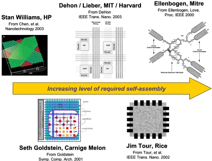
An example of the architectural variation in computational molecular electronics is shown in Figure 2, listed in order of the degree of self-assembly required. Hewlett Packard’s architecture, lead by Stan Williams, is based upon the “Teramac” computer7,20 which was developed in the mid 1990’s at Hewlett Packard21. It is an architecture based upon the crossbar-array structure, a commonly employed system in early computers, now being resurrected in molecular electronics22. The implementation proposed by Hewlett Packard requires only a single self-assembly step, using only one type of molecule (R(n) rotaxane) and one type of base material (platinum, gold or aluminum) to assemble upon20,23. The successfully written ASCII text string “HPinvent” into an 8x8 crossbar memory within a
Increasing level of required self-assembly
Stan Williams, HP
Seth Goldstein, Carnige Melon
Dehon / Lieber, MIT / Harvard
Jim Tour, Rice
Ellenbogen, Mitre
From Chen, et al. Nanotechnology 2003
From Tour, et al. IEEE Trans. Nano. 2002 From Goldstein
Symp. Comp. Arch. 2001
From DeHon IEEE Trans. Nano. 2003
From Ellenbogen, Love. Proc. IEEE 2000
Figure 2: Self-assembly required for various architectures
Earlier versions of this crossbar technology have been used to demonstrate electrically configurable wired-logic gates20, which will be used as cellular logic blocks in a Teramac-based architecture. Although the structures themselves contain little information
post-fabrication, a subsequent programming step would add information into the architecture through the use of lookup tables7,20.
technology node under production that year. This approach however, requires many levels of self-assembly to synthesize highly complex, post-fabrication information-containing structures, specific to a particular application. In addition, the chemical attachments of molecules that independently behave in one way, do not behave as devices in a simple series or parallel circuit, rather, as entirely new molecules26,27. Not surprisingly, no fully-molecular logic gates have been synthesized using this approach. Because of the difficultly in achieving multi-level self-assembly and the complexity of the required substrates, the architectures which have thus-far made the most experimental progress generally require only a low degree of self-assembly, contain very little information post-fabrication and utilize a post-fabrication programming step to add application-specific content.
2.2 Transport and Modeling of Devices
Since the first suggestion that molecular elements could be designed to control electronic properties in a circuit13, the vast majority of research in molecular electronics has focused on measuring and predicting electronic transport through organic devices. Organic materials of all types have been studied, including metallic and semiconducting carbon nanotubes28,29,30, silicon nanowires15, oligo(phenylene ethnylene) (OPE) based bistable molecular switches31,32, insulating alkanethiol chains33,56, slightly more conductive OPEs and oligo(phenylene vinylene)s (OPVs)44,49,55, and charge-storage molecular systems such as ferrocenes19. Understanding electron transport and charge storage is extremely important to advance the process of engineering molecules for specific applications41.
Where silicon device characteristics are engineered by varying the carrier density through doping techniques, designing molecular devices involves modifying electronic wavefunctions at a metal-molecule-metal junction26. However, as silicon devices continue to
fields of silicon nanoelectronics and molecular electronics, with each group leveraging off the knowledge created by the other.
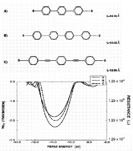
Most of the molecular electronic compounds listed above are only just a few angstroms to tens of angstroms in length. With only a few atoms involved in electron transfer, the notion of a density of states becomes less accurate and the properties of these molecules are better described by the location and energy gaps of their highest occupied molecular orbital (HOMO) and lowest unoccupied molecular orbital (LUMO) 34,57. With a few exceptions such as metallic and semiconducting carbon nanotubes26, it is expected that the Fermi levels of the metallic contacts will lie within the HOMO-LUMO gap of most molecules. This is illustrated in Figure 3, where the energy gap within most molecules34 is likely to be approximately 2-3 eV.
Figure 3: Metal-Molecule-Metal junction. From Samanta et al.34, "Electronic conduction through
organic molecules."
With this model, it is expected that the primary mode of electron transfer will be tunneling, rather than propagation14,26,33,34,57. A simple approximation for tunneling current
through a molecular junction can be modeled using the expression, kET = k0e-βd, where kET is
varying numbers of methylene groups), the current density (at a given voltage) across the junction will exponentially decrease as the molecular length increases. This is seen quite clearly in alkane chain conductivity research using mercury drop electrodes56, nanopores33 and STM analysis35. However comparing two structurally different molecules whose lengths are the same, research has shown that the tunneling currents can be very different49,55. This has lead to the belief that the parameter β can be used to describe the electron transmission properties of different molecules56.
Experimental research has shown that molecules exhibiting a highly π-conjugated
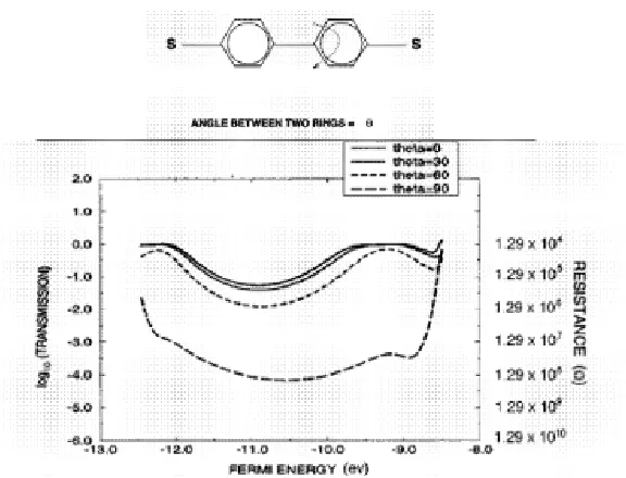
structure (such as OPEs and OPVs), as compared to the σ-bonded alkane chains, have a much lower gap resistance in metal-molecule-metal structures44,49,55. This suggests that the barrier to electron transfer is lowered within molecules containing delocalized electron clouds34,45. To more accurately account for scattering (which is neglected in the tunneling approximation) and the specific electronic structure for various molecules, many theorists use Density Functional and Green’s Function based approaches for more accurate evaluations34,36,3757. An example of the value in these approaches is shown in Figure 4, where the transmission properties for three different molecules were calculated and plotted. Samanta and Datta34 found that the resistance of a four benzene chain molecule scaled higher as expected when compared to a shorter, three benzene molecule. However, a three ring OPE was found to have a lower resistance than the four ring benzene chain, even though the OPE is a longer molecule. This was attributed to the presence of the triple bond in the OPE, causing a more delocalized electronic structure.
planar and exhibiting less bond-length alternation, were determined to have a slightly lower gap resistance.
Many have suggested using a third gate electrode to modulate transmission properties through a molecule25 by twisting or bending the molecular backbone, however concentrating a strong enough field in a gap less than 50 angstroms is extremely difficult. A theoretical study of a molecular three terminal device was performed by Datta38 at Purdue, using a single benzene ring as the conductive channel. To get good control of the channel, i.e., to get a high enough field to modulate the device, the equivalent gate oxide would need to be less than 10% of the channel length. This suggests that the gate electrode would need to be within two angstroms of the benzene ring, placed within an atomic level of accuracy. For these reasons, most research into molecular electronics has focused on two terminal devices, primarily switches.
Figure 4: Green-function analysis of electronic transmission through different molecules. From Samanta, et al.34, "Electronic conduction through organic molecules."
Figure 5: Ring orientation effects on the tranmission property. From Samanta, et al.34, "Electronic
conduction through organic molecules."
Figure 6: Suggested molecular electronic devices. From Joachim et al.26, "Electronics using
hybrid-molecular and mono-hybrid-molecular devices."
2.3 Device Characterization, Nanostructures and Test Beds
are often at or below 20 angstroms in length. As first suggested thirty years ago13, molecules could potentially be used to perform the same electrical functions that solid state devices perform today. Of course, to perform electrical functions there must be an electrical path. This requires molecular electrical characterization structures to bring into close proximity, with atomic precision, at least two metallic or semi-conducting probes through which external currents and voltages can be applied and measured. Furthermore, the effect of these contacts must be thoroughly understood and even decoupled from the device itself since they will inevitably alter the electronic properties of the molecules under investigation16,39,40.
Figure 7: Catagories of Molecular Test Structures. From Allera et al.16, “Evolution and Strategies for
Self-Assembly and Hookup of Molecular-Based Devices.”
2.3.1 Simple Molecular Self-Assembly
Structures that attempt to characterize single molecules or small groupings using fabricated or wired electrodes offer the potential to characterize the most basic elements proposed in molecular computing13,26. These structures have the unique capability of characterizing very small numbers of molecules in which both terminal junctions are created through self-assembly. Devices based upon these techniques offer perhaps the greatest physical certainty of fully-fabricated or wired test structures.
The most difficult challenge in creating these types of structures is the fabrication of a metal-space-metal junction, into which the molecules of interest can assemble. Since many of these molecules are often less than 100 angstroms in length14,16,41,42, the most obvious difficultly is the fabrication of gaps between proximal probes. Although electron-beam and nano-imprint lithography can pattern features into this link scale, their relative tolerances are far too great to be used as a platform for proximal probes in this application43. A second difficulty arises in the chemical assembly of single molecules into a fixed space. Although making longer molecules could reduce fabrication complexities, the more conductive, conjugated molecular wires exhibiting longer lengths and higher conductivity typically
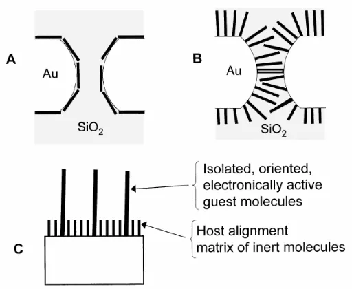
have a tendency to lie flat on the electrode surface rather than perpendicular across the probe gap. In addition, the longer the molecule, the greater this attractive force will be16, making electrical characterization of longer molecular wires potentially more difficult. One method, illustrated in Figure 8, involves first assembling a host matrix onto the metallic surface, then substituting the molecule of interest into this monolayer16,45. This method allows for a more consistent take-off angle, and also isolates the longer conjugated oligomers into single sites for easier analysis44,45 of individual molecules (further discussed in Section 2.3.4).
Figure 8: Orientation of molecules between two probes. From Allera et al.16, “Evolution and Strategies
for Self-Assembly and Hookup of Molecular-Based Devices.”
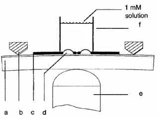
concentration of 1mM in tetrahydrofuran (THF). Shown in Figure 9 is the mechanically-controlled break junction (MCB).
Figure 9: Mechanically-controlled break junction (MCB). From Reed et al.46, “Conductance of a
Molecular Junction.”
Figure 10: Assembly and electrical data from the MCB. From Reed et al.46 "Conductance of a Molecular
Junction."
Although the data taken from this experiment are somewhat close to experimental data taken using other methods47, the structure itself raises several questions as to the nature
of the contact. Because the wire tips are formed through a mechanical stress and fracture process, the exact shape and geometry of the tips are unknown, providing uncertainty as to the exact number of molecules involved in the measurement. In addition, it is not know if both gold-sulfur junctions were formed through chemical assembly, if one was physically contacted, or if two molecules that each adsorbed onto a lead where brought into close proximity.
accurate interpretation of the device cross-sectional area, which directly relates to the number of molecules involved in transport measurements50.
Figure 11: Crossed wire tunnel junction. From Kushmerick et al.49, "Effect of Bond Length Alternation
in Molecular Wires"
Figure 12: OPEs investigated. From Kushmerick et al.48, "Metal-Molecule Contacts and Charge
Transport across Monomolecular Layers: Measurement and Theory"
Figure 13: Experimentally determined transport characteristics of OPEs. White symbols correspond to positive bias and black symbols to negative bias. The plot (a) is compound 1, and (b) is compound 2. From Kushmerick et al.48, "Metal-Molecule Contacts and Charge Transport across Monomolecular
Layers: Measurement and Theory"
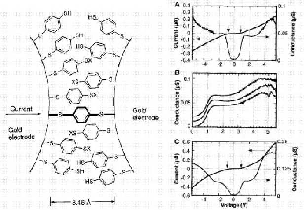
positive bias corresponds to electron injection at the Au-phenylene interface, suggesting a lower barrier than for the Au-S interface. This result bears similarity to previous work performed by Reed51 using a nanopore, where asymmetric contacts resulted in asymmetric rectification in DC bias sweeps, suggesting the Au-S interface presents a higher barrier than the evaporated top contact, where no sulfur linkage is present. Theoretical work has also suggested that the Au-S linkage, although well understood in the formation of self-assembled monolayers16, provides perhaps the worst electrical contacts between molecules and metals52. Kushmerick also demonstrated that theoretical modeling of the system using Green’s functions techniques and were in line with the results, although since the exact number of molecules involved in the system is unknown, only relative comparisons can be made.
In an attempt to further understand the nature of the contact area and to investigate the electrical properties in scaling from several to over a thousand OPEs in parallel, Kushmerick50 used the same crossed wire device and measured the I-V response as a function of deflection current. The OPE studied in this experiment was also a three phenyl-OPE, but contained an isonitrile (Au-CN) alligator clip only on one end.
Figure 14: I-V plotted as function of deflection current. From Kushmerick et al.50, "Conductance Scaling
of Molecular Wires in Parallel"
The initial I-V sweep indicated a rectifying, slightly asymmetric response, which was attributed to asymmetry in the contacts and endgroups. As the deflection current was increased, the I-V sweeps shifted uniformly towards a more conductive state. Based on the results of previous STM analysis53,54, it is suggested that the loading force’s affect on the contact area would serve to increase the area, effectively raising the junction conductivity. Kushmerick normalized each of the I-V sweeps by using an integer divisor, which resulted in the nicely overlapping curves shown in Figure 14. Knowing that Hertzian mechanics dictate that the contact area should scale as (load)2/3, Kushmerick showed that the integer divisors agreed with the expected load model for the lower forces, but disagreed for the higher contact forces. Although the higher forces could affect the electronic properties of the molecules in that region, that explanation was deemed unlikely because of the uniform similarity in all curves after normalization. It was noted that a similar deviation was observed in the previous STM work53,54, attributed to a change in charge transport. Most importantly, this work demonstrated that for larger contact areas involving hundreds of parallel molecules, the conductance of the junction scales linearly with area, which is in agreement with previous theoretical work performed by Magoga and Joachim27.
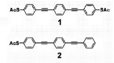
Since the nature of the contact region (in terms of shape and molecular attachment) is quite repeatable for this crossed-wire test structure, NRL experimentally compared the DC electrical response49 of three separate molecules with the response measured55 in an STM system. Compound 1 is a C12 alkane, compound 2 an OPE, and compound 3 an OPV, with each oligomer containing three phenyl groups. All of molecules measured were terminated at each end with thioacetyl groups for protection. In both experiments, it was determined
Another method for contacting a large number of molecules was developed at Harvard by Holmlin and Whitesides56. Liquid mercury was used as a top contact to a SAM formed, through sulfur linkages, to a gold surface. The motivation in using liquid mercury is to provide a top contact, on which sulfur chemistry can be performed, and whose application is gentle enough so as not to damage the SAMs under investigation. An example of a Au-C16//C16-Hg junction is shown in Figure 15.
Figure 15: Au-C16//C16-Hg junction. From Holmlin, et. al.56, "Electron Transport through Thin
Organic Films in Metal-Insulator-Metal Junctions Based on Self-Assembled Monolayers."
A SAM was formed on both the Hg electrode as well as the Au substrate to provide support and to prevent the coalescence of the mercury drop into the metal substrate. Holmlin’s experiments included varying the composition of SAM(1) while holding SAM(2) constant, as well as varying both SAM(1) and SAM(2) in order to keep the gap distance between the Hg and the Au identical. In all cases, the current density increased approximately linearly with respect to the contact area, which is in agreement with previous studies50,53,54. While holding one SAM constant, it was determined that the current flowing
I0e-βd, which is consistent with literature and is expected for a tunneling process57. While
varying both SAMs (each an alkanethiolate) but keeping the number of methylene groups constant between them, it was found that the difference in current densities was small compared to the first case where the gap distance was allowed to vary.
Although the liquid probe device offers a non-destructive method for establishing a top electrical contact to a SAM, the electrode material is restricted to metals which allow sulfur chemistry and also remain liquid at or near room temperature. In addition, the requirement for passivating the mercury probe itself with a SAM introduces the uncertainty of the SAM(1)//SAM(2) junction, which is likely to vary with the molecules and terminal groups of both SAMs. Finally, the size of the probe allows only larger-area contacts to be studied, eliminating the possibility for evaluating a range of contacts involving down to even a few tens of molecules. Nonetheless, the experiments provided several important comparisons between a variety of molecular systems, and help to strength the notion the direct tunneling is a large contributor to conductivity in many molecular systems.
Other approaches to fabricating small gaps have also been developed, which could be used for molecular characterization. One method involves forming nanometer-scale gaps in metallic wires using nanoimprint lithography and electromigration. Austin and Chou58 first patterned 20nm gold wires onto a insulating substrate, then passed a high DC current across the wire until a break formed. Using this method, gaps in the range of 10nm and some as small as 8nm were created. Of course, the exact location and geometry of the tip shape are uncontrollable. Another approach, developed by Morpurgo59 at Stanford, involves patterning a set of proximal probes, then plating gold onto these leads through electrodeposition. By monitoring the current passed between the wires, the system can be shut off when a gap of particular width has formed. Morpurgo used this technique to fabricate gaps of less then 20nm, however, the exact geometric shape of the tip is not controllable, and the metallic systems are limited to those which can be electrodeposited.
2.3.2 Object and Molecular Assembly
One way to reduce the atomic requirements on electrode gap distance is to use a multi-step approach, assembling the molecules on larger objects, and then joining these objects into larger features. One sacrifice made is the characterization of a single metal-molecule-metal junction, but certain properties can be derived using this hybrid approach in measuring several to many junctions at once.
In work done by Rawlett60 at Motorola, a series of proximal probes were fabricated in gold on a silicon dioxide surface, with gaps between 40 and 100nm. A drop of gold nanoparticles (ranging in size from 40nm to 120nm) suspended in water was placed on the substrate. An AC bias of less than 2.5V peak-peak, ranging from 1 to 10 MHz was used to dielectrophoretically trap the gold particles at the electrode tips, the location of the highest field gradient61. As shown in Figure 16, the smaller nanoparticles tended to clump together into larger groups, while the larger particles were trapped in fewer numbers. When first depositing a SAM of mononitrodithiol OPE on the electrodes, then trapping the molecules, the electrical data suggested increased conductivity and several regions of negative differential resistance.
Figure 16: Trapped colloids using dielectrophoresis. From Rawlett et al.60, "A molecular electronic
Although molecular junctions can be isolated and measured without the need for patterning atomic-scale gaps, the exact number and location of each junction cannot be controlled. Although post-measurement analysis could be used to confirm the number and location of nanoparticles, there is no way to isolate how many colloids are involved in electrical conduction. Further, the exact makeup of the Ted Pella, Inc. particles out of the vial is an unknown. A variety of materials could be bound to the surface of the gold colloids, including salts and species used for charge stabilization, and is likely in greater density for particles larger than 10nm in diameter62. The presence of these molecules brings into question the exact molecular makeup of each junction.
Rather than relying on dielectrophoresis to bring gold particles into a junction, Janes63 at Purdue chemically assembled a 2D network of 4nm gold nanoparticles, forming a hexagonal matrix on silicon dioxide. This matrix was formed on a surface containing proximal probes, separated by a distance of 500nm. Shown in Figure 17 is the matrix of gold nanoparticles, in a region between the electrical probes.
Figure 17: 2D matrix of 4nm gold particles. From Janes et al.63, "Electronic conduction through 2D
Dodecanethiol-encapsulated gold nanoparticles were allowed to assemble into a closed packed array, from solution, onto the substrate. Once assembled, the substrate was immersed into a solution containing the di-isonitrile molecule shown in Figure 18, approximately 22 angstroms in length. While in solution, the research suggests that a fraction of di-isonitrile molecules are substituted into the dodecanethiol molecules on the surface of the gold nanoparticles. The addition of these di-isonitrile OPE molecules should add to the conductivity measured at the electrodes. Electrical measurements agreed with this theory, showing a large drop in measured resistance between the two electrodes, from the as-deposited, dodecanethiol-encapsulated matrix.
Although this experiment does relatively agree with similar measurements taken on OPE based molecules48,49,55,44, the exact number of junctions involved in the current path is unknown, as well as the exact effect of the di-isonitrile OPE. No results from control experiments are presented, suggesting perhaps the organic solvent itself (or a part of that step) might have contributed to the increased conductivity. Nonetheless, the idea for cross-linking gold objects into a 2D matrix is one that other groups have suggested for more advanced molecular electronics architectures64.
Figure 18: Crosslinked 2D cluster electrical response. From Janes et al.63, "Electronic conduction
In work performed by Parker65 at Birmingham, Edgbaston in the United Kingdom, a solution of 2nm diameter dodecanethiol-passivated gold colloids, suspended in toluene, was dropped onto a prepatterned substrate. Substrates of both silicon and silicon dioxide (hydrophobic and hydrophilic respectively) were used, with a layer of patterned photoresist deposited on the surface. By allowing the toluene to evaporate then removing the resist with acetone, a patterned layer of gold nanoclusters was formed on both substrates. Other methods, using various silane binding chemistries66, have also been attempted in the deposition and patterning of gold colloids onto silicon dioxide surfaces, but similarly have not achieved the uniform, high density matrices needed for subsequent molecular attachment. An approach by Brown67 at Penn. State involved taking these less-dense colloid films, then reducing Au3+ electrolessly, causing the colloids to grow and the gaps to shrink. The gap sizes were reduced to approximately 10nm with this method, which offers the possibility to reduce gaps between isolated gold structures where electrodeposition is not possible.
Other methods including evaporation and sputtering have been used to create discontinuous gold films68,69,70,71,72 which have been studied for almost thirty years, primarily for their optical properties72. In a study by Harsdorff71 which focused on evaporation and r.f. sputter depositions, three types of condensation mechanisms were suggested: 1. layer by layer growth (van der Merwe), 2. nucleation then island growth (Volmer-Weber) and 3. adsorption then nucleation followed by growth (Stranski-Krastanov). The mechanism of growth depends upon the interaction between metal atoms and the binding strength of the atoms to the substrate. For gold on silicon dioxide, the gold-gold interactions are stronger than for gold-silicon dioxide, resulting in island growth by the Volmer-Webmer mechanism71. This growth mechanism has been studied for gold on a variety of substrates, including mica71, NaCl69,71, carbon71 and glasses68,70. The location, number of nucleation sites and size of the gold islands has been shown to depend upon the deposition method71,72, substrate material71, deposition rate71, deposition time68,69,72, temperature72, atmosphere70 and electric field73,74,75,76, among other variables.
island size and shape. For all temperatures studied, the particle sizes and fill factor increased as the sputtering time increased.
Figure 19: Gold clusters deposited at (a) 25oC, 3s (b) 160oC, 8s (c) 200oC, 8s (d) 250oC, 8s. From
Parmigiani et al.72, "Optical properties of sputtered gold clusters."
As seen in Figure 19, the islands all take on a colloidal shape, with exact size distribution and fill factor depending upon the deposition conditions. Also noted were differences in the characteristic absorption shift (due to surface plasmon resonance) as a function of deposition temperature. The shift in absorption towards red, seen as a function of fill factor at lower deposition temperatures, did not occur at higher temperature depositions, even as the fill factors increased over 20%.
including platinum78,79,80, silver81,82,83,84,85,86,87,88, copper86,87 and palladium81,87,88, introducing the possibility for studying various other metallic contact chemistries40. The study of palladium for these technologies is most promising due its expected low contact resistance when bound using sulfur chemistries40, and its refractory property allowing the conduction of higher current densities.
2.3.3 Physical Vapor Deposited Top Contact
Evaporating metal onto a self-assembled monolayer offers perhaps the easiest method for contacting a molecular device, but is also one of the most challenging methods studied. Defects in the monolayer serve as sites for shorts upon evaporation, and the impinging flux of metallic atoms during the evaporation process itself could damage or alter the organic film32,56,89.
One of the first studies of organic self-assembled monolayers using this type of junction was conducted by Zhou51 at Yale, using a structure they named the “nanopore.”
Figure 20: Nanopore. From Zhou et al.51, "Nanoscale metal/self-assembled monolayer/metal
heterostructures."
The contact area was defined by the nanopore, and kept small to minimize the chances that defects in the monolayer would be present in the junction itself. The titanium layer was chosen because of its known property to react with the organic layer39, suggested by Zhou to help form a better contact. Results from this experiment showed a strong rectification in the positive bias direction (electrons emitted from the Ti/Au), but virtually no rectification in the negative bias direction, swept between -5 and 5 volts. The cause of the rectification was suggested to result from the higher work function of gold than titanium, causing a lower barrier for electron injection from the bottom contact. Through extended temperature measurements, the transport mechanism was attributed to thermally activated injection of electrons under positive bias, and hopping conduction under negative bias.
deposition an unknown. Konstadinidis and Allara39 showed that titanium, when vapor deposited on alkanethiol SAMs with various end functional groups, completely consumed groups of COOCH3, OH and CH. In a later study by Hewlett-Packard89, it was found that
evaporation of Ti onto a monolayer containing a long alkane chain pointing upwards did react to some extent with the organic layer. The long alkane chain served as a barrier layer in the film, which was covalently linked to a quantum dot structure. Reflection-absorption infrared (RAIR) spectroscopy was used to determine that a number of the methylene groups had reacted with the Ti, but it was not possible to tell how many or in what ratio the groups were consumed. Although the use of an inert metal, such as gold or silver, reduces the possibility of a reaction between the monolayer and electrode, these metals have a tendency to penetrate further into the SAM resulting in more instances of shorting89.
Using the same structure, but with gold on both electrodes, Chen32 at Yale studied the electrical characteristics of a modified OPE molecule, containing a nitro and amine group attached to the center of three phenyl groups. Chen found a region of negative differential resistance in the positive bias sweep, a characteristic of resonant tunneling diodes that are useful in many circuit applications90,91,92. Although theoretical studies have attempted to explain the NDR behavior in this93 and other molecules94, the characteristic has not yet been attributed to any specific mechanism.
In a more recent study, Wang33 at Yale used the same nanopore to characterize electron transport through a series of alkanethiol SAMs. Using chains of varying lengths [CH3-(CH2)n-SH] coupled with temperature-dependent measurements, Wang was able to
show that the dominant transport mechanism is tunneling, with current densities decaying
exponentially with alkanethiol length, as expected14,26,34,57. Their calculated β constant of 0.79 agrees with other experiments used in measuring similar alkanethiol chains56.
assembled upon and the other evaporated still suggests the possibility of asymmetry in the devices. Nonetheless, several groups have employed evaporated top contacts into their architectures for more complex devices20,23.
2.3.4 STM Analysis
The Scanning Tunneling Microcopy (STM) has proved a valuable tool in the analysis of specific molecular junction and even isolated, individual molecules themselves26. Structure44, conductivity35,44,55 and electrical switching95,96 are among the properties investigated using this technique. Even before experiment results uncovered the prospect of molecular switches32, STM analysis was used to experimentally confirm that molecular structure and composition have an influence on conductivity, and that length alone (i.e. barrier width) is not the only factor. In a study by Bumm and Weiss44 in 1996, a molecular wire (4,4’-di(phenylene-ethynylene)-benzothioacetate), previously shown to assemble on gold by substitution42, was assembled into a matrix of dodecanethiol molecules. The matrix
Figure 21: Inserted molecular wire into an alkanethiol matrix. From Cygan et al.45, "Insertion,
Conductivity and Structures of Conjugated Organic Oligomers in Self-Assembled Alkanethiol Monolayers on Au{111}."
Figure 22: STM contacts to groupings of molecules. From Cui et al.35, "Reproducible Measurement of
Single-Molecule Conductivity."