Design and Implementation of Memory
Controller for Real Time Video Acquisition
using DDR3 SDRAM
Prof. Arun.S.Tigadi1, Padmashree. G 2, Hansraj Guhilot3
Professor, Dept. of ECE, K.L.E’s Dr. M. S. Sheshgiri College of Engineering and Technology, Belgaum, Karnataka,
India1
PG Student [VLSI], Dept. of ECE, K.L.E’s Dr. M. S. Sheshgiri College of Engineering and Technology, Belgaum,
Karnataka, India2
Principal, K. C. College of Engineering and Management Studies and Research, Thane, Maharashtra, India3
ABSTRACT: This Memory is an inevitable component of the electronic design. There has been dynamic progression
in the design of electronic system. The growth in the technology externalizes the need for systems operating at high speed. Hence there has been sequential progression in the development of the memory designs form basic structure RAM, then to DRAM further SDRAM, the generation of memory devices DDR, DDR2 and lately DDR3 SDRAM. It mainly aims the interaction of memory and processor. The video application system requires large bandwidth. Live video transfer requires a system operating at very high bandwidth to capture the data from the camera and store it. The project is implemented with Xilinx ML605 Virtex-6 hardware platform. The reconfigurable attribute of FPGA is advantageous. The controller design features an economic memory design. This proposed design involves designing the memory controller for DDR3 SDRAM with IP and designed The DDR3 is 3rd generation DDR memory. It has 8n pre-fetch. It is implemented with shared DIMM namely SODIMM referred as (Small Outline Dual Inline Memory Module) and the size smaller than DIMM. memory controller. The results can be are verified with simulation tool and real time display of the stored data.
KEYWORDS:DDR3 SDRAM, Web camera, UART, Xillinx, MATLAB, VERILOG, FSM.
I. INTRODUCTION
There is a dynamic change in the processor technology operating at a very high speed. The evolution in memory devices paved the way for devices operating at high bandwidth, low power. This advance has led to the usage of memory device in various multi-media applications such as Live-video transfer, Home-security, Home-Automation.
Live video transfer requires a system operating at very high bandwidth to capture the data from the camera and store it on to a platform, and at the back end involves the display of the intermediate result. FPGA provides a reconfigurable platform for the processing of data. It is more advantages because its design time is less. The need and increase in high performance system, led to advance in two dimensional memory of SDRAM as DDR (Double data rate), DDR2, DDR3.
Fig 1: DDR3 DRAM cell array and I/O buffer.
(Virtex-5 FXT) FPGA as development board for video output. The paper projects capture of the image/ video from camera with real time constraints. The system can perform real time analysis monitor and manage the real time data. [4].
The paper has helped us in understanding how video processing is implemented with block level detail and accessing MPMC with efficiency.
Yanolu, Qlanlon Zhang and An Tang presented a paper with title “FPGA implementation of video transmission system video transmission based on long term Evolution”. The development platform is Xilinx virtex-6 FPGA ML605. The design utilizes little hardware resources and transmits video data in bi-direction format perfectly. The designed based band link in ISE and programmed protocol stack in SDK. [5].
Lamjed Touil, Lilia Kechiche, Bouravri Ouni have presented a paper with title “Generic SOPC platform for video interface system MPMC controller”. The paper describes image and video processing using reconfigurable FPGA. Xilinx Virtex-5 development board is used. MPMC is an efficient technique for interfacing micro-blaze and key rapid devices to SDRAM. It used 8 port DDR SDRAM transmits data. It is used in real time video application and performs various functions such as cut video detection video zoom in and out. [3].
The paper helps to brief about how to process image and video data.
Sabhana Aqueel and Kavita Khare have published a paper with title “Design and implementation of DDR3 SDRAM controller for high performance”. Increase in device performance presents difficulty to handle memory devices. The paper mainly aims in DDR3 memory controller. The controller is split into two sections as initialization and secondly into command FSM. Initialization includes power up etc operations, command FSM operations, Read, write and refresh. This paper mainly describes the overall DDR3 SDRAM architecture. [1].
II. PROPOSED DESIGN FPGA BLOCK DIAGRAM
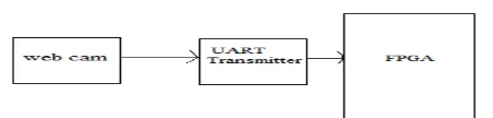
Fig 2: Block diagram for the real time data acquisition system.
The proposed design is implemented for real time video data acquisition system. The required interconnection with the system is established. The web camera captures, image and then send the data over UART. The frame of data is then transferred over UART communication protocol. The data is received by FPGA. The controller organizes the data storage efficiently. The bank0 is dedicated for the storage of the data in DDR3 SDRAM.
A.Web Camera:
Fig 3: Block diagram for capturing data through webcam.
The web-camera can be used to capture the video data. The web cam is plugged with USB cable or installed into computer hardware such as laptops etc. The resolution range is wide for different such as medium or high end web cam.
B.UART protocol:
UART is a serial communication protocol. UART converts the parallel data into serial format at the transmitter end and the serial received data into parallel format at the receiver end for the processing of data by host processor.
Fig 4: UART transmitter and receiver module.
In UART sender and the receiver don’t share same common clock. To avoid ambiguity sender and receiver are synchronized on a transfer-rate called baud rate.
Fig 5: UART data frame format.
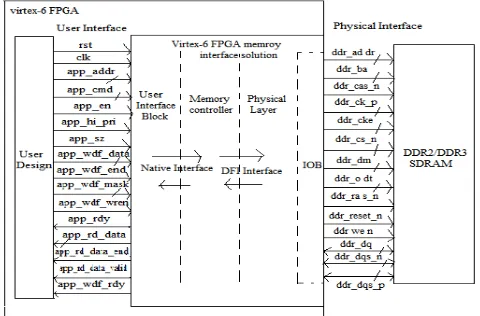
C. Memory controller design for DDR3 SDRAM with available:
The user design presents entire memory interface from the user end to the peripheral DDR3 SDRAM. User interface block is interfaced to the external DDR3 SDRAM. User interface is a measure to connect user design to memory controller. Memory controller is divided into two sections namely as first with front end of the memory controller, that involves providing a connection from native interface to UI.ead and write request by the user design are conceded by the native interface and also provides transfer of data from the user to external memory. The back end memory controller is employed by the interface at the physical end. The physical layer provides the necessary signals, timing comprising the clock, address, control logic, write, read and initialization of the memory devices. The physical layer does the power-up, Initialization of the memory and consecutive write leveling, write calibration, read phase detector calibration only after the reset function is disabled.
D. Designed DDR3 SDRAM controller:
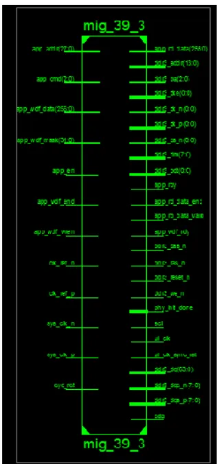
Fig 7: Internal block diagram of the Memory controller design.
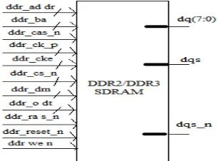
The signal ddr_ad_dr is of width 13 bits with width [12:0]. This involves the setting of the various parameters. Every position indicates some feature as described by MR0 (mode register) of the DDR3 SDRAM. The signal dq provides the data either to be read or written depending on operation. The dqs indicated the data strobe and it is bi-directional pin when the system is performing the write operation the controller issues the dqs command and vice versa in read command. The design involves initialization and followed by either read or write operation.
E. FSM for UART communication protocol:
Fig 8: FSM for UART protocol.
Firstly Start bit is generated, the data line( tx_reg) goes low when clock line is high then followed by sending the data bit frame with LSB data first and parity bit is generated if required and stop bit to stop the sequence and reload the transmitter if sending multiple bytes of data. Stop bit indicates the end of the sequence which is followed by pulling the data line (tx_reg) high when clock line is high.
The transfer is imitated by setting some parameters: 1. Baud rate.
2. Data frame format (5, 8 etc).
3. Parity option used and specify the type of parity either even or odd.
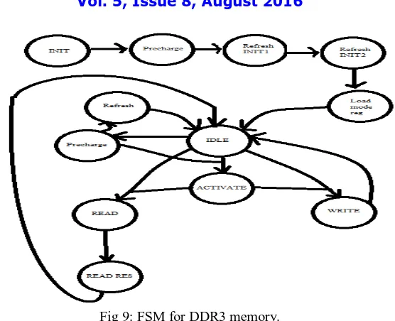
F. FSM for DDR3 memory:
Fig 9: FSM for DDR3 memory.
The memory controller design flow can be described as follows:
1. The DDR3 SDRAM memory is initialized with initialization signals prior to any communication to enable the information regarding the status of the signal.
2. After initialization, pre-charge initialization is issued to check and ensure that no row or entire bank is being used.
3. The pre-charge operations returns the bank to the idle state, the refresh is then enforced to perform the desired action.
4. Another refresh command as a backup option to avoid failure. 5. The mode register mr0 is defined at this stage.
6. The operations performed till now are part of the initialization sequences.
7. The design at the idle state is activate for the desired operation either in terms of read or write. 8. If write then the address where the data to be written or stored is been issued previously. Then the
state machine gets terminated by returning to the idle state.
9. If read operation is to be performed the desired data is read and after the action the process terminates by returning to idle state.
10. If any further action is to be performed then the, repeat pre-charge following refresh and the operation.
III. RESULTS and DISCUSSION
Fig 10: RTL schematic of with IP design.
Fig 11: RTL schematic of designed controller.
Fig 12: Technology schematic of designed controller.
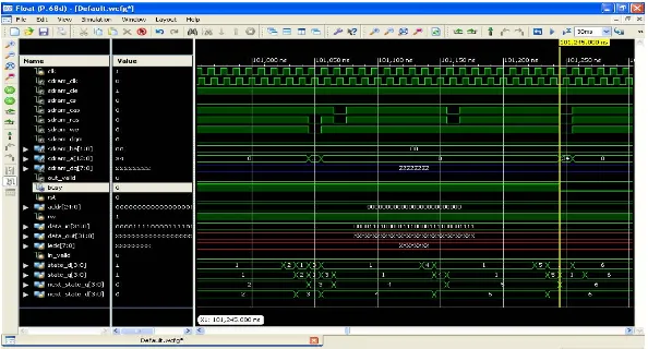
Figure 13, depicts the simulation result for the write operation for the designed system the change in state transition, starting from the initialization, bank selection, address and the desired write operation.
Fig 13: Simulation result of designed memory controller for write operation.
IV. CONCLUSION
This proposed system essentially features the design of the memory controller and implementation of the camera sensor for real time video with Xillinx ML-605(Virtex-6) FPGA. The camera captures the video data. The system is outlined to work at a frequency of 200MHZ. UART solely acts as the communication via between the camera module and the FPGA. The controller is employed with Xilinx ISE 14.6. The prototype developed can then be applied to numerous applications. The results are verified using real time display (VGA), ISM simulator. The project overviews the usage of ML605 and projects the efficiency of DDR3 SDRAM memory controller.
REFERENCES
[1] Shabana Aqueel and Kavita Khare, “Design and FPGA implementation of DDR3 SDRAM controller for high performance”, International Journal of computer science and Information technology.(IJCSIT) vol, No.4.,August 2011.
[4]. Sanjay Singh, Anil Saini, Ravi Saini, “Interfacing the Analog camera with FPGA Board for real time video acqusition”, I.J.image, Graphics and signal processing, 2014,4,32-38.(Modern Education and Computer Science(published online March 2014).
[5]. YanoLu, Qian Long Zhang and An Tang, “FPGA implementation of video transmission system based on LTE (Long Term Evaluation), MATEC web conference 22,91999(2015), published by EPD sciences 2015.
[6]. S.Jin, J.cho, X.D.Pham, K.M.Lee, S.k.Park, M.Kim and J.W.Jeon member IEEE, “FPGA design and implementation of Real time stereo vision system, IEEE Transactions on Circuits and Systems for video technology, vol.20.no.1, January 2011.
[7]. Zhenqian Shen, Chanyun Miao and Yan Zhang, “Memory Bandwidth Reduction for video decodes based on data arrangement”, 2013 6th
International Congress on Image and Spatial Processing(csip 2013), 978-1-4-799-2764-7/13, 2013 IEEE.
[8]. Taemin Lee, Dongki Kim, Hyunsun Park, Sungjoo Yoo, Sunggu Lee, “FPGA based prototyping systems for emerging memory technologies, 178-1-4795-6851-0/14, 2014 IEEE.
[9]. Radi, CalebW.W.K, M.N.Shah Zainudin, M,Muzafar Ismail, “The design and Implementation of VGA Controller on Fpga”, International Journal of Electrical and Computer sciences IJECS_IJENS vol:12.No:05.
[10]. Abhijith S, “FPGA based Multi Resolution Graphic Controller”, International Journal of Engineering Trends and Technology-volume 14 number6-aug 2014.
[11]. Xilinx, “Virtex-6 FPGA Memory Interface Solutions User Guide ug406”. [12]. Xilinx, ML605 MIG Design Creation.
[13]. DDR3 SDRAM specification(JESd7-9-3c) JEDEC standard, JEDEC Solid State Association, November 2008. [14]. UART( HTTP://EN.WIKIPEDIA.ORG/WIKI/ Universal Asynchronous Receiver Transmitter.
[15]. Kamal Kumar Sharma and Parul Sharma “FPGA-based implementation of UART” IJITKMI Volume 6 • Number 2 • July-December 2013 pp.-165-170.