International Research Journal of Engineering and Technology (IRJET)
e-ISSN: 2395 -0056 p-ISSN: 2395-0072 Volume: 04 Issue: 04 | Apr -2017 www.irjet.netSHIFT REGISTER USING CNT FET BASED ON SENSE AMPLIFIER
PULSED LATCH FOR LOW POWER APPLICATION
Muthusuriya.M
1, Shantha Devi.P
2, Poongodi.M
3Gayathiri.G
41PG Scholar, Department of ECE, Theni Kammavar Sangam College of Technology, Theni, Tamilnadu, India.
2PG Scholar, Department of ECE, Theni Kammavar Sangam College of Technology, Theni, Tamilnadu, India.
3PG Scholar, Department of ECE, Theni Kammavar Sangam College of Technology, Theni, Tamilnadu, India. 4Assistant Professor, Department of ECE, Theni Kammavar Sangam College of Technology, Theni, Tamilnadu.India.
---***---
Abstract
- Recent day’s power consumption and areareduction is the major concern in circuit design. Shift register is a basic building block of memory devices. In this design reducing power in shift register using pulsed latchesinstead of flip-flops. Because shift register based flip-flops consumemore power. The pulsed latches designed by Carbon Nano Tube technology. CNTFET technology is one of the best replacement of CMOS technology because of its excellent properties such as high thermal conductivity, small atomic diameter of carbon and also high tensile strength. Here shift register based on pulsed latches using CMOS technology and CNTFETtechnology has been compared. This shift register has been implemented in 32nm CNTFET technology in HSPICE.
Key Words: Pulsed latch, Shift register, Flip-flop, CNTFET memory devics.
1.
INTRODUCTION
In the past area, speed, and cost is the major concerns of the VLSI designers. Power consideration is the second concerned. Now a day’s power is the primary concerneddue to remarkable growth and success in the field of batteries based devices such as laptops, mobile phones, tablets etc. The motivations for reducing power consumption differ application to application.
There are different power minimization techniques are available. In a circuit three components are responsible for power dissipation: short circuit power, dynamic power and static power. Dynamic power is primary power dissipated when charging and discharging capacitors.
Pdynamic = CL VDD2 α f … (1)
Shift registers are a sequential logic circuit. It is used to shifting the binary information and also canstorethatbinary information. So only shift registers are basic building blocks in memory devices.
The following sections includes conventional shift register, shift register using pulsed latch, shift register based pulsed latch using CNTFET are discussed.
2.
LITERATURE SURVEY
International Research Journal of Engineering and Technology (IRJET)
e-ISSN: 2395 -0056 p-ISSN: 2395-0072 Volume: 04 Issue: 04 | Apr -2017 www.irjet.neteffective channel length CMOS. Umiing KO, et al., (1996) [8] presented performance, power, and energy efficiency of several CMOS master slave D flip flops (DFF’s). To improve performance and energy efficiency, a push pull DFF and a push pull isolation DFF are proposed. Among the five DFF’s compared, the proposed push pull isolation circuit is found to be the fastest with the best energy efficiency.
3.CONVENTIONAL SHIFT REGISTER
The Shift registers are normally having group of flip-flops. Flip-flop is a 1 bit memory cell. In shift register the flip-flops are controlled by the clock. The number of flip-flops in shift register represent the number of bits used in it. When clock pulse is high data bit is enter into the first flip-flop in the shift register and the data is shifted to the other flip-flop during each clock pulse. The shifting is done by two ways, one is serial shifting and another one is parallel shifting. The following fig.1 shows the master slave flip-flop and based shift register.
Fig-1: Master-slave flip-flop.
The following fig.2 represent the one of the flip-flop model namely Power PC Style flip-flop (PPCFF). It is fastest and high quality structure and have a short direct path and low power clock load.
Fig-2: Schematic diagram of PPCFF.
An optimized shift registers are not designed by flip-flops because it consume more power and impose heavily clock load.
4.
SHIFT REGISTER USING PULSED LATCH
4.1.
Pulsed latch
The important parameters of shift register such as area, power and delay can be reduced by the use of pulsed latch. Pulsed latch means that combination of latch and pulsed clock generator. The fig.3 represent the pulsed latch circuit. Pulsed latch have small number of transistors compare with flip-flop. So the area of the shift register will become reduce. Pulsed latch is a latch that can capture the data during the particular time defined by the width of clock waveform. Pulsed latch uses narrow clock pulse so important low power characteristics such as clock power will be low.
Fig-3: Pulsed latch circuit.
This shift register solves the timing problem between the latches by the use of multiple non overlap delayed pulsed clock signals. The pulsed clock generator generates the pulsed clock signals. Another one advantage of the pulsed latch is to reduce the hold time violations. Because pulsed latch is an ideal sequential component for high performance and low power VLSI design environment.
4.2.
Pulse clock
generator
Pulse clock signal generated in a pulse clock generator consisting of delay circuits and AND gate. The clock pulse width in the conventional pulse clock generator is larger than the summation of rising and falling times. But delayed pulsed clock generator produces pulse width is smaller than the summation of rising time and falling times.
Fig-4: Pulsed clock generator.
International Research Journal of Engineering and Technology (IRJET)
e-ISSN: 2395 -0056 p-ISSN: 2395-0072 Volume: 04 Issue: 04 | Apr -2017 www.irjet.net4.3.
Sense amplifier pulsed latch
[image:3.596.311.498.104.291.2]In this shift register based pulsed latch design, we select the one of the pulsed latch type is static differential sense amplifier shared pulsed latch (SSASPL). Because the short clock signal used in shift register cannot through the long wire due to the parasitic capacitance and resistance. The clock pulse shape is degraded at the end of wire because rising and falling times of clock pulse increases due to wire delay. One way to solve this problem by increase the clock pulse width but this makes decrease the clock frequency. Final solution of this problem is inserting the clockbufferfor send the clock pulse with small wire delay. The following figure shows the schematic diagram of SSASPL. It has small number of transistors (9) compare with otherpulsedlatches.
Fig-5: Sense Amplifier Pulsed Latch.
4.4.
Shift register based SSASPL
[image:3.596.48.233.289.420.2]The proposed shift register consisting of sense amplifier pulsed latch. The N bit shift register divided into M bit sub shift register. N bit shift register have N+1 latches because N latches for N bit and one for temporary latch is used for temporary storage the bit for next latch in next shift register. Dividing the N bit shift register is used to reduce the delayed pulse clock signals. Each shift register performs shifting operations with N+1 latches. This shift register solves the timing problem between the latches by using multiple non- overlap delayed pulsed clock signals instead of single pulsed clock signal. The following diagram the shift register using SSASPL.
Fig-6: Shift register using SSASPL.
5.
SHIFT REGISTER USING CNTFET
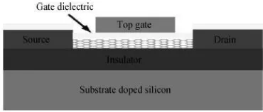
Carbon Nano Tube is a carbon allotropic variety, tubeshaped material and having a diameter measuring onthenanometer scale. It was discovered by Ijima in 1991. CNT is a suitable alternative to conventional silicon technology for future nano electronics because of their unique electrical and mechanical properties. Also has 1D ballistic transport of electrons and holes. Carbon Nano Tube Field Effect Transistor is a transistor that employs the single CNT or array of CNTs as a channel material instead of polysilicon in the conventional MOSFETs. CNTs play a role onbothsideson thermal insulation due to unique in that they are thermally conductive only along their length not sides of it. The important parameter of the CNT is chirality that means the distortion or direction to rolled by the grapheme. Carbon nano tubes are high strength and less weight material and flexibility allow for them to be added other materials. The structure of the CNTFET is same as the MOSFET except the CNT is attached between the source and drain then act as a channel.
Fig-7: Schematic diagram of CNTFET.
[image:3.596.341.526.592.671.2]International Research Journal of Engineering and Technology (IRJET)
e-ISSN: 2395 -0056 p-ISSN: 2395-0072 Volume: 04 Issue: 04 | Apr -2017 www.irjet.netFig-8: Rolled up sheet of grapheme.
The sense amplifier pulsed latch is used in the shift register. It requires pulsed clock signal and two differential inputs. It requires 17 transistors in which M1-M10 transistors are used to generate the pulsed clock signal. The remaining transistors M11-M17 represent the sense amplifier pulsed latch operations. Here 4 bit shift register is considered. Usually shift register classified into four types as following, serial in serial out (SISO), serial in parallel out (SISO), parallel in serial out (PISO), parallel in parallel out (PIPO). The following figure represents the proposed shift register based pulsed latch using CNTFET. It has three connectionfor data shifting operations. The proposed shift register containing five pulsed latch serially. The data enter into the one latch, the output from that latch is connected to the next latch. The additional latch in the shift register isusedtostore the data temporally then send to the next latch in the next shift register. The first type is serial in serial out shift register (SISO) which accepts the data serially and produces data on output serially. The following diagram represents the serial in serial out shift register using CNTFET.
Fig-9: Schematic diagram of SSASPL using CNTFET.
Fig-10: Serial in serial output shift register using CNTFET.
6.
SIMULATION AND RESULTS
This section includes simulation of shift register using flip- flop, pulsed latch. The shift register using PPCFF simulation as shown in fig.
Fig-11: Shift register using PPCFF.
International Research Journal of Engineering and Technology (IRJET)
e-ISSN: 2395 -0056 p-ISSN: 2395-0072 Volume: 04 Issue: 04 | Apr -2017 www.irjet.netFig-12: Waveform of pulse clock generator.
The output of the pulsed clock generator is send to the input of the one NMOS transistor in SSASPL. The waveform of the SSASPL is as shown in fig.
Fig-13: Waveform of the SSASPL.
Finally, the output of shift register based pulsed latch using CNTFET technology is as shown in fig.
Fig-14: Waveform of shift register based pulsed latch using CNTFET.
And also compare the power delay product of PPCFF and SSASPL based shift registers.
C hart-1: Delay,power and powerr delay product(PDP) comparison of two shift register.
The following table represents the transistors comparison between the pulsed latches and flip-flops.
Table-1.Transistors comparison.
Type Number of Transistors
Sense amplifier pulsed latch
Transmission gate pulsed latch 10
Hybrid latch flip-flop 14
Power PC style flip- flop 16
Strong ARM flip-flop 18
Data mapping flip-flop 22
International Research Journal of Engineering and Technology (IRJET)
e-ISSN: 2395 -0056 p-ISSN: 2395-0072 Volume: 04 Issue: 04 | Apr -2017 www.irjet.net7.
CONCLUSIONS
This paper proposed the low power sense amplifier pulsed latch based shift register using CNTFET technology. Through the discussion we can conclude CNTFET is best replacement of MOSFET due to their power dissipation and delay.
REFERENCES
[1] Byung-Do Yang,” Low Power and Area Efficient Shift Register Using Pulsed Latchs”, IEEETransactionson circuits and systems I; regular paper, vol.62, no.6, June 2015.
[2] E. Consoli, M. Alioto, G. Palumbo, and J. Rabaey, “Conditional push-pull pulsed latch with 726 fJops energy delay product in 65 nm CMOS,” in IEEE Int. Solid-State Circuits Conf. (ISSCC) Dig. Tech. Paper Feb. 2012, pp. 482–483.
[3] S. Heo, R. Krashinsky, and K. Asanovic, “Activity- sensitive flip-flop and latch selection for reduced energy,” IEEE Trans. Very Large Scale Integr. (VLSI) Syst., vol. 15, no. 9, pp. 1060–1064, Sep. 2007. [4] P. Reyes, P. Reviriego, J. A. Maestro, and O. Ruano,
“New protection techniques against SEUs for moving average filters in a radiation environment,” IEEE Trans. Nucl. Sci., vol. 54, no. 4, pp. 957–964, Aug. 2007.
[5] B.-S. Kong, S.-S. Kim, and Y.-H. Jun, “Conditional- capture flip-flop for statistical power reduction,” IEEE J. Solid-State Circuits, vol. 36, pp. 1263–1271, Aug. 2001.
[6] Stojanovicand V. Oklobdzija, “Comparative analysis of master slave latches and flip-flops for high- performance and low-power systems,” IEEEJ. Solid- State Circuits, vol. 34, no. 4, pp. 536–548, Apr. 1999. [7] H. Partovi et al., “Flow-through latch and edge-
triggered flip-flop hybrid elements,” IEEE Int. Solid- State circuits Conf. (ISSCC) Dig. Tech. Papers, pp. 138–139, Feb. 1996.
[8] J. Montanaro et al., “A 160-MHz, 32-b, 0.5-W CMOS RISC microprocessor,” IEEE J. Solid-State Circuits, vol. 31, no. 11, pp. 1703–1714, Nov. 1996.
[9] C. K. Teh, T. Fujita, H. Hara, and M. Hamada, “A 77% energy-saving 22-transistor single-phase-clocking D-flip-flop with adaptive-coupling configuration in 40 nm CMOS,” in IEEE Int. Solid-State circuits Conf. (ISSCC) Dig. Tech. Papers, Feb. 2011, pp. 338–339. [10] H.-S. Kim, J.-H. Yang, S.-H. Park, S.-T. Ryu, and G.-H. Cho, “A 10-bit column-driver IC with parasitic- insensitive iterative charge-sharing based capacitor-string interpolation for mobile active- matrix LCDs,”IEEE J. Solid-State Circuits, vol., no. 3, pp. 766–782, Mar. 2014.
[11] Sanjeet kumar Sinha and Saruabh chadhury,”Comparative study of leakage power in CNTFET over MOSFET device,” Journal of semiconductors, vol.35, No.11, November 2014.
[12] U. KO and P. T. Balsara, “High Performance,Energy Efficient, Master-Slave Flip-flop Circuits,”