Design of Efficient Low Power Stable 4-Bit Memory Cell
K. Gavaskar
Assistant professor/ECE, Kongu Engineering College,
Erode, India
S. Priya
Assistant professor/ECE, Bannari Amman Institute of Technology
Sathyamangalam, India
ABSTRACT
The power consumption and speed of SRAMs are important issue that has led to multiple designs with the purpose of minimizing the power consumption during both read and write operations. Memory is the furthermost collective part in CMOS IC’s applications. Here a novel 9T static random access memory (SRAM) cell design which consumes less dynamic power and has high read stability is predicted. This paper also includes the SRAM array structure, it consist of sense amplifier and address decoders. The Tanner EDA tool is used for observe the schematic solution at different technologies. Based on the results obtained when compared with the existing methods, by utilizing the above proposed method it is clearly observed that there is a decrease in power consumption and stability improvement of the memory cells.
Keywords
Memory circuits, SRAM, Read and Write, Stack tech, Array.
1. INTRODUCTION
A SRAM cell involves of a latch, therefore the cell data is kept as long as power is turned on and refresh operation is not compulsory for the SRAM cell. SRAM is mainly used for the cache memory in microprocessors, mainframe computers, engineering workstations and memory in hand held devices due to high speed and low power consumption. For nearly 40 years CMOS devices have been scaled down in order to achieve higher speed, performance and lower power consumption. Technology scaling results in a significant increase in leakage current of CMOS devices. Static Random Access Memory (SRAM) continues to be one of the most fundamental and vitally important memory technologies today.
Each bit in an SRAM is stored on four transistors that form two cross-coupled inverters. High-performance on chip caches is a crucial component in the memory hierarchy of modern computing systems. In this technique each NMOS and PMOS transistor in the logic gates is split into two transistors are called Stack Technique [7]. Leakage current flowing through the NMOS transistor stack reduces due to the increase in the source to substrate voltage in the top NMOS transistor and also due to an enlarge in the drain to source voltage in the bottom NMOS transistor. The proposed SRAM memory cell consumes lower power during read and writes operations compared to 6T conventional circuit. The ability of the cell to write properly and to have sufficient read noise margin is very important for sub threshold region. Also, a new 9T SRAM combining the advantages of these circuits is proposed in the paper. A nine transistors (9T) SRAM cell configuration is proposed in this paper, which is amenable to small feature sizes encountered in the deep sub-micron/Nano CMOS ranges. Compared with the 8T and 10T cells of [1] and [2], the 9T scheme offers significant advantages in terms of power consumption. The conventional six transistor (6T) SRAM cell shows poor stability at very small feature size with low power supply. During the read operation, voltage
division between the access and driver transistors grounds the read stability to be very low. Hence in this paper, a 9T SRAM cell is proposed for high read stability and low power consumption. The proposed cell utilizes single bit-line (BL) for write operation, resulting in saving of dynamic power consumption. During read operation, the data storage nodes are completely isolated from the bit lines, thus patterned the read static noise margin. Hence in this paper, a 9T SRAM cell is proposed for high read stability and low power consumption [5]. The proposed cell utilizes single bit-line (BL) for write operation, resulting in reduction of dynamic power consumption. During read operation, the data’s are completely isolated from the bit line during read operation, thus improving the read static noise margin.
2. SRAM MEMORY CELL DESIGNS
2.1 Conventional 6T SRAM
SRAMs are a form of storage cells in which a bit is stored on a pair of cross-coupled inverters. Transistors (PMOS_1, PMOS_2, NMOS_1 and NMOS_2) act as the cross-coupled inverters, while transistors NMOS_3 and NMOS_4 act as access transistors to allow reading and writing. The word line (WL) is used to activate the access transistors during read and write operations whereas the bit lines are used to read/write a value from/to the cell. Since an SRAM cell does not exist on its own but typically integrated in an SRAM array, the word line is shared among cells in the same row whereas the bit lines are shared by cells in the same column.
Fig1: conventional 6T SRAM cell
10 its inverse are typically provided since it improves noise
margins [11].
The read operation surprises by precharging the bit lines to VDD, then the access transistors are released by setting the word line and permitting the sense amplifier. Assuming grasps a zero, the access transistor NMOS_4 enters the saturation region and ejections the bit line through the transistor NMOS_1. On the other hand the access transistor NMOS_3 is in the sub threshold region and allows no current to pass, thus maintaining the voltage on the other bit line. The sense amplifier would then detect the difference between the voltages on the two bit lines and discharge quickly in order to read and protect the value saved within the cell.
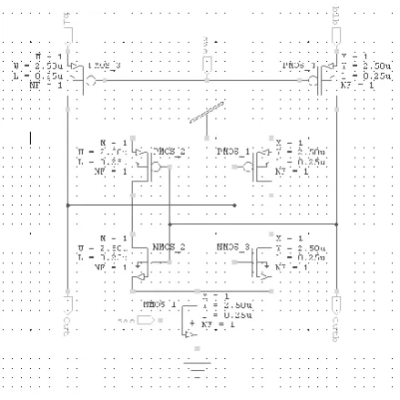
[image:2.595.320.542.189.370.2]2.2 Schematic 9T SRAM
Fig 2: schematic 9T SRAM cell
Schematic of 9T SRAM cell is shown in the Fig. 2. This circuit shows reduced leakage power and enhanced data stability. The 9T SRAM cell completely isolates the data from the bit lines during a read operation. The idle 9T SRAM cells are placed into a super cutoff sleep mode, thereby reducing the leakage power consumption as compared to the standard 6T SRAM cells.
2.3 Stack 9T SRAM
[image:2.595.67.270.242.416.2]Power consumption has become a critical design concern for many VLSI systems [12]. Leakage current flowing through the NMOS transistor stack reduces due to the increase in the source to substrate voltage in the top NMOS transistor and also due to an increase in the drain to source voltage in the bottom NMOS transistor.
Fig 4: stack technique
This reduces the power dissipation in logic circuits. In this technique each NMOS and PMOS transistor in the logic gates are split into two transistors. A state with more than one transistor is off condition from a path from supply voltage to ground path consist of less leakage equated to the only one transistor off condition from a path from supply voltage to ground path.
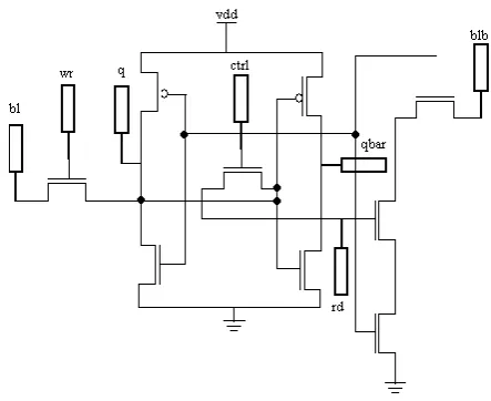
[image:2.595.70.269.586.725.2]2.4 Proposed 9T SRAM
Fig 6: proposed design
Here only one single bit line capacitance (BL) will be charged and discharged during write operation which results in important reduction in dynamic power consumption and at the equal time the data stability of the 9T SRAM [12] cell as in is also maintained. The planned cell maintains greatly improved write margins and functionality, even when the PMOS are much stronger than the NMOS ones. This cell completes full functionality deep into the sub-threshold section without the need for special peripheral circuits and techniques that necessitate additional power die area and timing schemes [6]. The optimum transistor sizing for this 9T SRAM cell considering stability, energy consumption and delay. A write bit line balancing scheme is proposed to reduce the leakage current of the SRAM cell. In this proposed SRAM cell single bit line capacitance will be charged and discharged, which results in possible amount of power should be reduced. By using stack effect the significant amount of leakage current should be reduced. A 9T structure is to improve the SNM by separating the read access structures of the original 6T cell, thus making the read SNM equal to the hold SNM. In addition, this circuit presents a low-leakage state, at which its static power is lower than any of the other enactments when operated at a similar supply voltage [3]. This is accomplished lacking any performance degradation, while keeping a reasonable SNM.
3. PROPOSED MEMORY ARRAY
3.1 Design of Sense Amplifier
[image:3.595.321.538.69.293.2]The sense amplifiers have to amplify the data which is present on the bit lines during the read operation. The memory cells are weak due to their small size, and hence cannot discharge the bit lines fast enough. Also, the bit lines continue to slew till a large differential voltage is formed between them. This causes significant power dissipation since the bit lines have large capacitances. It consists of two cross coupled gain stages which are enabled by the sense clock signal. The cross coupled stage ensures a full amplification of the input signal. This type of amplifier consumes least amount of power. If the sense amplifiers enabled before sufficient differential voltage is formed, it could lead to a wrong output. Thus, the timing of the sense clock signal needs to be such that the sense amplifier can operate over various process corners and temperature ranges. The latch based sense amplifier consumes less power when compared with other types of sense amplifiers to enhance the data stability.
Fig 7: sense amplifier
3.2 Decoder Design
[image:3.595.58.278.280.500.2]Usually the memory address decoder is divided into two parts, row decoder and column decoder. If the address bits of the memory are m bits, there are m1 bits for the row decoder and m2 bits for the column decoder (m1+m2=m). The column decoder should select the corresponding bit line of the desired memory cell design. The row decoder should select the corresponding word line of the desired memory cell design.
Fig 8: decoder design
3.3 Design of SRAM Array
The SRAM array structure [10] consists of SRAM memory cell, row and column decoder, sense amplifier. The row decoder and column decoder are used to select the particular cell onto which the data is to be written or from which the data is to be read. In our simulation, we designed 4X4 array. The schematic of the SRAM array is as shown below.
[image:3.595.321.539.393.703.2]12
4. SIMULATION AND ANALYSIS
4.1 Simulation Result
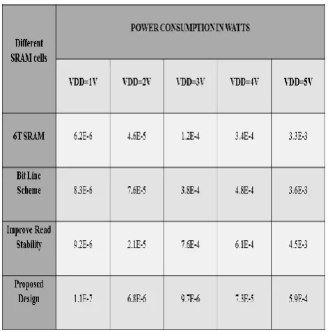
All the circuits have been simulated using BSIM 3V3 125nm, 45nm and 180nm technology on Tanner EDA tool with supply voltage ranging. The maximum operating frequency of the SRAM cell is 165 MHZ. The power results values are calculated at different supply voltages and frequency. In our proposed array design consume less power compared to design a SRAM array with 6T SRAM cell.
[image:4.595.316.549.84.273.2]Table 1. Power comparison at 45nm technology
[image:4.595.54.290.201.440.2]Table 2. Power comparison at 250nm technology
Table 3. Power comparison at 180nm technology
Table 4. Power comparison at different Vth
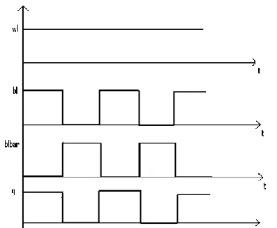
[image:4.595.318.547.298.473.2] [image:4.595.55.289.481.706.2]Fig 10: waveform for read/write operation of SRAM array
5. CONCLUSION
The proposed memory cell is accessible in this paper for high read stability and low enthusiastic power consumption. For low leakage and high speed circuits concern should be on both the factors such as speed and power. During the write operation, the SRAM cell utilizes the charging/discharging of only one bit line (BL), resulting in reduction of dynamic power consumption as compared to conventional 6T SRAM cell. Different techniques have been analyzed to reduce the standby leakage current and dynamic power dissipation of the SRAM cell. In the proposed method 45nm and 250nm and 180nm technologies are analyzed using the Tanner EDA software and is used to analyze parameters such as power consumption, delay time and operating frequency. Based on the results obtained when compared with the existing methods, by utilizing the above proposed method it is clearly observed that there is a decrease in power consumption and stability improvement of the memory cells.
6. REFERENCES
[1] Agarwal, K. and Nassif, S. (2006), “Statistical Analysis of SRAM Stability”, Proceedings of 43rd Annual Conference on Design Automation, 57.
[2] Agarwal, K. and Nassif, S. (2008), “The Impact of Random Device Variations on SRAM Cell Stability in Sub-90-nm CMOS Technologies”, IEEE Transactions on Very Large Scale Integration (VLSI) Systems, 16, 1, 8697.
[3] Bhavnagarwala, A.J., Tang, X., and Meindl, J. (2001), “The Simpact of Intrinsic Device Fluctuations on CMOS SRAM Cell Stability”, IEEE Journal of Solid State Circuits, 36, 4, 658-665.
[4] Bharadwaj, S., Amrutur and Mark, Horowitz, A. (2001), “Fast Low-Power Decoders for RAMs”, IEEE Journal of Solid-State Circuits, 36, 1506-1515, 10.
[5] Borkar, S., Karnik, T., Narendra, S., schanz, J.T., Keshavarzi, A. and de, V. (2003), “Parameter Variations and Impact on Circuits & Micro architecture,” Proceedings of Design Automation Conference., 338-342.
[6] Chang, L., Montoye, R.K., Nakamura, Y., Batson, K.A., Eickemeyer, R.J., Dennard, R.H., Haensch, W. and Jamsek, D. (2008), “An 8T SRAM for Variability Tolerance and Low-Voltage Operation in High-Performance Caches”, IEEE Journal of Solid State Circuits, 43, 4, 956963.
[7] S. Lin, Y.B. Kim, and F. Lombardi, \A Highly Stable Nanometer Memory for Low-Power Design," Proceeding of IEEE International Workshop on Design and Test of Nano Devices, Circuits and Systems, pp. 17-20, 2008.
[8] Dandapat, A., Kayal, D., and Mukhopadhyay, D. (2008), “Design of a Low Leakage, Low Power and High Performance Search and Read Memory using CAM and SRAM”, Journal of Low Power Electronics, 4, 1–11.
[9] ESeevinck, S., List, F.J. and Lohstroh, J. (1987), “Static Noise Margin Analysis of MOS SRAM cells”, IEEE Journal of Solid State Circuits, 22, 5, 748-754.
[10]Jan, M., Rabaey, Anantha Chandrakasan and Borivoje Nikolic (2003),”Digital Integrated Circuits”, ISBN 81-7808-991-2.
[11]Liu, Z. and Kursun, V (2008), “Characterization of a Novel Nine-Transistor SRAM Cell”, IEEE Transactions on Very Large Scale Integration (VLSI) Systems, 16, 4, 488-492.