N A N O E X P R E S S
Open Access
Current Rectification in a Structure: ReSe
2
/
Au Contacts on Both Sides of ReSe
2
Tingting Miao
1†, Dongwei Yu
2†, Lei Xing
3†, Dawei Li
1, Liying Jiao
3, Weigang Ma
2*and Xing Zhang
2Abstract
Schottky effect of two-dimensional materials is important for nanoscale electrics. A ReSe2flake is transferred to be suspended between an Au sink and an Au nanofilm. This device is initially designed to measure the transport properties of the ReSe2flake. However, a rectification behavior is observed in the experiment from 273 to 340 K. The rectification coefficient is about 10. The microstructure and elements composition are systematically analyzed. The ReSe2 flake and the Au film are found to be in contact with the Si substrate from the scanning electron microscope image in slant view of 45°. The ReSe2/Si and Si/Au contacts are p-n heterojunction and Schottky contacts. Asymmetry of both contacts results in the rectification behavior. The prediction based on the thermionic emission theory agrees well with experimental data.
Keywords:ReSe2, Rectification, Two-dimensional materials
Introduction
Rectification behaviors of metal-semiconductor contacts, where the current varies with the direction of the applied voltage, are widely used in Schottky barrier diode, field ef-fect transistor (FET), and metal-oxide-semiconductor FET. Schottky explained the behavior by depletion layers on the semiconductor side of such interfaces [1]. Differ-ences of electron work function between metal and semi-conductor lead to the rectification behavior named Schottky effect [2]. The contact between metal and two-dimensional (2D) semiconductor materials is a Schottky contact when the metal has a higher electron work function than an n-type 2D semiconductor materials or lower electron work function than a p-type 2D semi-conductor. The Schottky effect of metal/2D materials has great applications in micro-photo detectors, micro-FETs, gas sensors, and phototransistors [3]. Among 2D mate-rials, transition metal dichalcogenides (TMDs) have attracted much attention because they have a sizable bandgap [3] and the bandgap transits from indirect to dir-ect as the thickness is reduced to monolayer [4]. The bandgap ensures that TMDs can be used for many
applications, i.e., FETs and solar cells [3]. TMDs can be also used in thermoelectric field [5], which has drawn wide attention [6–9]. Many experiments have been done to explore properties and applications of TMDs such as MoS2, MoSe2, WSe2, and WS2. Lopez-Sanchez et al. [10] made ultrasensitive monolayer phototransistors with MoS2. Britnell et al. [11] made a WS2/graphene hetero-structure and demonstrated its application in photovoltaic device. WSe2, as an ambipolar semiconductor, was con-trolled with double electrostatic gates to fabricate a light-emitting diode [12,13]. Among TMDs, ReSe2is dif-ferent from other group VI TMDs because ReSe2belongs to group VII TMDs with an extra electron ind orbitals, which leads to strong in-plane anisotropy [14]. A few studies have explored the electrical properties of ReSe2 due to its special band structure. Current rectification is explored with a ReSe2/WS2p-n heterojunction [15] and ReSe2/MoS2p-n heterojunction [16]. FET is made to in-vestigate the electrical properties of metal/semiconductor contacts like ReSe2/metal or ReS2/metal [17–19].
In this letter, a ReSe2flake is suspended across an Au sink and an Au nanoribbon electrode. The device is ori-ginally designed to measure the thermal and electrical conductivities of the ReSe2 flake. Measurements were performed at 340 K, 310 K, 280 K, and 273 K.
* Correspondence:[email protected]
†Tingting Miao, Dongwei Yu and Lei Xing contributed equally to this work.
2Key Laboratory for Thermal Science and Power Engineering of Ministry of Education, Department of Engineering Mechanics, Tsinghua University, Beijing 100084, China
Full list of author information is available at the end of the article
Methods
Firstly, the Si substrate with Au electrodes was fabri-cated. The 400-μm-thick undoped Si substrate was oxi-dized to form a 180-nm-thick SiO2 layer after initial cleaning, and a 320-nm-thick electron beam resist was deposited on the SiO2surface by means of spin coating. Au was deposited by physical vapor deposition to fabri-cate the Au nano-electrodes and the Au nanofilm in the pattern which was prepared by electron beam lithog-raphy. By putting the sample into the photoresist devel-oper, the electron beam resist was etched and the Au electrode and film were left. At last, the SiO2 layer is etched by buffered hydrofluoric acid and the Si layer under the Au nanofilm is etched by CF4plasma to fabri-cate a suspended nanofilm which is about 6μm above the Si substrate.
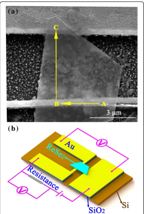
ReSe2flakes were synthesized by chemical-vapor-tran-sition on a copper substrate. A ReSe2 flake was trans-ferred to the Au electrodes to fabricate Au-ReSe2-Au contacts using the wetting transfer method, in which the ReSe2nanoribbon with the copper substrate was coated by polymethylmethacrylate (PMMA) and floated onto the etching solution to etch the copper substrate. After the copper substrate was peeled off, the PPMA-coated ReSe2flake was accurately moved above the Si substrate with Au nano-electrodes by the fixed-point transfer plat-form. Then, the PMMA was cut by laser and the PMMA-coated ReSe2 flake landed to be suspended be-tween the Au nanofilm and the Au nano-electrode. Fi-nally, the PMMA was removed by dipping the sample into a potassium hydroxide solution bath for 3 h. The scanning electron microscope (SEM) image of the fabri-cated Au electrode-ReSe2 flake-Au nanoribbon (Au-Re-Se2-Au) junctions in vertical view to the substrate is shown in Fig.1a. The ReSe2flake was in contact with an Au nanoribbon in section B and in contact with Au elec-trode in section C. Figure 1b shows the schematic dia-gram of the device.
The direction along A-B-C is defined as positive, or vice versa, and a direct current was applied. The voltage,
V, across the Au-ReSe2-Au junctions was measured by a high accuracy digital multimeter (Keitheley 2002, 8.5 digits), while the current, I, was determined through measuring the voltage across a reference resistor in series. TheI-Vcurves of the ReSe2/Au junctions for for-ward and inverse voltage were measured at different temperatures in a physical property measurement sys-tem (quantum design).
Results and Discussion
Figure2 shows the measuredI-Vcurves at 273 K, 280 K, 310 K, and 340 K. Significant asymmetries in the I-V
curves are observed at all the measured temperatures, indicating unusual rectifying behavior. Currents at 277
Fig. 1aSEM image of the device in vertical view to the substrate and the positive current direction andbschematic diagram of the measurement device
[image:2.595.305.539.86.434.2] [image:2.595.304.539.473.706.2]mV and−277 mV are used to calculate the current recti-fication ratio at each temperature, and the rectifying ra-tio is about 10. The current increases with the temperature for a given voltage.
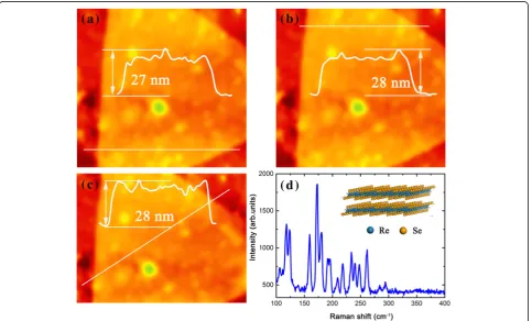
To explore the mechanism responsible for the unusual rectification, the microstructure of the ReSe2 flake was detected by an atomic force microscope [(AFM), Cypher, Oxford Instruments] and a Raman spectrometer (Jovin Yvon T64000, excitation wavelength 532 nm). The AFM image of the ReSe2flake is shown in Fig. 3a–c, and the determined average thickness is 28 nm based on the cross-sectional height profile along the white line. The Raman spectrum consisting of up to 13 expected lines with high signal strength is shown in Fig. 3d, corre-sponding well with the spectrum detected by Wolverson et al. [4] and revealing the triclinic crystal structure of the present ReSe2flake.
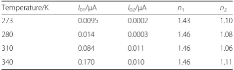
Figure4 is the SEM image of the ReSe2flake in slant view of 45° showing that the ReSe2 flake and the Au nanofilm are in contact with the Si substrate. ReSe2-Au contact has been shown the Ohmic contact in previous study [20] which is not responsible for the rectification behavior in this experiment. The circuit is constituted of the Au-ReSe2-Au and the Au-ReSe2-Si-Au junctions. Figure 5 shows the schematic of the circuit. The Si-Au contact has been shown the Schottky contact [21].
Figure 6 shows the energy dispersive spectroscopy (EDS) data. The map sum spectrum of ReSe2is acquired in section 1 and 2. The average chemical formula is ReSe1.67 which has a higher ratio of Re than ReSe2and gives the ReSe2 flake p-type semiconductor properties. Therefore, the ReSe2-Si contact is a p-n heterojunction and exhibits the rectification behavior. Asymmetry of both rectification contacts results in the rectification behavior.
Fig. 3a,b, andcAFM image and thickness of ReSe2, anddRaman spectrum and crystal structure of ReSe2
Fig. 4SEM image of the ReSe2flake and the Au nanofilm in slant
[image:3.595.306.539.87.241.2] [image:3.595.58.542.421.713.2]The current can be determined by the following equation in both the Schottky contact and the p-n heterojunction [22, 23]:
I¼I0eqV=nkT 1−e−qV=kT
ð1Þ
I0¼AAT2e−qΦB=kT ð2Þ
where I0 is the saturation current, q is the electronic charge, k is the Boltzmann constant, V is voltage ap-plied across the junction, A is the contact area, A* is the effective Richardson constant, ФB is the apparent barrier height, and T is the measurement temperature. The temperature-dependent ideality factorn represents the level that the contact departs from an ideal Schottky contact.
A calculation based on Eq. (1) is made to examine the analysis for the rectification behavior. Currents of the ReSe2-Si contact, I1, and the Si-Au contact, I2, are expressed by:
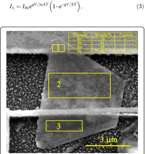
I1¼I01eqV=n1kT 1−e−qV=kT
; ð3Þ
I2¼I02e−qV=n2kT eqV=kT−1
: ð4Þ
Figure 7 shows that the numerical results agree well with experimental data. The numerical parameters are shown in Table 1. The reverse saturation current of the ReSe2-Si contact is larger than the Si-Au contact because the contact area of the ReSe2-Si contact is much larger as shown in Fig. 4. The reverse saturation current of both contacts increase with temperature, indicating that the electrical conductivities of both contacts exhibit rec-tification behavior as shown in Eq. (2).
The ideality factor of the ReSe2-Si contact is larger than the Si-Au contact due to different contact condi-tions and crystal structures. Figure4shows that the sur-face of the Si substrate is rough due to the etching solution, which makes the ReSe2-Si contact inhomogen-eous. The inhomogeneous contact leads to the large ideality factor [24,25]. The rough surface also produces a large number of trapping states which results in a large ideality factor [26]. Additionally, different contact types make different ideality factors. The ReSe2-Si contact is the p-n heterojunction, and the ReSe2and Si have differ-ent crystal structures, triclinic for ReSe2 and faced-centered cubic for Si. The lattice mismatch always leads to edge dislocation [27] and produces high density of trap states [26], making the ReSe2-Si contact deviate from the ideal contact and have a large ideality factor Fig. 5Schematic of the circuit
Fig. 6EDS data of ReSe2is on the top right corner of the image.
Boxes 1 and 2 represent two measured sections
[image:4.595.58.544.89.206.2] [image:4.595.56.292.453.704.2] [image:4.595.304.538.541.704.2][27]. The Si-Au is the metal semiconductor contact, and the crystal structure of Si has few effects on the ideality factor. The ideality factors of both contacts change little with temperature. It can be explained by Eq. (5) as re-ported by Khurelbaatar et al. [28],
n¼ q kT
dV
d lnI: ð5Þ
Equation (5) shows that the ideality factor is inversely proportional to the temperature. The ideality factor sig-nificantly decreases with temperature only at low temperature and changes slowly when the temperature is over 300 K [28,29]. However, as shown in Table1, the re-verse saturation current increases significantly with the temperature which is different from the ideality factor. It can be explained by Eq. (2). According to Eq. (2), the re-verse saturation current increases with temperature be-causeT2 and exp (−qΦB/kT) increase with temperature.
Due to the exponential relationship between exp (−qΦB/ kT) and−qΦB/kT, exp (−qΦB/kT) increases significantly
with temperature. Based on the research by Zhu et al [30],
qΦBof the Au/Si contact in the experiment at 273 K and
295 K are 0.77 eV and 0.79 eV, respectively. The calculated results show that the reverse saturation current at 295 K is six times as much as the reverse saturation current at 273 K, explaining why the reverse saturation current increases significantly with temperature.
Conclusions
In conclusion, a rectification behavior is observed in the contacts where a ReSe2 flake suspended across Au sub-strate and Au nanofilm at different temperature. The SEM image of the suspended ReSe2flake in slant view of 45° shows that the ReSe2flake and the Au nanofilm are in contact with the Si substrate and the EDS map illus-trated the elements composition, ReSe1.67. The contact between the ReSe2 flake and the Si substrate is respon-sible for the rectification behavior. The ReSe2-Si and Si-Au contacts are both rectification contacts forming another circuit, and asymmetry of both contacts results in the apparent rectification behavior. The calculated re-sults based on Schottky current equation considered the Si-Au Schottky contact, and the ReSe2-Si p-n hetero-junction agrees well with experiments results.
Abbreviations
2D:Two-dimensional; AFM: Atomic force microscope; EDS: Energy dispersive spectroscopy; FET: Field effect transistor; PMMA: Polymethylmethacrylate; SEM: Scanning electron microscope; TMD: Transition metal dichalcogenides
Acknowledgements
Not applicable
Funding
This work was supported by the National Natural Science Foundation of China (Grant Nos. 51776224, 51576105, 51636002, 51827807, and 51336009), the Science Fund for Creative Research Groups (Grant No. 51621062), Beijing Municipal Science & Technology Commission (No Z161100002116030), and the Tsinghua University Initiative Scientific Research Program.
Availability of Data and Materials
All data are fully available without restriction.
Authors’Contributions
All authors contributed to the preparation of the manuscript and to the discussion. All authors read and approved the final manuscript.
Competing Interests
The authors declare that they have no competing interests.
Publisher’s Note
Springer Nature remains neutral with regard to jurisdictional claims in published maps and institutional affiliations.
Author details
1
Beijing Key Laboratory of Process Fluid Filtration and Separation, College of Mechanical and Transportation Engineering, China University of
Petroleum-Beijing, Beijing 102249, China.2Key Laboratory for Thermal Science and Power Engineering of Ministry of Education, Department of Engineering Mechanics, Tsinghua University, Beijing 100084, China. 3Department of Chemistry, Tsinghua University, Beijing 100084, China.
Received: 24 October 2018 Accepted: 20 December 2018
References
1. Schmitsdorf RF, Kampen TU, Monch W (1997) Explanation of the linear correlation between barrier heights and ideality factors of real metal-semiconductor contacts by laterally nonuniform Schottky barriers. J Vac Sci Technol B 15(4):1221–1226.
2. Rhoderick EH (1982) Metal-semiconductor contacts. IEE Proc I Commun Speech Vis 129(1):1–14.
3. Cho AJ, Namgung SD, Kim H, Kwon JY (2017) Electric and photovoltaic characteristics of a multi-layer ReS2/ReSe2heterostructure. APL Materials 5:
076101.
4. Wolverson D, Crampin S, Kazemi AS, Ilie A, Bending SJ (2014) Raman spectra of monolayer, few-layer, and bulk ReSe2: an anisotropic layered
semiconductor. ACS Nano 8(11):11154–11164.
5. Zhang G, Zhang YW (2017) Thermoelectric properties of two-dimensional transition metal dichalcogenides. J Mater Chem C 5:7684–7698.
6. Pan T, Gong T, Yang W, Wu Y (2018) Numerical study on the thermal stress and its formation mechanism of a thermoelectric device. J Therm Sci 27(3): 249–258.
7. Zhou ZG, Zhu DS, Wu HX, Zhang HS (2013) Modeling, experimental study on the heat transfer characteristics of thermoelectric generator. J Therm Sci 22(1):48–54.
8. Morita SI, Tanimura K, Hayamizu Y, Yamada T, Horibe A, Haruki N (2016) Study of cycle output improvement by work-fluid including phase change material. J Therm Sci 25(6):558–563.
9. Qi X, Ma W, Zhang X, Zhang C (2018) Raman characterization and transport properties of morphology-dependent two-dimensional Bi2Te3nanofilms.
Appl Surf Sci 457:41–48.
10. Lopez-sanchez O, Lembke D, Kayci M, Radenovic A, Kis A (2013) Ultrasensitive photodetectors based on monolayer MoS2. Nat Nanotechnol
[image:5.595.55.292.109.180.2]8(7):497–501.
Table 1Calculated ideality factor for ReSe2-Si and Si-Au contacts
Temperature/K I01/μA I02/μA n1 n2
273 0.0095 0.0002 1.43 1.10
280 0.014 0.0003 1.46 1.08
310 0.084 0.011 1.46 1.06
11. Britnell L, Ribeiro RM, Eckmann A, Jalil R, Belle BD, Mishchenko A (2013) Strong light-matter interactions in heterostructures of atomically thin films. Science 340(6138):1311–1314.
12. Ross JS, Klement P, Jones AM, Ghimire NJ, Yan J, Mandrus DG (2014) Electrically tunable excitonic light-emitting diodes based on monolayer WSe2p–n junctions. Nat Nanotechnol 9(4):268–272.
13. Baugher BWH, Churchill HOH, Yang Y, Jarillo-Herrero P (2014) Optoelectronic devices based on electrically tunable p–n diodes in a monolayer dichalcogenide. Nat Nanotechnol 9:262–267.
14. Yang S, Wang C, Sahin H, Chen H, Li Y, Li SS, Suslu A, Peeters FM, Liu Q, Li J, Tongay S (2015) Tuning the optical, magnetic, and electrical properties of ReSe2by nanoscale strain engineering. Nano Lett 15(3):1660–1666.
15. Wang C, Yang S, Xiong W, Xia C, Cai H, Chen B, Wang X, Zhang X, Wei Z, Tongay S, Li J, Liu Q (2016) Gate-tunable diode-like current rectification and ambipolar transport in multilayer van der Waals ReSe2/WS2p-n
heterojunctions. Phys Chem Chem Phys 18(40):27750–27753.
16. Wang X, Huang L, Peng Y, Huo N, Wu K, Xia C, Wei Z, Tongay S, Li J (2016) Enhanced rectification, transport property and photocurrent generation of multilayer ReSe2/MoS2p-n heterojunctions. Nano Res 9(2):507–516.
17. Corbett CM, McClellan C, Rai A, Sonde SS, Tutuc E, Banerjee SK (2015) Field effect transistors with current saturation and voltage gain in ultrathin ReS2.
ACS Nano 9(1):363–370.
18. Corbet CM, Sonde SS, Tutuc E, Banerjee SK (2016) Improved contact resistance in ReSe2thin film field-effect transistors. Appl Phys Lett 108:
162104.
19. Park JY, Joe HE, Yoon HS, Yoo S, Kim T, Kang K, Min BK, Jun SC (2017) Contact effect of ReS2/metal interface. ACS Appl Mater Interfaces 9(31):
26325–26332.
20. Yang S, Tongay S, Li Y, Yue Q, Xia JB, Li SS, Li J, Wei SH (2014) Layer-dependent electrical and optoelectronic responses of ReSe2nanosheet
transistors. Nanoscale 6(13):7226–7231.
21. Balsano R, Matsubayashi A, LaBella VP (2013) Schottky barrier height measurements of Cu/Si(001), Ag/Si(001), and Au/Si(001) interfaces utilizing ballistic electron emission microscopy and ballistic hole emission microscopy. AIP Adv 3:112110.
22. Kang WP, Davidson JL, Gurbuz Y, Kerns DV (1995) Temperature-dependence and effect of series resistance on the electrical characteristics of a polycrystalline diamond metal-insulator-semiconductor diode. J Appl Phys 78(2):1101–1107.
23. Ito H (1986) Generation-recombination current in the emitter-base junction of AlGaAs/GaAs HBTs. Jpn J Appl Phys 25(9):1400–1404.
24. Tung RT (1991) Electron-transport of inhomogeneous Schottky barriers. Appl Phys Lett 58(24):2821–2823.
25. Sullivan JP, Tung RT, Pinto MR, Graham WR (1991) Electron-transport of inhomogeneous Schottky barriers - a numerical study. J Appl Phys 70(12): 7403–7424.
26. Gokarna A, Pavaskar NR, Sathaye SD, Ganesan V, Bhoraskar SV (2002) Electroluminescence from heterojunctions of nanocrystalline CdS and ZnS with porous silicon. J Appl Phys 92(4):2118–2124.
27. Majumdar S, Banerji P (2009) Temperature dependent electrical transport in p-ZnO/n-Si heterojunction formed by pulsed laser deposition. J Appl Phys 105:043704.
28. Khurelbaatar Z, Kil YH, Shim KH, Cho H, Kim MJ, Kim YT, Choi CJ (2015) Temperature dependent current transport mechanism in graphene/ germanium Schottky barrier diode. J Semicond Technol Sci 15(1):7–15. 29. Lee TC, Chen TP, Au HL, Fung S, Beling CD (1993) The effect of the
temperature-dependence of the ideality factor on metal-semiconductor solar devices. Semicond Sci Technol 8(7):1357–1360.