N A N O E X P R E S S
Open Access
CMOS-compatible metal-stabilized
nanostructured Si as anodes for lithium-ion
microbatteries
Gibaek Lee
1,2, Stefan L Schweizer
2and Ralf B Wehrspohn
1,2*Abstract
The properties of fully complementary metal-oxide semiconductor (CMOS)-compatible metal-coated nanostructured silicon anodes for Li-ion microbatteries have been studied. The one-dimensional nanowires on black silicon (nb-Si) were prepared by inductively coupled plasma (ICP) etching and the metal (Au and Cu) coatings by successive magnetron sputtering technique. The Cu-coated nb-Si show the most promising electrochemical performance enhancements for the initial specific capacity as well as their cyclability compared to pristine nb-Si. The electrochemical and microstructural properties before and after cycling of the metal-coated nb-Si compared to their pristine counterparts are discussed in detail.
Keywords:1-D nanowires on black silicon; Lithium-ion batteries; Electrochemical characterization; Anode materials; Metal coating
Background
Microbatteries are required to drive small devices, such as smartcards, medical implants, and sensors. To date, the electrochemical performances of these all-solid-state batteries are limited because planar thin films are employed as electrode and electrolyte materials. The thickness of the stacking films is typically limited below 15 μm, and thus, the resulting battery reveals relatively low power and energy densities. In order to develop im-proved electrochemical performances, new materials and complementary metal-oxide semiconductor (CMOS)-compatible high-throughput manufacturing processes are required. Large specific area substrates by nanoarchi-tectured electrodes may therefore represent a promising alternative to improve the general performances of these micro power sources [1-3]. Among various anode mate-rials in lithium-ion battery, Si has the highest theoretical specific capacity (approximately 4,200 mAh g−1, Li4.4Si), has a low Li uptake potential (approximately 0.4 V vs.
Li/Li+), and is completely CMOS compatible [4,5].
Unfortunately, Si-based electrodes suffer from poor capacity retention caused by a large volume change (ap-proximately 320%) of Si during Li insertion and extrac-tion. This feature leads to cracking and pulverization of Si-based electrodes induced by the large stresses, result-ing in a loss of electric contact and eventually capacity fading during cycling [6-8]. Various structural designs of Si-based electrodes have been suggested to overcome this disadvantage, such as nano- and microstructured Si, porous Si, and Si nanotubes [7,9-15]. These approaches have shown improved performance for Si materials in lithium-ion batteries. The nanostructured Si can provide sufficient intermediate space to withstand the large vol-ume expansion involved with Li insertion and thus allow for expeditious elastic strain associated with the degrad-ation upon cycling. Nevertheless, these Si nanostructures cannot be used commercially by now due to a difficult and expensive preparation process being mostly not compatible with standard silicon CMOS technology. Moreover, the formation of a solid/electrolyte interphase (SEI) at the interface layer between Si and the electrolyte is an obstacle for applications. Recently, it has been re-ported that metal silicide alloys composed of an active or inactive metal material can supply a capacity en-hancement and better cycle life of Si-based electrodes
* Correspondence:ralf.b.wehrspohn@iwmh.fraunhofer.de
1Fraunhofer Institute for Mechanics of Materials IWM, Halle (Saale) 06120,
Germany
2Department of Physics, Martin-Luther University of Halle-Wittenberg, Halle
(Saale) 06099, Germany
[16-19]. It has been suggested that this is probably due to the provision of a better contact and a better mechan-ical stability for nanostructured Si electrodes.
In contrast to [16-19], we examine in this paper the potential of a fully CMOS-compatible technology for metal-coated 1-D nanowires on black silicon (nb-Si) using inductively coupled plasma (ICP) etching and successive coating by metal magnetron sputtering. As we have shown recently, ICP-etched black silicon has the potential to be a cost-competitive candidate for large-area nanostructured silicon anodes [20]. Metallic
[image:2.595.60.539.85.553.2]additive materials for Si-based electrodes are classified as active materials and inactive materials. The active materials can be influenced by Li ions, whereas the in-active materials are impervious to Li ions. For compari-son and evaluation of both metallic additive materials, we used gold (Au) as a representative active metal material and copper (Cu) as an inactive metal material, respectively. We will show that also in the case of metal-coated nb-Si as anode, the electrochemical per-formance is better than in pristine nb-Si and discuss the influence of the metal thickness.
Figure 1Morphological characterization of the metal (Au, Cu)-coated nb-Si electrodes.Cross-sectional SEM images of the(a)Au-coated and(b)Cu-coated nb-Si electrodes showing where the elemental maps were obtained and corresponding element mapping images of Au, Cu, O, and Si for metal (Au, Cu)-coated nb-Si electrodes. The upper right images of (a) and (b) show the summarized elemental signals.
Leeet al. Nanoscale Research Letters2014,9:613 Page 2 of 8
Methods
Materials and preparation
The nb-Si anode has been provided by direct ICP
etch-ing with a gaseous mixture comprised of SiF6and C4F8
as discussed recently by us [20]. To achieve the deep nb-Si structure, the plasma etching process demands alternating plasma steps, including etching of Si and deposition of a passivation layer. This sequence etching process can gen-erate the highly ordered nanostructured black Si [20,21].
ICP etching was carried out on polished 525 ± 25 μ
m-thickn-type Si (100)-oriented wafers with a resistivity of 1 to 5 Ω cm. To remove the fluorinated groups (-CxFy-)
from the nb-Si surface induced by the ICP etching process, nb-Si was treated by heat. Afterwards, the wafer-scale nb-Si sample was broken into small pieces of suitable size of about 10 mm in diameter. Eventually, we prepared
long nb-Si electrodes with a length of 28 μm and a
diameter of approximately 730 nm. The average
dis-tance between the nanowires was about 1 μm. Au and
Cu were deposited onto the surface of the nb-Si elec-trode in a sputter coater (108auto, Cressington Scien-tific Instruments Ltd., Watford, Hertfordshire, UK), equipped with a high-resolution thickness monitor sys-tem (MTM10, Cressington Scientific Instruments Ltd., Watford, Hertfordshire, UK). We prepared four metal (Au, Cu)-coated nb-Si electrodes with a thickness of 20 and 50 nm, respectively.
Measurements
Electrochemical measurements of the nb-Si electrode were carried out by using Swagelok cells (Swagelok Company, Solon, OH, USA). Li metal foil was used as a counter/reference electrode. The backside of the nb-Si
was contacted mechanically with Cu foil as a current collector without binder and electronic conductive ma-terial. Both cathode and anode electrodes were separated by a glass fiber filter paper (Whatman GF/B, Sigma-Aldrich, St. Louis, MO, USA), wetted with electrolyte. The electrolyte was 1 M LiPF6in 1:1 (w/w) ethylene car-bonate (EC) and diethyl carcar-bonate (DEC) (Merck KGaA, Darmstadt, Germany). The cycling of the nb-Si electrode has been performed using the galvanostatic charge/dis-charge electrochemical technique with the Neware battery testing system (Neware Technology Limited., Shenzen, China). These cells were assembled and disassembled in an Ar-filled glove box (<0.1 ppm oxygen) at room temperature. The specific capacity of nb-Si was calcu-lated based on the bare surface area. The discharge sequence represents lithiation due to the Si anode cell in this work. The surface morphology was characterized by field-emission scanning electron microscopy (FE-SEM, JSM-7401 F, JEOL Ltd., Tokyo, Japan) and energy-dispersive spectroscopy, and the X-ray diffraction (XRD) patterns were obtained by D/MAX-2200 V/PC (Rigaku, Tokyo, Japan) with Cu Kαradiation.
Results and discussion
[image:3.595.59.540.89.311.2]Figure 1 shows SEM images of the as-prepared Au- and Cu-coated nb-Si electrodes, respectively. The vertically aligned Si structures were obtained by direct sequence ICP etching and magnetron sputtering technique on the Si substrate. As an original part of the Si substrate, the nb-Si ensures an effective charge transport through dir-ect eldir-ectric pathways. The element distribution of the metal coating was characterized by energy-dispersive X-ray spectroscopy (EDS) mapping. The Au and Cu images
show the uniform lateral distribution of the metal along the nanowires with hardly any agglomeration. However, an intense signal of the metal was detected in the upper part, resulting from the fact that the metal elements can only penetrate into the top part of the nb-Si due to the physical nature of the sputtering process. The oxygen images are attributed to the surface oxidation covering nb-Si, and the Si images correspond to the morphology of nb-Si electrodes in the SEM images, respectively. These results confirm that the metal-coated nb-Si elec-trode is composed of silicon nanowires covered with a uniform Au and Cu coating with a small amount of na-tive oxide on the nb-Si surface.
To determine the structural properties of metal-coated nb-Si, XRD patterns of the metal-coated nb-Si were
compared with those of the pristine nb-Si. Figure 2 shows XRD patterns of Cu-coated, Au-coated, and pris-tine nb-Si. The XRD patterns of metal-coated nb-Si indi-cate that diffraction peaks are associated with crystalline structures of Au (111), (200), (220), and (311) regarding Au-coated Si, and Cu (111) regarding Cu-coated nb-Si, respectively. In addition, peaks of crystalline silicon were detected, such as (111), (220), and (311). The in-tensity of the Si (400) peak at ca. 70 2θis high compared to others induced by the large crystalline Si substrate.
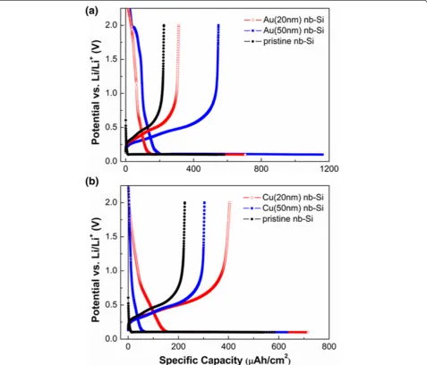
[image:4.595.60.538.295.703.2]To investigate the cycling performance of metal (Au, Cu)-coated nb-Si electrodes, we used the galvanostatic electrochemical technique at a constant current density of 50μA cm−2. The voltage range was from 0.1 to 2.0 V (vs. Li/Li+). Figure 3a shows the first charge/discharge
Figure 3Initial galvanostatic charge/discharge curves of the nb-Si electrode.The voltage range is between 0.1 and 2.0 V (vs. Li/Li+) at a constant
current density of 50μA cm−2. The first cycle of the(a)Au-coated and(b)Cu-coated nb-Si electrode compared with that of the pristine nb-Si electrode.
Leeet al. Nanoscale Research Letters2014,9:613 Page 4 of 8
curves of 20- and 50-nm Au-coated nb-Si. The first
dis-charge capacity reached 705.5 and 1,161.5 μAh cm−2
with a coulombic efficiency of 44.3% and 47.2%, respect-ively. This is significantly higher than that of pristine nb-Si. Moreover, the discharge capacity of Au(50)-coated nb-Si is higher than that of Au(20)-coated nb-Si. This is because Au could contribute to form Au-Li-Si alloys as an active material for lithium-ion battery systems. In com-parison, the first discharge capacity of Cu(20)- and Cu (50)-coated nb-Si was 716.1 and 632.7μAh cm−2, giving a coulombic efficiency of 56.6% and 47.9%, respectively, in Figure 3b. This is still slightly higher compared to pristine nb-Si as well. However, the increase is not as strong as in the case of the Au coating since Cu is an inactive material. In addition, the discharge capacity of the thin Cu(20) coat-ing is slightly higher than that of the thick Cu(50) coatcoat-ing in contrast to the Au coatings. Regarding the influence of the different thicknesses of Au and Cu, the Au coating shows a significant enhancement in capacity with increas-ing thickness of Au. In contrast, the thickness of the Cu coating has hardly any influence on the specific capacity at the first cycle. Note that all prepared metal-coated nb-Si electrodes show a relative low coulombic efficiency of around 50%, mainly resulting from the slow reaction paths along the huge specific surface area. Figure 4 shows the discharge capacity of the metal-coated nb-Si electrode versus cycle number at a constant current density of
50 μA cm−2. Whereas pristine nb-Si has a remaining
capacity of only 24% after 20 cycles, the 50-nm Cu-coated samples still have about 70% (Table 1).
[image:5.595.61.539.89.307.2]Our electrochemical cycling results show that the metal coating can improve not only the discharge cap-acity but also the capcap-acity retention compared to pris-tine nb-Si, confirming previous results on other silicon nanostructures [9,16-18] and extending it to CMOS-compatible processes. Therefore, we further investigated with cyclic voltammetry (CV) the Au-coated and Cu-coated nb-Si electrodes in the potential range between 0.01 and 2.5 V (vs. Li/Li+) at a scan rate of 0.5 mV s−1 (as shown in Figure 5). In Figure 5a for the Au-coated nb-Si, a characteristic peak at about 0.15 V indicates the onset of formation of the Li-Si alloy during discharging, and a peak at about 0.5 V implies the Li-Si de-alloying during charging. These peaks have shifted to a slightly higher potential of approximately 0.25 V and appro-ximately 0.6 V, respectively, during cycling. In the same
[image:5.595.305.537.625.717.2]Figure 4Discharge capacities versus cycle number for the nb-Si electrodes.Plot of the discharge capacities for the Au-coated (red squares) and Cu-coated (blue triangles) nb-Si electrodes compared with the pristine (black circles) nb-Si electrode. The performance cycle condition is the same as for Figure 3.
Table 1 Discharge capacity and capacity retention of pristine nb-Si and metal (Au, Cu)-coated nb-Si electrodes
Sample 1st
(μAh cm−2) 20th(
μAh cm−2) Capacityretention (%)
Pristine nb-Si 582.3 142.3 24.4
Au(20)-coated nb-Si 705.3 389.0 55.2
Au(50)-coated nb-Si 1,161.5 352.1 30.3
Cu(20)-coated nb-Si 716.1 363.3 50.7
Cu(50)-coated nb-Si 632.7 440.4 69.6
Constant current density of 50μA cm−2
manner, the Cu-coated nb-Si electrode shows a simi-lar phenomenon at the first cycle as shown in Figure 5b. However, the following cycles show a dif-ferent behavior. In the case of the Au-coated nb-Si electrode, the current peak increased rapidly within about 15 cycles since Au as an active material leads to an increasing specific capacity by forming Au-Li-Si al-loys, as mentioned before, and then stagnated or de-creased a little after subsequent cycles. In contrast, the current peak of the Cu-coated nb-Si electrode in-creased gradually up to the 30th cycle. Note that the Au metal is more active with Li-Si alloying/de-alloying than the Cu metal at the beginning of cycles, resulting in the initial high specific capacity. To further verify
the improved behavior of the morphology and volume changes of metal-coated nb-Si, particularly the Cu-coated samples, we performed SEM analysis of the metal-coated nb-Si at a full delithiation after 50 cycles compared to a pristine one (as shown in Figure 6). Most of the metal-coated nb-Si retained their original shape without cracking or fracturing. The metal-coated nb-Si show only slight deformations and volume changes, resulting from the amorphization during continuous cycling.
Conclusions
[image:6.595.58.543.88.511.2]We developed a fully CMOS-compatible technology for the fabrication of Au- and Cu-coated nb-Si anodes for
Figure 5Cyclic voltammograms for the metal (Au, Cu)-coated nb-Si electrodes.The cycle voltage range is between 0.01 and 2.5 V (vs. Li/Li+) at scan rate of 0.5 mV s−1. Plot of cyclic voltammograms for the(a)Au-coated and(b)Cu-coated nb-Si electrodes.
Leeet al. Nanoscale Research Letters2014,9:613 Page 6 of 8
microbatteries with a similar capacity and stability com-pared to conventional carbon-based technologies. The silicon nanowire anodes are prepared by ICP etching method of silicon and successive magnetron sputtering of metals. In particular, Cu-coated (50 nm) nb-Si has the lowest capacity fading and a stable capacity reten-tion during cycling. The difference of the electrochem-ical properties of Cu and Au can be explained by the better adhesion of copper on silicon in line with recent in situ experiments [22]. We believe further improve-ments of the capacity can be made by continuing to optimize the electrolyte/anode interface.
Abbreviations
CMOS:complementary metal-oxide semiconductor; ICP: inductively coupled plasma; SEI: solid/electrolyte interphase.
Competing interests
The authors declare that they have no competing interests.
Authors’contributions
GL designed the experiments, performed the fabrication and the
[image:7.595.59.539.89.531.2]measurements, and managed the interpretation of data. GL and SLS drafted the manuscript. RBW supervised the project. All authors discussed the results and commented on the manuscript. All authors read and approved the final manuscript.
Figure 6Cross-sectional SEM images of the nb-Si electrode after 50 cycles.The cells were charged to 2.0 V (vs. Li/Li+).(a)Pristine nb-Si and
Acknowledgements
This study was performed with assistance from the research fund of the Fraunhofer Institute for Mechanics of Materials IWM.
Received: 26 September 2014 Accepted: 5 November 2014 Published: 14 November 2014
References
1. Roberts M, Johns P, Owen J, Brandell D, Edstrom K, El Enany G, Guery C, Golodnitsky D, Lacey M, Lecoeur C, Mazor H, Peled E, Perre E, Shaijumon MM, Simon P, Taberna PL:3D lithium ion batteries—from fundamentals to fabrication.J Mater Chem2011,21:9876–9890.
2. Scrosati B, Garche J:Lithium batteries: status, prospects and future.
J Power Sources2010,195:2419–2430.
3. Ellis BL, Knauth P, Djenizian T:Three-dimensional self-supported metal oxides for advanced energy storage.Adv Mater2014,26:3368–3397. 4. Huggins RA:Lithium alloy negative electrodes.J Power Sources1999,
81:13–19.
5. Szczech JR, Jin S:Nanostructured silicon for high capacity lithium battery anodes.Energy Environ Sci2011,4:56–72.
6. Beaulieu L, Hatchard T, Bonakdarpour A, Fleischauer M, Dahn J:Reaction of Li with alloy thin films studied by in situ AFM.J Electrochem Soc2003,
150:A1457–A1464.
7. Chan CK, Peng H, Liu G, McIlwrath K, Zhang XF, Huggins RA, Cui Y:
High-performance lithium battery anodes using silicon nanowires.
Nat Nanotechnol2007,3:31–35.
8. Li H, Huang X, Chen L, Wu Z, Liang Y:A high capacity nano Si composite anode material for lithium rechargeable batteries.Electrochem Solid State Lett1999,2:547–549.
9. Shin H, Corno JA, Gole JL, Liu M:Porous silicon negative electrodes for rechargeable lithium batteries.J Power Sources2005,139:314–320. 10. Kang D, Corno JA, Gole JL, Shin H:Microstructured nanopore-walled
porous silicon as an anode material for rechargeable lithium batteries.
J Electrochem Soc2008,155:A276–A281.
11. Cui L, Ruffo R, Chan CK, Peng H, Cui Y:Crystalline-amorphous core-shell silicon nanowires for high capacity and high current battery electrodes.
Nano Lett2008,9:491–495.
12. Kim H, Han B, Choo J, Cho J:Three‐dimensional porous silicon particles for use in high‐performance lithium secondary batteries.Angew Chem Int Edit2008,120:10305–10308.
13. Song T, Xia J, Lee J, Lee DH, Kwon M, Choi J, Wu J, Doo SK, Chang H, Park WI, Zang DS, Kim H, Huang Y, Hwang K, Rogers A, Paik U:Arrays of sealed silicon nanotubes as anodes for lithium ion batteries.Nano Lett2010,
10:1710–1716.
14. Park M, Kim MG, Joo J, Kim K, Kim J, Ahn S, Cui Y, Cho J:Silicon nanotube battery anodes.Nano Lett2009,9:3844–3847.
15. Astrova E, Fedulova G, Smirnova I, Remenyuk A, Kulova T, Skundin A:
Porous silicon based negative electrodes for lithium ion batteries.
Tech Phys Lett2011,37:731–734.
16. Sethuraman VA, Kowolik K, Srinivasan V:Increased cycling efficiency and rate capability of copper-coated silicon anodes in lithium-ion batteries.
J Power Sources2011,196:393–398.
17. Ossei‐Wusu E, Cojocaru A, Hartz H, Carstensen J, Föll H:Silicon nanowires made via macropore etching for superior Li ion batteries.Phys Status Solidi A2011,208:1417–1421.
18. Vlad A, Reddy AL, Ajayan A, Singh N, Gohy JF, Melinte S, Ajayan PM:Roll up nanowire battery from silicon chips.Proc Natl Acad Sci U S A2012,
109:15168–15173.
19. Thakur M, Isaacson M, Sinsabaugh SL, Wong MS, Biswal SL:Gold-coated porous silicon films as anodes for lithium ion batteries.J Power Sources
2012,205:426–432.
20. Lee G, Schweizer SL, Wehrspohn RB:Electrochemical characteristics of plasma-etched black silicon as anode for Li-ion batteries.J Vac Sci Technol A2014,32:061202.
21. Volland B, Shi F, Hudek P, Heerlein H, Rangelow IW:Dry etching with gas chopping without rippled sidewalls.J Vac Sci Technol B1999,
17:2768–2771.
22. McDowell MT, Woo Lee S, Wang C, Cui Y:The effect of metallic coatings and crystallinity on the volume expansion of silicon during
electrochemical lithiation/delithiation.Nano Energy2012,1:401–410.
doi:10.1186/1556-276X-9-613
Cite this article as:Leeet al.:CMOS-compatible metal-stabilized nanostructured Si as anodes for lithium-ion microbatteries.Nanoscale Research Letters20149:613.
Submit your manuscript to a
journal and benefi t from:
7Convenient online submission 7Rigorous peer review
7Immediate publication on acceptance 7Open access: articles freely available online 7High visibility within the fi eld
7Retaining the copyright to your article
Submit your next manuscript at 7 springeropen.com
Leeet al. Nanoscale Research Letters2014,9:613 Page 8 of 8