N A N O E X P R E S S
Open Access
Impact of program/erase operation on the
performances of oxide-based resistive switching
memory
Guoming Wang
1,2, Shibing Long
1*, Zhaoan Yu
1, Meiyun Zhang
1, Yang Li
1, Dinglin Xu
1, Hangbing Lv
1, Qi Liu
1,
Xiaobing Yan
1, Ming Wang
1, Xiaoxin Xu
1, Hongtao Liu
1, Baohe Yang
2and Ming Liu
1Abstract
Further performance improvement is necessary for resistive random access memory (RRAM) to realize its
commercialization. In this work, a novel pulse operation method is proposed to improve the performance of RRAM based on Ti/HfO2/Pt structure. In the DC voltage sweep of the RRAM device, the SET transition is abrupt under positive bias. If current sweep with positive bias is utilized in SET process, the SET switching will become gradual, so SET is current controlled. In the negative voltage sweep for RESET process, the change of current with applied voltage is gradual, so RESET is voltage controlled. Current sweep SET and voltage sweep RESET shows better controllability on the parameter variation. Considering the SET/RESET characteristics in DC sweep, in the
corresponding pulse operation, the width and height of the pulse series can be adjusted to control the SET and RESET process, respectively. Our new method is different from the traditional pulse operation in which both the width and height of program/erase pulse are simply kept constant which would lead to unnecessary damage to the device. In our new method, in each program or erase operation, a series of pulses with the width/height gradually increased are made use of to fully finish the SET/RESET switching but no excessive stress is generated at the same time, so width/height-controlled accurate SET/RESET can be achieved. Through the operation, the uniformity and endurance of the RRAM device has been significantly improved.
Keywords:Resistive random access memory (RRAM); Current sweep; Pulse operation; Uniformity; Endurance; Weibull distribution
Background
Thanks to the increasing demand from portable electronic products like smartphones, cameras, and laptops, the de-mand for solid-state memories has been increasing rapidly in recent years. However, in the further scaling down, the traditional flash memory is facing more and more prob-lems due to its physical limitations. Although innovations in cell structure and device materials may help extend flash memory for another couple of technology nodes, alternative candidates must be explored for future non-volatile memory (NVM) applications. Among various candi-dates, resistive random access memory (RRAM) is the most promising one for future high-density NVM application,
owning to its characteristics of simple cell structure, fast program/erase (P/E) speed, excellent scalability, low oper-ation power consumption, and good compatibility with the standard complementary metal-oxide-semiconductor (CMOS) process [1-5]. However, in order to meet the practical application requirements, the performances of RRAM demonstrated to date still need improvements in the following areas: (1) effective control of high and low resistance state; (2) minimization of the variations of re-sistive switching parameters. Some approaches have been proposed to improve the operation test method of RRAM. Nevertheless, few works systematically studied the detailed influence of DC and pulse program/erase operations on the performances of oxide-based RRAM. In this work, aiming at addressing the above challenges, we try to eluci-date the impact of P/E operation on the performances through comprehensive device characterizations and to * Correspondence:[email protected]
1
Lab of Nanofabrication and Novel Device Integration, Institute of Microelectronics, Chinese Academy of Sciences, Beijing 100029, China Full list of author information is available at the end of the article
explore possible solutions through innovations in test and operation methods.
For the necessity of plenty of DC and pulse measure-ment, stable valence change mechanism (VCM) devices with Ti/HfO2/Pt structure [5-12] is made use of in this work. In the DC positive voltage sweep the SET transition is abrupt, but it becomes gradual under current sweep. The RESET process is gradual in negative voltage sweep. So SET and RESET are current and voltage controlled, re-spectively. Combining positive current sweep SET and corresponding negative voltage sweep RESET operation, stable and uniform distributions of on-state and off-state resistance can be obtained. Gaining inspiration from the DC SET/RESET characteristics, we proposed a novel pulse operation scheme, i.e. the width and height of the pulse series are adjusted to control the SET and RESET process, respectively. Our new method is different from the trad-itional pulse operation with single constant program/ erase pulse. Thus, accurate SET/RESET controlled by pulse width/height can be achieved through our new method. As a result of the new method, the uniformity and endurance of the RRAM device has been signifi-cantly improved.
Methods
Resistive switching memory devices with Ti/HfO2/Pt struc-ture were fabricated as follows. First, after the standard chemical cleaning of the silicon substrate, a SiO2film with a thickness of 100 nm was thermally grown through dry oxidation method. Then, Ti/Pt bilayer with thickness of 30/70 nm was sequentially deposited by e-beam evapor-ation to act as the bottom electrode (BE). Next, a high-quality 8-nm-thickness HfO2resistive switching layer was grown by atom layer deposition (ALD) technology, which has the advantage of well controlling on the deposition pa-rameters and excellent deposition uniformity. Finally, the 10/70-nm-thickness Ti/Pt bilayer or 70-nm-thickness Cu film was prepared by e-beam evaporation and then pat-terned by lift-off process to form the top electrode (TE).
The area of TE is defined as 100 × 100 μm2. The DC
electrical characteristics of the devices were measured by Keithley 4200-SCS semiconductor characterization system, where the Pt BE was grounded while the bias voltage was applied on the Ti/Pt or Cu TE. In the traditional pulse measurement, a single pulse was usually employed to fulfill the SET/RESET operation, and a small read pulse or a vis-ual tool was used to verify if the SET/RESET is completed and to measure the switching time. In the height/width-adjusting pulse operation measurement, Keithley 4205-PG2 pulse generator was used to generate program/erase pulse series by an automatic procedure, and the device states were read by Keithley 4200-SCS. A matrix Keithley 707A is used to carry out the switching between the pulse pro-gram/erase operation and DC read operation.
Results and discussion
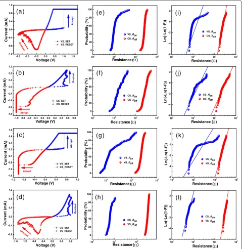
Figure 1a-d shows theI-Vcurves under four types of DC
sweep measurement of the Ti/HfO2/Pt VCM device. The device works in bipolar switching mode, i.e. SET occurs in positive polarity while RESET is in negative bias. In the DC voltage sweep (VS) of the RRAM device (Figure 1a), the SET transition is abrupt under positive bias, while the change of current with applied voltage in RESET process is gradual in the negative voltage sweep, so the RESET operation is a voltage-controlled procedure. In the DC current sweep (CS) as shown in Figure 1b, it is in the op-posite that the SET switching is a gradual so it is a current-controlled procedure. Since the abrupt SET process happens acrimoniously, it will produce large over-shoot current, leading to great damage to RRAM device. Nevertheless, the gradual process will reduce the over-shoot current and the controllability on the resistance value is easy to be achieved. Consequently, by combining the positive current sweep SET and the corresponding negative voltage sweep RESET operation, i.e. by integrat-ing current-controlled SET and voltage-controlled RESET, as shown in Figure 1d, we can obtain an effective way to make the SET and RESET process to gently and gradually evolve. From Figure 1c, both abrupt SET and RESET pro-cesses are obtained by positive voltage sweep SET and cor-responding negative current sweep RESET operation.
The statistical distributions of on-state and off-state resist-ance with different DC SET/RESET operation were studied. Figure 1e-h shows the cumulative distributions of Ronand
Roff in 200 continuous cycles measured with the operation modes in Figure 1a-d, respectively. Comparing the results shown in Figure 1e-h, the distribution of Ron acquired by current-controlled SET is more uniform than that got by voltage sweep SET. At the same time, the uniformity ofRon
and Roff measured by CS-SET and VS-RESET is also
im-proved compared with that by CS-SET and CS-RESET. These results can also be seen from Table 1. The coefficient of variation (σ/μ) ofRondecreases from 52.2% in Figure 1f to 23.4% in Figure 1h. Moreover, σ/μ ofRoff has also im-proved from 30.6% to 11.1%. The Weibull distribution is widely used in reliability forecast and evaluation [13-18]. The Weibull distribution is described by F= 1−exp[−(x/
slopes ofRonandRoffdistributions. In consequence, stable and uniform distributions of low and high resistance states can be obtained by the gradual SET and RESET operations.
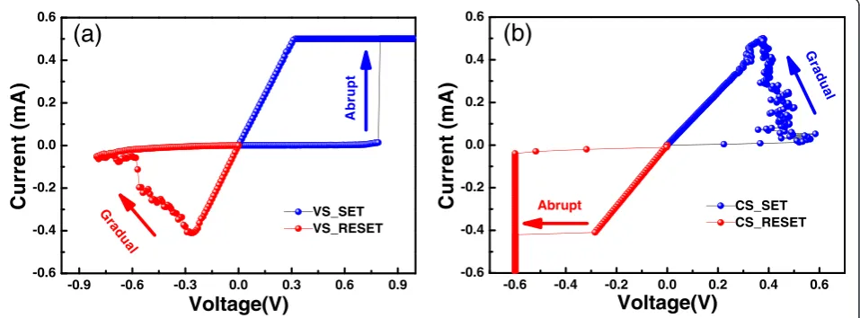
We have also found that the current-controlled SET op-eration and voltage-controlled RESET opop-eration are suit-able for other kinds of RRAM devices. Figure 2a,b shows
the typical I-V curves of electrochemical mechanism
(ECM) device with Cu/HfO2/Pt structure measured by DC voltage sweep and DC current sweep, respectively. Similar effect in controlling the SET/RESET process can be achieved, i.e. gradual SET can be got by current sweep and RESET is progressive under voltage sweep.
Considering the above SET/RESET characteristics in DC sweep, we use a new pulse operation to achieve the
-1.5 -1.0 -0.5 0.0 0.5 1.0 1.5 -1.2 -0.8 -0.4 0.0 0.4 0.8 1.2 Cur re nt (m A) Voltage (V) VS_SET VS_RESET A b rupt Gr ad ua l 102 103 104 105 0 20 40 60 80 100 VS_Ron CS_Roff P ro b a b ilit y (% )
Resistance ( ) 10 2 103 104 105 -6 -4 -2 0 2 VS_Ron CS_Roff
Resistance ( )
Ln(
-Ln(
1
-F)
)
-1.2 -0.8 -0.4 0.0 0.4 0.8 1.2 -1.6 -1.2 -0.8 -0.4 0.0 0.4 0.8 1.2 Abrupt A b rupt Cur re n t (mA) Voltage (V) VS_SET CS_RESET 102 103 104 105 0 20 40 60 80 100 CS_Ron CS_Roff P ro b a b ilit y (% ) Resistance ( 102 103 104 105 -6 -4 -2 0 2 CS_Ron VS_Roff Ln( -Ln( 1 -F) )
Resistance ( ) 103 104 105 0 20 40 60 80 100
Resistance ( )
Pro b ab il ity (% ) VS_Ron VS_Roff 102 103 104 105 -6 -4 -2 0 2 VS_Ron VS_Roff
Resistance ( )
Ln( -Ln( 1 -F )) 102 103 104 105 -6 -4 -2 0 2 CS_Ron CS_Roff
Resistance ( ) ) L n (-L n (1-F )) 102 103 104 0 20 40 60 80 100 CS_Ron VS_Roff P ro b a b ilit y (% )
Resistance ( )
(i)
(l)
(k )
(g )
-1.0 -0.8 -0.6 -0.4 -0.2 0.0 0.2 0.4 0.6 0.8 -1.6 -1.2 -0.8 -0.4 0.0 0.4 0.8 1.2 Abrupt G radual C u rren t (m A ) Voltage (V) CS_SET CS_RESET
-1.6 -1.2 -0.8 -0.4 0.0 0.4 0.8 -0.8 -0.4 0.0 0.4 0.8 1.2 Gr ad ual Cur re nt (m A) Voltage (V) CS_SET VS_RESET Gr a d u a l
(a )
(h )
(f)
(e )
(d )
(c )
[image:3.595.59.539.89.582.2](b )
(j)
Figure 1TypicalI-Vcurves and statistical distributions of Ti/HfO2/Pt RRAM device under different operation. (a)Positive voltage sweep SET
and negative voltage sweep RESET processes.(b)Positive current sweep SET and negative current sweep RESET processes.(c)Positive voltage sweep SET and negative current sweep RESET processes.(d)Positive current sweep SET and negative voltage sweep RESET processes.(e-h)The cumulative distributions ofRonandRoffin 200 continuous cycles tested by the operation modes in(a-d), respectively.(i-l)The Weibull plots of the distributions of
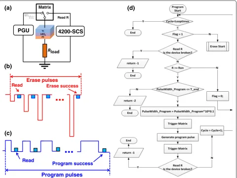
same effects. Figure 3a shows the test circuit of our new method. Pulses generated by PGU with width/height in-creased by an automatic procedure are applied on the RRAM device to finish the P/E operation. After each pulse, the connection is switched to 4200-SCS to carry out the DC read operation. Figure 3b,c shows in a more accurate way the schematic diagram of one complete erase process with height-adjusting pulse operation and one complete program process with width-adjusting pulse operation, respectively. Figure 3d provides the detailed flow chart of program test for our new pulse operation method. The width of the program pulses increases by around 1.1 times for each program-verify cycle. When the width exceeds the maximum pulse
width tend, the procedure will be terminated. The flow
chart of erase operation is similar to that of program test, and the height of erase pulse also increases about 1.1 times for each erase-verify cycle.
Figure 4 reveals the gradual change of the resistance using the width-adjusting program pulse operation and the height-adjusting erase pulse operation. The resistance gradually increases with time by the novel width-adjusting
program pulse operation and gradually decreases with voltage through the height-adjusting erase pulse operation. Similar to the resistance adjusting by DC sweep method [22-25], our pulse operation methods can not only realize the gradual change of the resistances but can also be uti-lized to acquire multi-level storage of RRAM [26-29].
During our new pulse operation, on-state and off-state resistance were respectively setup to the average value of
Ron and Roff measured in DC sweep. After each pulse
program or erase operation, the test circuit is switched by the matrix to 4200 to read the resistance (Figure 3a, d). When the resistance of the device is less than 30Ω, we assume that the device is damaged, and the test will be stopped automatically. Figure 5 shows the compari-son of the cumulative distributions ofRonand Roff mea-sured by traditional single pulse operation and our new pulse operation. It can be seen that the coefficient of
variation ofRonhas changed from 31.48% to 26.78% and
that of Roff has been greatly improved from 40.87% to
[image:4.595.59.538.103.198.2]12.24%. Therefore, stable and uniform distributions of on-state and off-on-state resistance can be obtained by accurately controlling the SET/RESET switching by adjusting the Table 1 The distributions ofRonandRoffunder different operation modes
Operation VS_SET and VS_RESET CS_SET and CS_RESET VS_SET and CS_RESET CS_SET and VS_RESET SP_P and SP_E AP_P and AP_E
Parameters Ron Roff Ron Roff Ron Roff Ron Roff Ron Roff Ron Roff
σ(kΩ) 0.716 3.7178 1.006 8.930 3.933 4.368 0.157 3.549 0.181 4.376 0.117 1.552
μ(kΩ) 1.218 25.338 1.927 29.154 3.513 24.494 0.673 32.051 0.575 10.708 0.453 12.687
σ/μ 0.588 0.147 0.522 0.306 1.119 0.178 0.234 0.111 0.315 0.409 0.268 0.122
β 5 9 3 3.4 2.1 6.7 6.5 10.5 3.5 5 5 10
R63%(kΩ) 1.274 26.425 1.945 32.233 2.582 26.049 0.700 33.010 0.637 10.427 0.491 13.976
The comparison of four DC operation methods and two pulse operation methods on their controllability to the variation in Ti/HfO2/Pt RRAM device are listed in
the above.
σis the standard deviation,μis the mean value,σ/μis the coefficient of variation, andβandR63%are the shape factor (or Weibull slop) and scale factor of the
Weibull distributions of resistances, respectively.
-0.9 -0.6 -0.3 0.0 0.3 0.6 0.9 -0.6
-0.4 -0.2 0.0 0.2 0.4 0.6
Gr ad
u al
VS_SET VS_RESET
Ab
ru
p
t
Cu
rr
e
n
t
(mA)
Voltage(V)
(a)
-0.6 -0.4 -0.2 0.0 0.2 0.4 0.6 -0.6
-0.4 -0.2 0.0 0.2 0.4 0.6
Abrupt
Gr a d
u al
CS_SET CS_RESET
Cu
rr
e
n
t
(m
A)
Voltage(V)
[image:4.595.60.539.529.706.2](b)
Figure 2The typicalI-Vcurves of Cu/HfO2/Pt RRAM device under two modes. (a)Voltage sweep SET and RESET.(b)Current sweep SET
Figure 3The testing schematic of pulse operation method. (a)The test circuit of our new pulse operation method. Pulses with width or height increased by the automatic procedure are applied to finish the program or erase operation, respectively.(b)Schematic diagram of one complete erase process with height-adjusting pulse operation.(c)Schematic diagram of one complete program cycle of width-adjusting pulse operation.(d)A detailed flow chart of the program method.
0 30 60 90 120 150 180 210 240
4x10³ 8x10³ 1x10⁴ 2x10⁴ 2x10⁴
Time
(ns
)Adjust Width
R
esi
st
ance
()
0 -1 -2 -3 -4 -5
2x10³ 4x10³ 6x10³ 8x10³ 1x10⁴
Adjust Height
Voltage (V)
R
esi
st
ance
()
(b)
(a)
[image:5.595.59.539.509.703.2]pulse width/height, which is similar to the DC sweep mode.
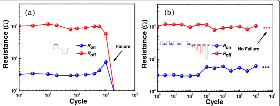
Figure 6 shows the endurance characteristics measured by traditional single pulse operation and our new pulse operation. As can be seen from Figure 6a, the endurance tested with traditional pulse method is usually less than 103 switching cycles, where the pulse amplitude/width is
setup as 1 V/1μs for program operation and 3 V/100 ns
for erase operation. However, from Figure 6b, it is surprising that more than 106switching cycles have been obtained by our new pulse operation and the device still works well without failure. Here, the height and width of the program pulses are setup as 1 V and from 20 ns (ini-tial) to 1 s (tend), respectively. The width and amplitude of
the erase pulse are setup as 100 ns and from −0.5 V
(initial) to−10 V (Vend). The remarkable improvement in endurance is attributed to the appropriate program/erase operation in each cycle, without any inadequate operation and over-operation.
Conclusions
We have investigated the impact of DC and pulse program/ erase operation on the uniformity and endurance perfor-mances of Ti/HfO2/Pt-based RRAM device. Appropriate program/erase conditions are necessary to acquire the uni-form resistive switching. A width-adjusting program and the height-adjusting erase pulse operation method are pro-posed. Our new method is advantageous to obtain the
[image:6.595.61.538.88.283.2](a)
(b)
Figure 5The statistical distributions ofRon andRoff. (a)The cumulative distributions ofRonandRoffobtained through width/height-adjusting
pulses (AP) and single pulse (SP) operation.(b)The Weibull distributions ofRonandRoff.RonandRoffmeasured by our new pulse method have good
uniformity.
100 101 102 103 104 105 106 107 102
103 104
...
...
No Failure Ron
Roff
R
e
si
st
ance
(
)
Cycle
(a )
(b )
100 101 102 103 104
102 103 104
Failure
R
esi
st
ance
(
)
Ron Roff
[image:6.595.61.539.524.705.2]Cycle
Figure 6Endurance characteristics of Ti/HfO2/Pt RRAM device.The comparison of endurance measured by traditional single pulse operation
moderate program/erase operation in each cycle, without any inadequate operation and over operation. Thus, the en-durance performance of the device is greatly improved. Based on our method, some technical solutions to improve the endurance of the RRAM can be developed.
Competing interests
The authors declare that they have no competing interests.
Authors’contributions
GW carried out the device fabrication and electrical measurement. SL and ML participated in the design of the study and coordinated and supervised the whole work. ZY and GW developed the pulse measurement methods. GW and SL drafted the manuscript. MZ, YL, DX, HL, QL, XY, MW, XX, HL, BY, and ML participated in the manuscript writing and discussion of results. All authors read and approved the final manuscript.
Acknowledgements
This work was supported by the National Natural Science Foundation of China under Grant Nos. 61322408, 61221004, 61422407, 61334007, and 61274091, the National Basic Research Program of China under Grant No. 2011CBA00602, and the National High Technology Research Development Program under Grant No. 2014AA032900.
Author details
1Lab of Nanofabrication and Novel Device Integration, Institute of Microelectronics, Chinese Academy of Sciences, Beijing 100029, China. 2Tianjin Key Laboratory of Film Electronic and Communication Devices, Tianjin University of Technology, Tianjin 300384, China.
Received: 14 November 2014 Accepted: 29 December 2014
References
1. Waser R, Aono M. Nanoionics-based resistive switching memories. Nat Mater. 2007;6:833–40.
2. Yang JJ, Strukov DB, Stewart DR. Memristive devices for computing. Nat Nanotechnol. 2013;8:13–24.
3. Pan F, Gao S, Chen C, Song C, Zeng F. Recent progress in resistive random access memories: materials, switching mechanisms, and performance. Mater Sci Eng R. 2014;83:1–59.
4. Wong H-SP, Lee H-Y, Yu S, Chen Y-S, Wu Y, Chen P-S, et al. Metal-oxide RRAM. Proc IEEE. 2012;100:1951–70.
5. Waser R, Dittmann R, Staikov G, Szot K. Redox-based resistive switching memories-nanoionic mechanisms, prospects, and challenges. Adv Mater. 2009;21:2632–63.
6. Lee H-Y, Chen P-S, Wu T-Y, Wang C-C, Tzeng P-J, Chen F, et al. An ultrathin forming-free HfOxresistance memory with excellent electrical performance. IEEE Electron Device Lett. 2010;31:1473–5.
7. Chen H-Y, Wu S-C, Jiang Z, Yu S, Hou T-H, Wong H-SP, et al. Improved multi-level control of RRAM using pulse-train programming. Symp VLSI Technol. 2014;1:2.
8. Chen PS, Wu TY, Chen YS, Wang CC, Tzeng PJ, Lin CH, et al. Low power and high speed bipolar switching with a thin reactive Ti buffer layer in robust HfO2based RRAM. IEEE Int Electron Devices Meet Tech Dig. 2008;1:4.
9. Chen B, Gao B, Fang Z, Fu YH, Yang JQ, Liu LF, et al. Improvement of endurance degradation for oxide based resistive switching memory devices correlated with oxygen vacancy accumulation effect. Proc Int Reliab Phys Symp. 2012;4:1–4.
10. Lanza M. A review on resistive switching in high-k dielectrics: a nanoscale point of view using conductive atomic force microscope.
Materials. 2014;7:2155–82.
11. Chu T-J, Chang T-C, Tsai T-M, Wu H-H, Chen J-H, Chang K-C, et al. Charge quantity influence on resistance switching characteristic during forming process. IEEE Electron Device Lett. 2013;34:502–4.
12. Chang K-C, Tsai T-M, Chang T-C, Wu H-H, Chen J-H, Syu Y-E, et al. Characteristics and mechanisms of silicon-oxide-based resistance random access memory. IEEE Electron Device Lett. 2013;34:399–401.
13. Luo W-C, Liu J-C, Feng H-T, Lin Y-C, Huang J-J, Lin K-L, et al. RRAM set speed-disturb dilemma and rapid statistical prediction methodology. IEEE Int Electron Devices Meet Tech Dig. 2012;9:5.1–4.
14. Luo W-C, Liu J-C, Lin Y-C, Lo C-L, Huang J-J, Lin K-L, et al. Statistical model and rapid prediction of RRAM SET speed-disturb dilemma. IEEE Trans Electron Devices. 2013;60:3760–6.
15. Suñé J, Tous S, Wu EY. Analytical cell-based model for the breakdown statistics of multilayer insulator stacks. IEEE Electron Device Lett. 2009;30:1359–61. 16. Kim SY, Roy K. Physics-based compact modeling for statistics of successive
breakdown in ultra-thin oxides. IEEE T Nanotechnol. 2014;2366379 17. Raghavan N, Pey KL, Wu X, Liu W, Bosman M. Percolative model and
thermodynamic: analysis of oxygen-ion-mediated resistive switching. IEEE Electron Device Lett. 2012;33:712–4.
18. Degraeve R, Roussel P, Goux L, Wouters D, Kittl J, Altimime L, et al. Generic learning of TDDB applied to RRAM for understanding of conduction and switching mechanism through multiple filaments. IEDM Tech Dig. 2010; 28.4.1–4. doi:10.1109/IEDM.2010.5703438.
19. Long S, Cagli C, Ielmini D, Liu M, Suñé J. Analysis and modeling of resistive switching statistics. J Appl Phys. 2012;111:074508.
20. Long S, Lian X, Ye T, Cagli C, Perniola L, Miranda E, et al. Cycle-to-cycle intrinsic RESET statistics in HfO2-based unipolar RRAM devices. IEEE Electron
Device Lett. 2013;34:623–5.
21. Zhang W, Wang C, Liu G, Wang J, Yu C, Li R-W. Structural effect on the resistive switching behavior of triphenylamine-based poly(azomethine)s. Chem Commun. 2014;50:11496–9.
22. Long S, Lian X, Cagli C, Cartoixà X, Rurali R, Miranda E, et al. Quantum-size effects in hafnium-oxide resistive switching. Appl Phys Lett. 2013;102:183505. 23. Ielmini D, Cagli C, Nardi F. Physical models of size-dependent nanofilament
formation and rupture in NiO resistive switching memories. Nanotechnology. 2011;22:254022.
24. Ielmini D, Nardi F, Balatti S. Evidence for voltage-driven set/reset processes in bipolar switching RRAM. IEEE Trans Electron Devices. 2012;59:2049–56. 25. Larentis S, Nardi F, Balatti S, Gilmer DC, Ielmini D. Resistive switching by
voltage-driven ion migration in bipolar RRAM - part II: modeling. IEEE Trans Electron Devices. 2012;59:2468–75.
26. Xu DL, Xiong Y, Tang MH, Zeng BW, Xiao YG. Bipolar and unipolar resistive switching modes in Pt/Zn0.99Zr0.01O/Pt structure for multi-bit resistance
random access memory. Appl Phys Lett. 2014;104:183501.
27. Liu J-C, Wang I-T, Hsu C-W, Luo W-C, Hou T-H. Investigating MLC variation of filamentary and non-filamentary RRAM. Symp VLSI Technol. 2014;1:2. 28. Zangeneh M, Joshi A. Design and optimization of nonvolatile multibit 1T1R
resistive RAM. Symp VLSI Technol. 2013;22:1815–28.
29. Yu S, Wu Y, Wong H-SP. Investigating the switching dynamics and multilevel capability of bipolar metal oxide resistive switching memory. Appl Phys Lett. 2011;98:103514.
Submit your manuscript to a
journal and benefi t from:
7Convenient online submission
7Rigorous peer review
7Immediate publication on acceptance
7Open access: articles freely available online
7High visibility within the fi eld
7Retaining the copyright to your article