Journal of Physics: Conference Series
PAPER • OPEN ACCESS
Low Power 130 nm CMOS Johnson Counter with Clock Gating
Technique
To cite this article: Nur Syuhadah Amran and Siti Hawa Ruslan 2018 J. Phys.: Conf. Ser. 1049 012073
View the article online for updates and enhancements.
1234567890 ‘’“”
International PostGraduate Conference on Applied Science & Physics 2017 IOP Publishing IOP Conf. Series: Journal of Physics: Conf. Series 1049 (2018) 012073 doi :10.1088/1742-6596/1049/1/012073
Low Power 130 nm CMOS Johnson Counter with Clock
Gating Technique
Nur Syuhadah Amran1, Siti Hawa Ruslan1,2*
1Faculty of Electrical and Electronic Engineering, Universiti Tun Hussein Onn
Malaysia, 86400 Parit Raja, Batu Pahat, Johor, Malaysia.
2NanoSIMResearch Group, Universiti Tun Hussein Onn Malaysia, 86400 Parit Raja,
Batu Pahat, Johor, Malaysia.
*Email: [email protected]
Abstract. In a very large scale integration (VLSI) of integrated circuit (IC) nowadays, digital circuit with low power design is the target of the IC designer. This is to prolong the battery life of the circuit especially if it is meant for wearable devices. In most of the digital circuits, counters are used widely and these counters consumed a lot of power. Therefore in this project the reduction of power consumption of Johnson Counter by using clock gating technique is presented. Johnson Counter is used extensively to generate particular data and shift the data synchronously as per the output sequence of the counter. To ensure the power consumption is reduced, a clock gating technique is incorporated to the Johnson Counter. This counter is implemented in Cadence software using 130 nm Complementary Metal Oxide Semiconductor (CMOS) technology. The design is observed by comparing the design of a 4 bit Johnson Counter using clock gating technique and another 4 bit Johnson Counter without using the clock gating technique. The result shows the power consumption of the Johnson Counter using the clock gating technique is 21.22 μW while the regular Johnson Counter consumed 67.09 μW. Thus the power consumption is reduced by about 68.3% when a clock gating technique is used.
1. Introduction
The circuitry and power consumption of digital system are increased day by day. More functions are integrated into electronic devices. This is achievable as technology is growing fast whereby chip size is getting reduces, speed become increases and device has become as small as possible. Since many tasks can be done in one time, power consumption has become an important part in design parameter. In a digital system, all arithmetic, logic and memory operations will be performed synchronously according to the system clock. Therefore, efficient design of sequential circuit is very important [1].
2
1234567890 ‘’“”
International PostGraduate Conference on Applied Science & Physics 2017 IOP Publishing IOP Conf. Series: Journal of Physics: Conf. Series 1049 (2018) 012073 doi :10.1088/1742-6596/1049/1/012073
[image:3.595.194.408.157.279.2]the power can be minimized for that sequential circuit [4]. Figure 1 shows the basic process of clock gating technique. It is a logic circuit that controlled the input of the clock to the sequential circuit.
Figure 1. Clock gating technique [2]
2. Clock Gating
Several methods and circuits have been proposed and designed by previous researchers in order to improve performance, achieve higher speeds and lower the power consumption of sequential circuits over the past decades [5-7]. However, there is still a challenge to provide a more low power consumption with the latest design for modern applications and with the advancement of small scale CMOS technology. This project is conducted in 130 nm CMOS technology to improve the power consumed by the Johnson Counter by incorporating a clock gating technique to govern the counter clock management system. With this, a greater device density, higher speed and low power consumption are obtained.
In clock gating technique the clock to the flip-flops in the Johnson Counter are coming from the master clock (clkf) that is controlled according to equations given in equations (1) to (4). These equations are for 4 bit Johnson counter. Clock clkf1 and clkf2 are the clock master that had been divided by two and four respectively.
𝐶𝑙𝑘𝑄0= 𝑐𝑙𝑘𝑓 . 𝑐𝑙𝑘𝑓1 . 𝑐𝑙𝑘𝑓2 (1)
𝐶𝑙𝑘𝑄1= 𝑐𝑙𝑘𝑓 . clk . 𝑐𝑙𝑘f1 𝑓2 (2)
𝐶𝑙𝑘𝑄2= 𝑐𝑙𝑘𝑓 . 𝑐𝑙𝑘𝑓1 . clk f2 (3)
𝐶𝑙𝑘𝑄3= 𝑐𝑙𝑘𝑓 . clk . clkf1 f2 (4)
3. The Designed Circuit
1234567890 ‘’“”
[image:4.595.89.517.136.263.2]International PostGraduate Conference on Applied Science & Physics 2017 IOP Publishing IOP Conf. Series: Journal of Physics: Conf. Series 1049 (2018) 012073 doi :10.1088/1742-6596/1049/1/012073
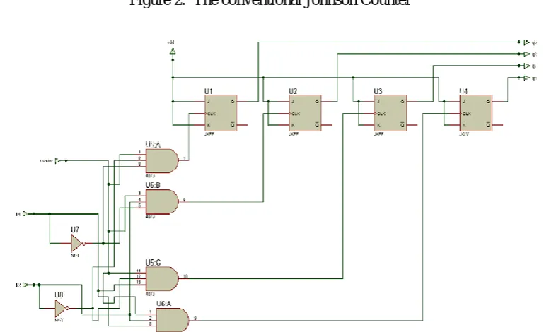
Figure 2. The conventional Johnson Counter
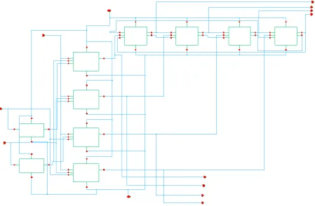
Figure 3. The proposed Johnson Counter with clock gating technique
[image:4.595.107.492.281.516.2]4
1234567890 ‘’“”
[image:5.595.81.525.120.300.2]International PostGraduate Conference on Applied Science & Physics 2017 IOP Publishing IOP Conf. Series: Journal of Physics: Conf. Series 1049 (2018) 012073 doi :10.1088/1742-6596/1049/1/012073
Figure 4. The schematic circuit of conventional Johnson counter
Figure 5. The schematic circuit of Johnson counter with clock gating
4. Result and Discussion
[image:5.595.84.534.340.634.2]1234567890 ‘’“”
[image:6.595.80.529.116.411.2]International PostGraduate Conference on Applied Science & Physics 2017 IOP Publishing IOP Conf. Series: Journal of Physics: Conf. Series 1049 (2018) 012073 doi :10.1088/1742-6596/1049/1/012073
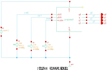
Figure 6. Test bench circuit
4.1 Transient Analysis
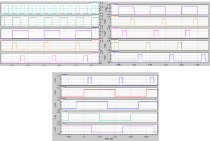
Figure 7 shows the simulation result of the conventional counter while Figure 8 shows the simulation result of the counter with clock gating circuit. It is shown that the counter with clock gating technique is getting a pulse when it is needed to toggle the output. Each flip flop is receiving a controlled clock sequence generated by the combinational logic circuit, master clock and the available masking clocks. Hence the power consumption of the system can be controlled efficiently. From the simulation, the power consumption for conventional Johnson Counter circuit is 67.09 µW while the power consumption for Johnson Counter with clock gating technique circuit is 21.22 µW. There is a reduction around 31% or about 45.87 µW when clock gating technique is used.
[image:6.595.161.438.560.732.2]6
1234567890 ‘’“”
[image:7.595.90.522.136.427.2]International PostGraduate Conference on Applied Science & Physics 2017 IOP Publishing IOP Conf. Series: Journal of Physics: Conf. Series 1049 (2018) 012073 doi :10.1088/1742-6596/1049/1/012073
Figure 8. Output waveform of Johnson Counter with clock gating
4.2 Design Rule Check and Layout versus SchematicTest
Design Rule Check (DRC) is a physical design process to determine if the circuit layout drawn, satisfies a number of rules as defined by the semiconductor manufacturer. Figure 9 shows the layout for the proposed design and the result of the DRC for the layout is successful. The total physical area for the proposed analog multiplier is 129 µm².
[image:7.595.97.497.564.736.2]1234567890 ‘’“”
International PostGraduate Conference on Applied Science & Physics 2017 IOP Publishing IOP Conf. Series: Journal of Physics: Conf. Series 1049 (2018) 012073 doi :10.1088/1742-6596/1049/1/012073
The layout versus schematic (LVS) is done to verify whether the layout really representing the schematic circuit. In this test, a comparisons between the layout and schematic is done to check the circuit connectivity. The result from the LVS test has shown the schematic and layout are equivalent.
5. Conclusion
A 4 bit Johnson Counter with a clock gating technique are designed in this project. The clock gating technique is used as a method to reduce the power consumption of the Johnson Counter. The circuit is designed utilizing 1.2 V power supply using Cadence EDA tools with 130 nm CMOS technology. The simulation result shown that the clock gating systems is effective in reducing the power consumption if Johnson Counter.
Acknowledgement
Special thanks to Nano Simulation Group (NanoSIM) and MiNT-SRC, Universiti Tun Hussien Onn Malaysia (UTHM) for providing the platform and the laboratory to conduct the research. This work was supported by Faculty of Electrical Engineering (FKEE), Universiti Tun Hussein Onn Malaysia (UTHM), Silterra and Collaborative Microelectronic Design Excellence Centre (CEDEC) for Innovate Malaysia Design Competition 2017.
References
[1] Sujatha B V and Venkateswarlu V T 2015 An efficient design for reduction of power dissipation in Johnson counter using clock gating International Journal of Science and Research4 2723 [2] Ismail S M, Rahman A B M S and Islam F T 2012 Low power design of Johnson counter using
clock gating IEEE 15th International Conference on Computer and Information Technology 510 [3] Ismail S M, Rahman S, Rahman M M and Ferdous N S 2012 A design scheme of toggle operation based Johnson counter with efficient clock gating. International Conference on Computational Intelligence, Modelling and Simulation 393
[4] Bansal E and Bajaj N 2016 A review on power efficient clock gated Johnson counter Imperial Journal of Interdisciplinary Research2 1284
[5] Pandey S, Uniyal S and Goel N 2015 An improved low power Johnson counter design with clock gating International Journal of Electronics and Communication Technology6 9
[6] Shelke M and Humane B 2015 Low power VLSI design using clock gating technique. International Journal of Advanced Research in Computer Engineering and Technology4 3270 [7] Wu Q, Pedram M and Wu X 2000 Clock gating and its application to low power design of
sequential circuits IEEE Transactions on Circuits and Systems 1: Fundamental Theory and Applications47 415
[8] Benini L and Micheli G D 1995 State assignment for low power dissipation IEEE Journal of Solid State Circuits30 258
[9] Pedram M, Wu Q and Wu X 1998 A new design of double edge triggered flip-flops Proceedings of ASP-DAC 417
![Figure 1. Clock gating technique [2]](https://thumb-us.123doks.com/thumbv2/123dok_us/8750758.891842/3.595.194.408.157.279/figure-clock-gating-technique.webp)