http://www.scirp.org/journal/opj ISSN Online: 2160-889X
ISSN Print: 2160-8881
The Effect of Nanometer Size Effect on the Optical
Property of Metallic Wire Grid
Yulun Wu1, Shimeng Feng2*
1School of Mechanical Engineering, Shanghai Jiao Tong University, Shanghai, China 2Physics Department of Shanghai Jiao Tong University, Shanghai, China
Abstract
We mainly investigated the effect of metallic wire grid on its optical property. At first, we give one simple model to deduce an expression which can describe the rela-tionship of the optical property with the width of metallic wire grid. This expression could be used to calculate the reflectance of the metallic wire grid. We also give the corresponding computer simulation. Our simulation shows that the reflectance would increase when the width of metallic wire grid increase. The wider the metallic wire grid is, the higher the reflectance is. The reflectance would reach the maximum value only when the width is over the free path of electronic.
Keywords
Metallic Wire Grid, Mean Free Path, Reflectivity
1. Introduction
The metallic wire grid has also been applied to a broad range of optical systems, such as WGPs, transparent metal electrodes for organic solar cells and organic light-emitting diodes. Now, many papers were focused on the investigation of the polarized property of metallic wire grid [1]-[7]. But few papers reported the theoretical optical property of metallic wire grid because the metallic wire grid always has large extinction coefficient. For example, Vadym Apalkov [8] studied the interaction between an H-wave and a thin metal film. They had calculated reflectance coefficients of a thin metal layer in the case of different values of the incidence angle. Utkin A. I. [9] analyzed the dependence of coefficients of transmission, reflection and absorption of an electromagnetic wave on the thickness of skin in thin metallic films layer. Latyshev A. V. [10] analyzed the
func-How to cite this paper: Wu, Y.L. and Feng, S.M. (2016) The Effect of Nanometer Size Effect on the Optical Property of Metallic Wire Grid. Optics and Photonics Journal, 6, 269-274.
http://dx.doi.org/10.4236/opj.2016.610027 Received: September 28, 2016
Accepted: October 24, 2016 Published: October 27, 2016 Copyright © 2016 by authors and Scientific Research Publishing Inc. This work is licensed under the Creative Commons Attribution International License (CC BY 4.0).
tions of transmission, reflection, and absorption coefficients with the angle of incidence of the electromagnetic wave, thickness of the layer. Then, these papers do not consider the effect of the width of metal film on these optical prompters
The optical property of the metal strongly depends on the free path of the free elec-tronic. In this paper, one simple model is given to investigate the effect of width of me-tallic wire grid on both the mean free path and the corresponding conductivity. Further, we also gave one relationship between the width of metallic wire grid and the reflectivi-ty. Finally, we give the theoretical simulation and discussions.
2. Theory
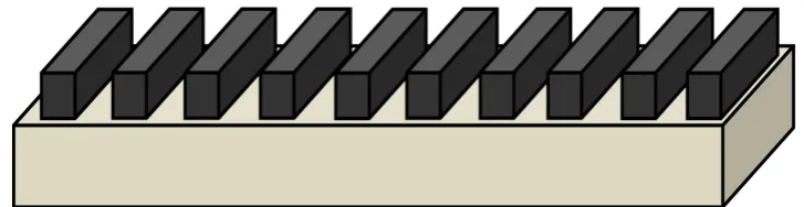
The structure model of one metallic wire grid is given in Figure 1, in which the metallic wire grid of cuboids with the same width and height are deposited on the glass sub-strates.
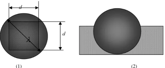
In order to study the effect of width on the electronic mean free path, we present one ball with the diameter of mean free path, in which the electronic can freely move Fig-ure 2 is a model when 2d<λ, λ is defined as the mean free path, d is the width and height of metallic wire grid, respectively. Figure 3 is another model when
2
d< <λ d . In Figure 2 and Figure 3, the overlapping region between the free path ball and metallic wire grid is the space where the electronic can freely move.
For the mean free path λ of electron in material, the volume of free path ball is that 3
4 π
3 2
V = λ
(1)
Here, λ is the mean free path in metallic media. For the model mentioned above, the volume of free path in metallic wire grid is, respectively,
3
3 2
2
3 2
2
5 2 4
2 2 1 π , 2
4 π 3 2
4 π 4π , 2
3 2 2 2 3 6
d d
V
d d
d d d
λ
λ λ
λ λ λ
λ λ
+ − − − ≤
′=
+ − − + < <
(2)
[image:2.595.191.555.593.687.2]Here, d is the width of wire grid. In order to the study the effect degree of the width of metallic wire grid on the mean free path, we define γ as one corrected factor. Thus, we have
(1) (2)
[image:3.595.243.508.226.338.2]Figure 2. The mode of free path affected by the width metallic wire grid ( 2d<λ). Here (1) is a front view, (2) is a lateral view.
Figure 3. The mode of free path affected by the width of metallic wire grid (d< <λ 2d). Here (1) is front view, (2) is a lateral view.
(
)
(
)
3 3 2 2 3 3 3 3 2 2 3 35 2 4
2 2 1 π
4 π 3 2
, 2
4 π
3 2
4 π 4π
3 2 2 2 3 6
, 2 4 π 3 2 d d V V d d d d d λ λ λ λ γ
λ λ λ
λ λ λ + − − − < ′ = = + − − + < < (3)
The substitution of (3) into (2) produces one expression to calculate the mean free path in wire grid, which is
( )
(
)
(
)
3 3 2 2 3 3 3 2 2 3 35 2 4
2 2 1 π
4 π 3 2
, 2
4 π
3 2
4 π 4π
3 2 2 2 3 6
, 2 4 π 3 2 d d d d d d d d λ λ
γλ λ λ
λ λ
λ λ λ
λ
γλ λ λ
λ + − − − = < = + − − +
= < <
Here, λ is the free path in material, λ
( )
d is the corrected mean free path in wiregrid.
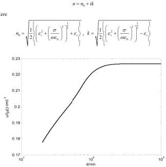
3. Calculation of Reflectance
Putting λ
( )
d into the conductivity formula of continuous metallic film, we have( )
( )
( )
1 3
1 1 exp exp
2 4
d d
p d
d d d
λ ζ
σ σ
λ λ
∞
= − + − − −
(5)
here σ∞ is the conductivity of normal metal material, σ is the conductivity of
corres-ponding metallic wire grid, ζ is related to the electron pen trance in length. For the metal (Ag) wire grid, the parameters ζ =0.025, p=0.5373,
0.226 cm
[image:4.595.209.534.360.687.2]σ∞ = µΩ , λ=40 nm, respectively. The simulation cure of (5) is given in
Figure 4.
Seeing from Figure 4, the conductivity increases as the width of metallic wire grid increases. For example, it is obvious that the conductivity at d=60 nm is larger than that at d=20 nm. Hence, we deduce that the conductivity depends on the width of metallic wire grid.
According to Maxwell’s equation, the relationship of refractive index with the con-ductivity is
0
n=n +ik (6) Here
1 2 2 2
0
0 1
2 r r
n ε σ ε
ωε
= + +
,
1 2 2 2
0 1
2 r r
k ε σ ε
ωε
= + −
here n0 is the real part of refractive index, k is the imaginary part. According to the reflectivity formulation, we have
(
)
(
)
2
1 1
2 2 2 2
2 2
0 0
2 2 0
2 2 2
1 1
0
2 2 2 2
2 2
0 0
1 1
1
2 2
1
1
1 1
1
2 2
r r r r
r r r
n k
R
n k
σ σ
ε ε ε ε
ωε ωε
σ σ
ε ε ε ε
ωε ωε
+ + − + + −
− +
= =
+ +
+ + + + + −
r
(7)
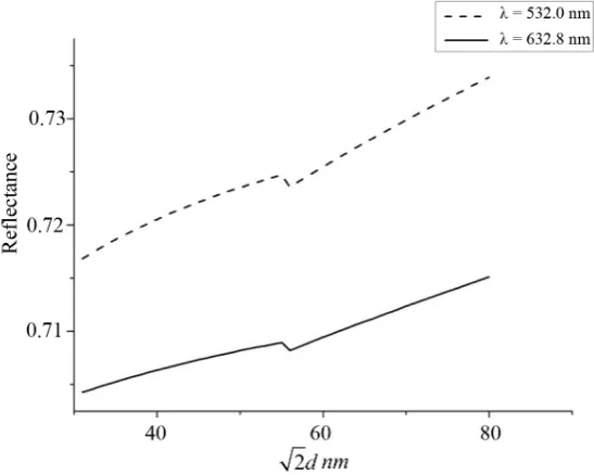
Equation (7) can clearly describe the relationship between the reflectance and with the width of metallic wire grid. It could be used to calculate the reflectance of wire grid. For example, When the light wavelength is equal to 632 nm and 532 nm, respectively, the corresponding relative dielectric constant of metal (Ag) ε = −r 15, 9.8− , respectively. For the wire grid of Ag, the parameters is ζ =0.025, p=0.5373, σ∞ =0.226 and
40 nm
λ= , respectively. Based on these parameters, we give the two cure (seeing Fig-ure 2), which corresponds to the reflectance of metallic wire grid at the wavelength of 532 nm and 632 nm, respectively. Because the material optical parameters of other wa-velength have not been obtained, we could not give the corresponding cure.
Seeing from Figure 5, the reflectance would increases when the width of metallic wire grid increases. For example, the reflectance is about 72% at 2d=40 nm, and the
reflectance of 73% at 2d =70 nm when the wavelength is 532 nm. For the
[image:5.595.200.552.109.218.2] [image:5.595.238.512.436.655.2]wave-length of 632 nm, the reflectance is about 69% at 2d=40 nm, and the reflectance of
71.5% at 2d=70 nm. These results demonstrate the reflectance is different when the
width of metallic wire grid is different.
4. Conclusion
This paper studied the influence of metal wire grid width on electron mean free path. The simple physical mode of electron mean free path affected by grid width is given. We give one corrected expression to calculate the conductivity of metallic wire grid. The theoretical simulation shows that the conductivity increases as the width of metal-lic wire grid increases. Further, we also investigated the relationship between the width of metal wire grid and the reflectance, and gave one corrected expression. Our simula-tion demonstrates that the reflectance increases as the width of metallic wire grid in-creases, which is very valuable to investigate the optical property of wire grid.
References
[1] Cincotti, G (2004) Polarization Gratings: Design and Applications. IEEE Journal of Quan-tum Electronics, 39, 1645-1652. http://dx.doi.org/10.1109/JQE.2003.819526
[2] Lohstroh, W., Felcher, G.P., Goyette, R., Munzenberg, M., Felsch, W., Lohstroh, W., Felch-er, G.P., Goyette, R., Munzenberg, M. and Felsch, W. (1999) Imprinted Spiral Structures as Neutron Polarizers. Physica B: Condensed Matter, 267, 352-354.
http://dx.doi.org/10.1016/S0921-4526(99)00025-3
[3] Schnabel, B., Kley, E. and Wyrowski, F. (1999) Study on Polarizing Visible Light by Subwa-velength-Period Metal-Stripe Gratings. Optical Engineering, 38, 220-226.
http://dx.doi.org/10.1117/1.602257
[4] Zeitner, U.D., Schnabel, B., Kley, E.B. and Wyrowski, F. (1999) Polarization Multiplexing of Diffractive Elements with Metal-Stripe Grating Pixels. Applied Optics, 38, 2177-2181.
http://dx.doi.org/10.1364/AO.38.002177
[5] Rennie, A.R. (2001) Comment on the Inverse Polarization Effect in Metal-Stripe Polarizers.
Journal of Optics A: Pure & Applied Optics, 3, 67-71(5).
[6] Clausnitzer, T., Kley, E.B., Tuennermann, A. and Zeitner, U.D. (2003) Polarizing Metal Stripe Gratings for a Micro-Optical Polarimeter. SPIE Proceedings, 5183, 8-15.
http://dx.doi.org/10.1117/12.507283
[7] Lazzaria, R., Jupillea, J. and Borenszteinb, Y. (1999) In Situ Study of a Thin Metal Film by Optical Means. Applied Surface Science, 142, 451-454.
http://dx.doi.org/10.1016/s0169-4332(98)00646-1
[8] Apalkov, V. and Stockman, M.I. (2013) Metal Nanofilm in Strong Ultrafast Optical Fields.
Physical Review B, 88, 245438. http://dx.doi.org/10.1103/PhysRevB.88.245438
[9] Utkin, A.I. and Yushkanov, A.A. (2014) The Effect of Reflectance Coefficients on the Inte-raction of an H Wave with a Thin Metal Film. Optics and Spectroscopy, 117, 632-635.
http://dx.doi.org/10.1134/S0030400X14090276
Submit or recommend next manuscript to SCIRP and we will provide best service for you:
Accepting pre-submission inquiries through Email, Facebook, LinkedIn, Twitter, etc. A wide selection of journals (inclusive of 9 subjects, more than 200 journals)
Providing 24-hour high-quality service User-friendly online submission system Fair and swift peer-review system
Efficient typesetting and proofreading procedure
Display of the result of downloads and visits, as well as the number of cited articles Maximum dissemination of your research work
Submit your manuscript at: http://papersubmission.scirp.org/