ISSN Online: 2327-4379 ISSN Print: 2327-4352
Designing Sensors Using Nano-Junctions
Vijay K. Lamba
1, O. P. Garg
21Global College of Engineering & Technology, Khanpur Khui, India 2RKSD College, Kaithal, India
Abstract
Nanowire field effect transistors can be modeled for ultrasensitive charge detection based bio- or chemical sensors. As critical dimensions of the nanowire sensor can be of the same order of size of biological molecules or chemical species yielding excep-tional sensing possibilities. In addition, the large surface/volume ratio will give high sensitivities simply because surface effects dominate over bulk properties. Thus, we modeled Si nanowire with different geometries in the different chemical environ-ment using NEGF approach. To analyze the performance, the sensitivity of Si nano-wire with different cross sections including circular, rectangular, and triangular is derived by two definitions. It is calculated that the sensitivity of Si nanowire with different structures is a function of geometrical parameters and doping density. It is illustrated that the sensitivity varies inversely with cross-section area, doping density, and also the length of nanowire.
Keywords
SINWs, Doping, NEGF, DFT
1. Introduction
In recent years, silicon nanostructures have attracted great interest as a building block for micro-electro-mechanical systems (MEMS), nano-electro-mechanical systems (NEMS) and nano-electronic devices. For example, silicon nanostructures find applica-tions in diverse areas such as sensors, bio-sensors, medical technology, and communi-cation technologies [1] [2]. Developing accurate and efficient models to predict the material properties of silicon nanostructures plays an important role in the design, characterization, and optimization of MEMS/NEMS and nano-electronic devices [3][4] [5][6]. Since the typical dimension of silicon nanostructures can vary from a few na-nometers to several hundred nana-nometers or even micrometers, the development of an How to cite this paper: Lamba, V.K. and
Garg, O.P. (2016) Designing Sensors Using Nano-Junctions. Journal of Applied Ma-thematics and Physics, 4, 2247-2253. http://dx.doi.org/10.4236/jamp.2016.412217
Received: September 23, 2016 Accepted: December 26, 2016 Published: December 29, 2016
Copyright © 2016 by authors and Scientific Research Publishing Inc. This work is licensed under the Creative Commons Attribution International License (CC BY 4.0).
appropriate model to accurately and efficiently predict the mechanical, and electrical response due to the external loadings and morphologies at different length scales is one of the main issues in a full device simulation of nanostructures.
Atomistic simulation methods such as first-principles quantum-mechanical methods
[7][8], molecular dynamics (MD) and Monte Carlo (MC) simulations [9][10] are gen-erally accurate for the analysis of nanostructures. However, the extremely high compu-tational cost prohibits the application of the atomistic methods at the device level. On the other hand, classical continuum theories which are based on continuum assump-tions are efficient and accurate at macroscopic scale, but they may not be directly ap-plicable for devices with nanometer features. To achieve the goal of accurately captur-ing the atomistic physics and yet retaincaptur-ing the efficiency at various length scales, mul-ti-scale modeling and simulation techniques have recently gained significant interest. So we used NEGF theory for Si nanowire with different geometries in the different chemical environment to analyze the performance, the sensitivity of Si nanowire with different cross sections.
In Section 2, we discuss the system model we used; Section 3 consists of NEGF-DFT formalism; in Section 4, we model the effect of encapsulation, & deformed structures, with results & conclusions in Section 5.
2. Model System
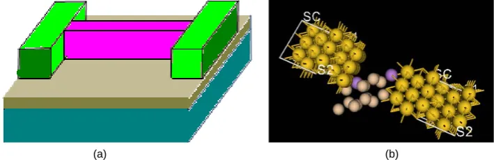
A general model for detecting molecules using Si-NWs is shown in Figure 1. The sys-tem consists of a Si-NW between two electrodes whose surface is functionalized. The electrodes are protected from the external environment by an oxide layer to avoid any undesired conductance change due to modification of electrode work function.
Due to the presence of native oxide on the NW surface, we assume that the negligible charge transfer is expected to take place between the molecule and the semiconductor. However, it is reported in [11] that the complimentary change in conductance for P-type and N-type doped NWs due to same organic molecules, which indicates that electrostatic interaction dominates the response. In this paper, we consider the analysis of sensitivity of Si nanowire with different cross sections only and neglect the effect of any surface states, as the response of a sensor is characterized in terms of its selectivity, settling time, and sensitivity.
[image:2.595.196.551.573.688.2]
(a) (b)
Selectivity denotes the ability of receptors to bind with the desired target in the pres-ence of various other (possibly similar) molecules and is entirely determined by the functionalization schemes [12]. The time taken by the sensor to produce a stable signal change defines the settling time, and is determined by molecule concentration, diffu-sion coefficients, and conjugation affinity to the receptor molecules [13]. Finally, sensi-tivity corresponds to the relative change in sensor characteristics upon attachment of target molecules on nanowire surface, which can be determined by the electrostatics of the system.
3. Theoretical Approach
The device model applied in the transport calculation consists of three parts, the stu-died material and two electrodes under bias Vb. Thus the Hamiltonian H for full sys-tems can be of the form:
ˆ ˆ ˆ ˆ ˆ ˆ
LL RR CC LC RC
H=H +H +H +H +H (1)
were HLL/RR are the Hamiltonian for left/right electrode and HCC + HLC + HRC gives
Ha-miltonian for extended molecule, consisting of molecule in addition to three layer of surface atoms of two electrodes. Here, each term is represented as
(
)
(
)
† † †
† † † †
, ,
, ,
, , ,
,
LL k k k k RR l l l l CC n n n n
LC k n k n k n n k RC l n l n l n n l
H c c H c c H c c
H V c c c c H V c c c c
ε ε ε
= = =
= + = +
∑
∑
∑
∑
∑
(2)were εi represents site energy of electron/hole positioned on I molecule, and
† ,
i i
c c
symbolize the creation andannihilation operator. As the definition of the current from the left electrode to the pinned system is
( )
d( )
[
]
, d
LL
L C LL
N t
I t e ie H N
t
→ = − = − (3)
Thus using
†
LL k k k
N =
∑
c c (4)we get
( )
†( ) ( )
†( ) ( )
, ,
L C k n k n k n n k
I → t = −ie
∑
V c t c t −c t c t (5)Combining green function we get
( )
, ,(
;)
(
;)
L C k n k n
I → t =e
∑
V G< nt kt −G< kt nt (6)Here G< stands for retarded green function defined as
( ) (
)
(
)
1Σ Σ
CC LC RC LL RR
G< E = E+iη I− H +H +H − − −
were iη and ΣLL RR( ) are an infinitesimal imaginary value and self energy elements
which includes influence of electrodes. For the steady state
( )
{
, ,( )
,}
2
Re 0
L C k n k n n k
e
I → t =
∑
V G< Similarly we calculate for ILL, IRR, ICC, ICR, etc. Thus
(
) ( )
( ) (
)
1,
ES−H G E =I G E = ES−H − (8)
Here S is the overlap matrix and I stands for identity operator. We describe overlap matrix is close to identity matrix, thus matrix calculation
† †
† †
0
0
LL LL LC LC LL LC LR
LC LC CC CC CR CR CL CC CR
CR CR RR RR RL RC RR
ES H ES H G G G
ES H ES H ES H G G G I
ES H ES H G G G
− −
− − − × =
− −
(9)
The solution of GCC is
( )
{
( )
( )
}
1CC CC CC L R
G E ES H E E
−
= − +
∑
+∑
(10)where,
∑
L( )
E , and∑
R( )
E are self energies corresponding with two leadsrespec-tively. The transmission probability is related to the Green function and can be de-scribed like
(
)
( )
( ) ( )
†( )
, b L CC R CC
T E V =TrΓ E G E Γ E G E (11)
( )
( )
( )
†, , ,
L R E i L R E L R E
Γ = −
∑
∑
(12)Tr means the trace analyzed. Thus using above equation we get transmission func-tion of the systems. The electron transport calculafunc-tions are performed using NEGF combined with DFT within the Landauer formalism [14] implemented in ATOMISTIX TOOLKIT [15]. The I-V characteristics are calculated by,
(
)
( )
( )
2 2
, b L R d
e
I T E V f E f E E
h
=
∫
− (13)where e, h, and fL(R) are electron charge, Planck’s constant, and the Fermi distribution functions at left (right) electrode, respectively. T(E, Vb) is the transmission coefficient at energy E and bias voltage Vb. We work with the Perdew-Zunger exchange and corre-lation functional [16] within the local density approximation. Norm-conserving pseudo potentials are used to describe the coreelectrons for all atoms. We have assumed the diameters SiNWs we used are less than 2 nm, Si-Si bond length is almost equal to bulk Si crystal. The nanowires we adopted had different cross section and in different sizes, and the surface is fully hydrogen terminated to eliminate the contribution of dangling bonds. We first of all calculated electronic band structures of SiNWs using ATOMISTIX TOOLKIT, which is excellently matched with experimental data [17][18][19].
4. Result & Conclusions
On analysis we found that with the increase in diameter of SiNWs the band gap de-creases and it is inversely proportional to the diameter of wire i.e.
( )
( )
1Bandgap
2 nm
eV r
From Figure 2, we find that gap width varied from 3.5 eV to 0.75 eV, for the varia-tion in cross secvaria-tion area from 0.5 nm2 to 1.5 nm2 for [110] [111] [112] series.
Our results are in agreements and perform the same trends with the experimental results [20]. Here, the size dependence indicates the quantum confinement, for the reason that the movement of electrons was confined in the plane perpendicular to wire axis. Energy band near Fermi energy level was effected since the diameter of wires is small, and the effective mass in confinement plane for [111] is smaller than that for [110] wire, and energy shift is large, which indicates the dependence of energy gap on orientation as well, but Figure 3 indicates slight dependence only.
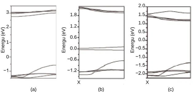
[image:5.595.246.500.315.463.2]As impurities and dopants are adsorbed on SiNW surface, so they influence the elec-tronic structure, which causes the change in conductance/transport properties. We calculate band structures for nanowires doped with N, & -OH using ATOMISTIX TOOLKIT. Interestingly, the different dopant adsorbed, clearly resulted in different band structure. Thus, all the results shown in Figure 4 are evidence that the different adsorbents modify the band structures in different ways so, we can use SiNWs as
Figure 2. Band gap of the SiNWs versus the cross-sectional diameter, blue dots is for [110], brown for [111], and green for experimental da-ta da-taken from reference [17] for [111].
Figure 3. Band gap of the SiNWs versus the cross-sectional area, blue dots is for [111], brown for [112].
0.5 1 1.5 2 2.5 3 3.5
0 1 2 3 4 5 6 7 8 9
Ener
gy
gap(
eV
)
Diameter(nm)
[110] [111]
[111] Expt [12]
1.3 1.8 2.3 2.8 3.3
0 0.5 1 1.5 2 2.5
Ener
gy
gap (
eV
)
Cross section area (nm2)
[image:5.595.246.503.527.674.2](a) (b) (c)
Figure 4. Diagram for electronic band structure (a) SiNW, (b) SiNW with N doped, (c) SiNW with -OH group.
sensors by tuning the band gaps through controlling surface density of dopants/surface treatments.
References
[1] Cui, Y. and Lieber, C.M. (2001) Functional Nanoscale Electronic Devices Assembled Using Silicon Nanowire Building Blocks. Science, 291, 851-853.
https://doi.org/10.1126/science.291.5505.851
[2] Craighead, H.G. (2000) Nanoelectromechanical Systems. Science, 290, 1532-1535.
https://doi.org/10.1126/science.290.5496.1532
[3] Paulose, M., Grimes, C.A. Varghese, O.K. and Dickey, E.C. (2002) Self-Assembled Fabrica-tion of Aluminum-Silicon Nanowire Networks. Applied Physics Letters, 81, 153-155.
https://doi.org/10.1063/1.1492005
[4] Dequesnes, M., Rotkin, S. and Aluru, N.R. (2002) Calculation of Pull-In Voltagesfor Car-bon-Nano-Tube-Based Nano-Electro-Mechanical Switches. Nanotechnology, 13, 120-131. [5] Tang, Z., Xu, Y., Li, G. and Aluru, N.R. (2005) Physical Models for Coupled
Electrome-chanical Analysis of Silicon Nano-Electro-MeElectrome-chanical Systems.Journal of Applied Physics, 97, 114304. https://doi.org/10.1063/1.1897483
[6] Tadmor, E.B., Ortiz, M. and Philips, R. (1995) Quasicontinuum Analysis of Defects in Sol-ids. Philosophical Magazine A, 73, 1529-1563. https://doi.org/10.1080/01418619608243000
[7] Tang, Z. and Aluru, N.R. (2008) Multiscale Mechanical Analysis of Silicon Nanostructures by Combined Finite Temperature Models. Computer Methods in Applied Mechanics and Engineering, 197, 3215-3224. https://doi.org/10.1016/j.cma.2007.11.018
[8] Tang, Z., Zhao, H., Li, G. and Aluru, N.R. (2006) Finite-Temperature Quasi-Continuum Method for Multiscale Analysis of Silicon Nanostructures. Physical Review B, 74, Article ID: 064110. https://doi.org/10.1103/PhysRevB.74.064110
[9] Medic (2003) Two Dimensional Device Simulation Program, 2003. Synopsis, Version 2003. [10] Nair, P.R. and Alam, M.A. (2006) Simulation of Nanowire Bio Sensors. Proceedings of 64th
Device Research Conference, 183-184.https://doi.org/10.1109/DRC.2006.305048
[11] Nogueira, F., Castro, A. and Marques, M.A.L. (2003) A Tutorial on Density Functional Theory. In: Fiolhais, C., Nogueira, F. and Marques, M.A.L., Eds., A Primer in Density Functional Theory, Springer, Berlin, 218-256.
[12] Stern, E., Klemic, J.F., Routenberg, D.A., Wyrembak, P.N., Turner-Evans, D.B., Hamilton,
X X
−1.2 −0.6 0.0 0.6 1.2 1.8
−2.0 −1.5 −1.0 −0.5 0.0 0.5 1.0 1.5 2.0
−1 0 1 2 3
E
ner
gu
(eV
)
E
ner
gu
(eV
)
E
ner
gu
(eV
A.D., LaVan, D.A., Fahmy, T.M. and Reed, M.A., (2007) Label-Free Immunodetection with CMOS-Compatible Semiconducting Nanowires. Nature, 445, 519-523.
https://doi.org/10.1038/nature05498
[13] Wang, J., Palecek, D., Nielsen, P.E., Rivas, G., Cai, X., Shiraishi, H., Dontha, N., Luo, D. and Farias, P.A.M. (1996) Peptide Nucleic Acid Probes for Sequence-Specific DNA Biosensors.
Journal of the American Chemical Society, 118, 7667-7670.
https://doi.org/10.1021/ja9608050
[14] Nair, P.R. and Alam, M.A. (2006) Performance Limits of Nanobiosensors. Applied Physics Letters, 88, Article ID: 233120.
[15] Datta, S. (1995) Electronic Transport in Mesoscopic Systems. Cambridge University Press, Cambridge.https://doi.org/10.1017/CBO9780511805776
[16] AtomistixToolKit Version 2.0. Atomistix A/S. www.atomistix.com
[17] Gonze, X., Beuken, J.M., Caracas, R., Detraux, F., Fuchs, M., Rignanese, G.-M., Sindic, L., Verstaete, M., Zerah, G., Jollet, F., Torrent, M., Roy, A., Mikami, M. and Allen, D.C. (2002) First-Principles Computation of Material Properties: The ABINIT Software Project. Com-putational Materials Science, 25, 478-492.https://doi.org/10.1016/S0927-0256(02)00325-7
[18] Perdew, J.P. and Zunger, A. (1981) Self-Interaction Correction to Density-Functional Ap-proximations for Many-Electron Systems. Physical Review B, 23, 5048-5079.
https://doi.org/10.1103/PhysRevB.23.5048
[19] Li, C.P., Lee, C.S., Ma, X.L., Wang, N., Zhang, R.Q. and Lee, S.T. (2003) Growth Direction and Cross-Sectional Study of Silicon Nanowires. Advanced Materials, 15, 607-609.
https://doi.org/10.1002/adma.200304409
[20] Li, D., Wu, Y., Kim, P., Shi, L., Yang, P. and Majumdar, A. (2003) Thermal Conductivity of Individual Silicon Nanowires. Applied Physics Letters,83, 2934-2936.
https://doi.org/10.1063/1.1616981
Submit or recommend next manuscript to SCIRP and we will provide best service for you:
Accepting pre-submission inquiries through Email, Facebook, LinkedIn, Twitter, etc. A wide selection of journals (inclusive of 9 subjects, more than 200 journals)
Providing 24-hour high-quality service User-friendly online submission system Fair and swift peer-review system
Efficient typesetting and proofreading procedure
Display of the result of downloads and visits, as well as the number of cited articles Maximum dissemination of your research work
![Figure 2. Band gap of the SiNWs versus the cross-sectional diameter, ta taken from reference blue dots is for [110], brown for [111], and green for experimental da-[17] for [111]](https://thumb-us.123doks.com/thumbv2/123dok_us/7792286.726416/5.595.246.503.527.674/figure-sinws-versus-sectional-diameter-reference-green-experimental.webp)