2016 International Congress on Computation Algorithms in Engineering (ICCAE 2016) ISBN: 978-1-60595-386-1
1 INTRODUCTION
Because of the prevalence of the intermittent problems, the volatility and the problem that output voltage level is low in new renewable energy, the traditional bridge inverters are unable to get good performance on these occasions because of inherent disadvantages. Z-source inverter has emerged as the solution for problems, and traditional inverters have been applied on these occa-sions. Z-source inverter allows the two switch tubes on the same bridge arm shoot, inverter bridge and impedance network coupling to provide a new mecha-nism to achieve up/down inverter, so it has broad ap-plication prospects in new energy generation, fre-quency control system and other occasions.
Compared with traditional bridge inverter, Z-source inverter is increased in an X-type impedance network. Therefore, it is very important to model Z-source im-pedance network accurately in system’s dynamic per-formance analysis, and domestic and foreign scholars have already proposed a variety of modeling methods on impedance network.
[3-6] had a study on Z-source inverter based on steady-state circuit model and constructed a simplified
circuit model for Z-source inverter. The model can only analyze quiescent operating point of the system, it is unable to get the small-signal model of the system and cannot possess frequency domain characteristics and transfer function of the system variables to guide the design of the controller. [7] used the state-space averaging method for Z-source inverter modeling and designed the controller based on the model, but this model only analyzes the transfer function of the shoot through the duty cycle to capacitor voltage and has no comprehensive analysis of the effect on inductor pa-rameters, and capacitor parameters may have on dy-namic performance; [8] used the state-space averaging method and built a small-signal model for Z-source inverter with a continuous conduction mode. This model introduces dynamic characteristic of capacitor and inductor in the impedance network, expands the steady-state model and gives the small-signal equiva-lent circuit. This paper uses Bode diagram to analyze the impact of inductor and capacitor parameters on the system dynamic performance, while this model does not consider the parasitic parameters of inductor and capacitor within a certain frequency range, and the accuracy of the model is not enough, so it is unable to make the affect parameters possess the dynamic per-formance of DC link voltage; [9] respectively used the
Optimization Design of Parameters of Z-source Inverter based on
the Small-signal Model using State-space Averaging Method
Houyun Liu1, Tao Sun2*, Shiying Hou2, Zhicheng Guo2, Ruimiao Wang1 & Ruilin Xu1 1
Electric Power Research Institute, State Grid Chongqing Electric Power Company, Chongqing, China 2
State Key Laboratory of Power Transmission Equipment & System Security and New Technology, Chongqing University, Chongqing, China
ABSTRACT: Optimization of inverter’s parameters is one of the key issues in improving the inverter’s per-formance. Z-source inverter is a new kind of topological structure. The research on optimization of its impedance network’s Parameters is of great value in theory and application. First, the state-space averaging method is used to establish the small-signal model of impedance network capacitor voltage and obtain the transfer function from the direct duty cycle to the impedance network capacitor voltage. And the influence of inductor and capacitor’s parameters changes on dynamic performance of capacitor voltage’s step response is analyzed based on this. At the same time, the optimized principle of impedance network’s parameters is proposed. Finally, the validity of the proposed optimized principle is proved by the simulation results.
Keywords: Z-source inverter; state-space averaging method; small-signal model; parameter optimization
small-signal analysis and the signal flow diagram analysis method to get transfer function of shoot through the duty cycle to the capacitor voltage and the input voltage to the capacitor voltage, and used the root locus analysis method to analyze the impact of shoot through duty cycle, inductor, capacitor and their parasitic parameters on capacitor voltage stability; [10] used the signal-flow diagram modeling method to obtain dynamic small-signal model of Z-source im-pedance network, considering parasitic parameters of components, and the transfer function of shoot through duty cycle to capacitor voltage reveals the existence of right–half-plane zero point and used the classical root locus method to analyze the influence of component parameters on the dynamic performance of the system; [11] respectively modeled the Z-source impedance network and the inverter bridge, obtained the state-space model of Z-source inverter and com-pleted the design of a closed-loop controller; [12] given the mathematical model of three-phase inverter bridge described by both switching function and duty cycle and designed the control system guided by the mathematical model described by duty cycle.
Currently, the modeling and analysis of Z-source impedance network is always conducted to analyze network parameters on the system dynamic and static performance, so how to determine the selection prin-ciple of parameters and optimize impedance network parameters ranges based on the analysis about the intrinsic characteristics of the impedance network is still key issue to be solved.
For existing problems in Z-source inverter imped-ance network modeling studies, in this paper we use the state-space averaging method to establish a small-signal model of impedance network capacitor voltage for the transfer function of shoot through duty cycle, using classical control theory root locus method to analyze the effects that network inductor, capacitor and parasitic capacitor as well as shoot through duty cycle have on the capacitor voltage dynamic perfor-mance. Then we research on the optimization of the impedance network parameters in the model based on the verification of correctness of the small-signal model of capacitor voltage. By comparing the step response of Z-source inverter circuit simulation and the small-signal model of capacitor voltage when duty cycle is under mutation, we verified the correctness of the model; on this basis, inductor and capacitor pa-rameters were optimized to provide a theoretical guidance for the design of the impedance network parameters, according to the effect that the impedance network parameters have on the capacitor voltage dynamic performance of the step response.
2 STATE-SPACE AVERAGING SMALL-SIGNAL
MODEL OF Z-SOURCE INVERTER
[image:2.516.297.423.174.267.2] [image:2.516.265.451.459.604.2]The general topology of Z-source inverter is shown in
Figure 1. This topology is built on the introduction of a X-type two-port network based on a conventional voltage-source inverter, and DC input power source and the main circuit of the inverter bridge coupled together through the network, thus ensuring that the Z-source inverter can operate under the conditionthe conventional voltage-source inverter operated in while working in shoot through a state the tradition inverter prohibited, on which state the inverter bridge provides a unique up/down function [13].
VL1
+
-Vin
+
-VL2+ -+
VC1
-+
V
C2
-iL1
iL2 Vdc
Din
iin
Figure 1. The topology equivalent circuit of Z-source inverter.
When building a small-signal model of impedance network, we need to consider the parasitic resistances
1
r and r2of the network inductor and the capacitor
equivalent series resistances R1 and R2. For the convenience of analysis, the impedance network takes a symmetrical structure, so
1 2 1 2
C C C L, L L,
1 2 1 2
r r r,R R R. Choose the impedance net-work inductor current and capacitor voltage as the state-space average model state variables. When the diode Din is off, Z-source inverter will be in through state, and the state-space equation of direct connection can be shown as follows:
1
1 1
1
2 2
2
2
1
0 0
1
0 0 0
1
0 0
1
0 0 0
0 0
0 0
0 0
0 0
L
L C
C
L L
C
C
in
in
di r R
dt L L
i dV
V
dt C
di r R i
L L
dt V
dV
C dt
V
i
(1)
cor-responding state-space equation can be shown as fol-lows: 1 1 1 1 2 2 2 2 1 0 0 1
0 0 0
1
0 0
1
0 0 0
1 1 0 1 1 0 L L C C L L C C in in
di r R
dt L L
i dV
V
dt C
di r R i
L L dt V dV C dt R L L V C R i L L C (2)
According to the mind of state-space averaging, and in order to establish piecewise-linear equations based on the circuit continuum model with different switch-ing states and get the state equation of the circuit in the whole switching cycle, we need to segment the above equation and make them be averaged. As the selected state variables, input variables and output variables of straight-through state and non-through-state are the same, so the averaging equa-tion can be obtained by the weighted average of the coefficient matrix. Here, we take shoot through duty cycle D0, so the non-pass-through duty cycle is 1-D0. And the state averaging equation can be obtained ac-cording to the state averaging method.
in in C L C L C L C L i V C L R L C L R L D V i V i C D C D L D L R r L D C D C D L D L D L R r dt dV dt di dt dV dt di 1 0 1 1 0 1 ) 1 ( 0 0 1 ) ( 1 0 0 1 0 1 0 ) ( 0 0 0 0 0 0 0 0 0 2 2 1 1 2 2 1 1 (3)
Based on the symmetry of the impedance network, we can obtain:
1 2 1 2
C C C L L L
V
V
V
,
i
i
i
The original four-order equation reduces to
two-order equation as follows:
0 0 0 1 2 ( ) 1 2 0 1 (1 ) 1 0 L L c C in in
di r R D
i
dt L L
D dV V C dt R V L L D i C (4)
According to the inductor volt-second balance and capacitor charge balance, we can get static working point for steady state:
0
0
0 0 0
2
0 0
1 1 2
1 (1 )[(1 2 ) ( )]
1 2 (1 2 )
L in
C in in
D
i i
D
D D D R r R
V V i
D D (5)
In order to solve the dynamic transfer function of the system, we introduce the disturbance quantity of stable operating point to obtain the state variable
which contains disturbance quantity:
ˆ
,
ˆ
,
ˆ
,
ˆ
L L C c in in in in
i
i
V
v V
v
i
i
andD
d
ˆ
.Defined matrix:
1
2
1
2
( ) / 1/
1/ 0
( ) / 1/
1/ 0
0
1/ /
0 1/
r R L L
A
C
r R L L
A
C B
L R L
B C
Make AD A0 1 (1 D A0) 2,BD B0 1 (1 D B0) 2, L C i X V , in in V U i
,we can get linear dynamic equation of small-signal model of impedance network.
1 2 1 2
ˆ / ˆ ˆ
ˆ
ˆ / ˆ
ˆ ( ) ( ) in L L in C C v
di dt i
A B
i
dV dt V
A A X B B U d
(6)
Take the Laplace transform of (6) at both ends, it is shown as follows:
1 2 1 2
ˆ( ) ˆ( )
ˆ
( ) ( ) ( )
sE A x s Bu s
A A X B B U d s
( )
(7)
ˆ
ˆ ( )
ˆ( ) ˆ ˆ( ) ˆ
( ) ( )
L in
C in
i s V s
x s u s
V s i s
( )
, By (7) we can get
1
1 2 1 2
0 0 0
0 0
ˆ ˆ( ) { ˆ( ) ( ) ( ) ( )}
1 2 1 (1 ) 2
ˆ
ˆ( ) ˆ
1 2 1 ( ) 2
0 ( ) ( )
C in in in
in L in
x s sE A Bu s A A X B B U d s
D D D R V V Ri
s v s
LC L L L L d s
D Ls R r D i i
Q i s
C L C C
(8)
Where: 2 2
0
( ) (1 2 )
QLCs R r Cs D .
There-fore, the small-signal inductor current of Z-source network is shown as follows:
) ( ˆ ) 2 )( 2 1 ( ) 2 ( ) ( ˆ )] 2 1 ( )[ 2 1 ( ) ( ˆ ) 1 ( ) ( ˆ 0 0 0 0 s d Q i i D s C Ri V V s i Q D s C R D s V Q s C D s i L in in in C in in L (9)
The small-signal capacitor voltage of Z-source network is shown as follows:
) ( ˆ ) 2 )( ( ) 2 )( 2 1 ( ) ( ˆ )] ( ) 2 1 )[( 1 ( ) ( ˆ ) 2 1 )( 1 ( ) ( ˆ 1 0 0 0 0 0 s d Q i i r R Ls Ri V V D s i Q r R Ls R D D s V Q D D s V L in in in C in in C (10)
In (10), make ˆ ( ) 0 ˆ( ) 0
in in
V s ,i s , and the transfer function of capacitor voltage to shoot through the duty cycle of Z-source network can be shown as follows:
0
2 2
0
ˆ ( ) (1 2 )(2 ) ( )( 2 )
( ) ˆ
( ) (1 2 )
( )
C C in in in L
VD
V s D V V Ri Ls R r i i
G s
LCs R r Cs D
d s
(11)
3 VERIFY THE SMALL-SIGNAL MODEL IMPEDANCE NETWORK
Z-source inverter works by adjusting the shoot through the duty cycle to achieve the DC link Boost, so it has some impacts on system performance. Meanwhile, in order to maintain a stable inverter bridge, DC link voltage needs to be achieved by con-trolling the Z-source capacitor voltage to be stable. By (11) we can see that the transfer function of capacitor voltage to shoot through the duty cycle has right half-plane zero, it leads to the phenomenon that the transient response of Z-source network will appear in a non-minimum phase. Therefore, we need to verify the correctness of the model at first in order to opti-mize the dynamic characteristics of the system by parameters.
In order to observe whether the results of both two are the same, we compare the voltage dynamic re-sponse of linear small-signal model and dynamic sim-ulation results of the actual circuit capacitor voltage.
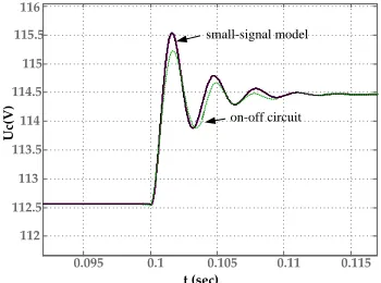
Simulation parameters of Z-source impedance net-work are shown as follows: L1=L2=1mH, C1=C2=1000μF,Vin100V , fs 10kHz , RL30Ω. We use simple boost control mode. In this process, the shoot through the duty cycle is changed from 0.1 to
0.11 at 0.1s. Figure 2 is the step response of simula-tion circuit of Z-source impedance network and small-signal model of capacitor voltage. As can be seen from the figure, small-signal model is under the disturbancedˆ0.01, its step response is consistent with the output of switch electronic circuit. It can show that the small-signal linear model of shoot through the duty cycle to capacitor voltage is valid. It can accurately reflect the internal dynamic character-istics of Z-source inverter impedance network.
0.095 0.1 0.105 0.11 0.115
[image:4.516.276.451.170.300.2]112 112.5 113 113.5 114 114.5 115 115.5 116 t (sec) U c( V ) small-signal model on-off circuit
Figure 2. The output response of capacitor voltage when D0 varies 0.01.
0.09 0.095 0.1 0.105 0.11 0.115 0.12 0.125 112 112.5 113 113.5 114 114.5 115 115.5
Linear Simulation Results
Time (sec) A m p li tu d e
C=1000μF
0.099 0.0995 0.1 0.1005 0.101 13.9 14 14.1 14.2 14.3 14.4 14.5 14.6 14.7 14.8
Linear Simulation Results
Time (sec)
A
m
plitu
de
L=300μH L=600μH
[image:4.516.268.458.347.501.2]L=900μH
Figure 3. The step response of capacitor voltage when inductance parameter varies.
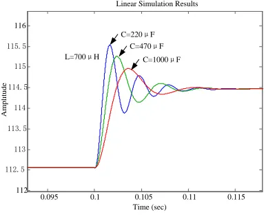
0.15 when t=0.1s. As can be seen from the figure, the capacitor voltage increases volatility as the inductance increases. At the same time, both the rise time and the settling time increase, the negative impulse caused by the non-minimum phase also will be intensified.
Similarly, Figure 4 is capacitor voltage step re-sponse curve when the duty cycle is mutated at t=0.1s and the need of different capacitor values in the ripple range is met. (11) shows that the system damping is increased with the increase of the capacitor value, but system zero has no relationship with capacitor value, which means that the change of capacitor value has no effect on the non-minimum phase characteristics of the system. It can be clearly seen from Figure 4 that, with the increasing value of capacitor, the rising time of the system is increased at the same time. The in-crease of system damping reduces the overshoot of the system to a certain extent.
0.095 0.1 0.105 0.11 0.115 112
112.5 113 113.5 114 114.5 115 115.5
116
Linear Simulation Results
Time (sec)
A
m
p
li
tu
d
e
L=700μH
C=220μF C=470μF
[image:5.516.55.248.253.409.2]C=1000μF
Figure 4. The step response of capacitor voltage when capacitor parameter varies.
4 THE IMPEDANCE NETWORK PARAMETER
OPTIMIZATION
From the previous analysis, we know the selection of impedance network capacitor, and inductor parameters have a direct influence on the dynamic characteristics of the capacitor voltage. Therefore, in order to obtain the desired capacitor voltage dynamic characteristics and to ensure the stability of DC voltage, we can get a stable output waveform of the inverter bridge and we need to optimize the value of inductor and capacitor. However, selecting the optimal parameter values is determined based on several conditions of general restrictions, so we should consider the following crite-ria at first:
(1) A suitable damping factor and an appropriate quality factor.
(2) Consider both power density and economic condition and meet ripple requirement based on the components of inductor and capacitor as smallest as possible.
(3) Make sure that the closed-loop system has suffi-cient bandwidth.
(4) The resonant frequency of the system should try to stay away from the switching frequency of the in-verter bridge.
(5) Effect of non-minimum phase characteristic. In addition to the above principles, we need to con-sider a non-work state of Z-source inverter caused by improper impedance network parameters, which is discontinuous inductor current mode. Therefore, we need to consider the basis of the above constraints on the parameters of the impedance network optimization research.
When we design the network parameters, the influ-ence of Z-source inverter non-work state on the per-formance of the inverter output needs to be considered in the optimization of inductor parameters. And such non-work state can be avoided by selecting the induc-tor value appropriately. Therefore, we should first consider the critical inductor value of Z-source invert-er discontinuous mode and provide a refinvert-erence for selecting the optimal parameters.
To avoid discontinuous current mode, there is a need to meet:
2 2
max min
in L L L
i i I
i (12)
According to Z-source inverter operation principle, when in pass-through state, the diode is turned off, and the capacitor voltage
u
Cand inductor voltageu
L network are equal. At this point, the impedance net-work inductor current ripple
i
L is:
DTs C C s
L
L T D u dt L u
i 0
0
0
(13)
The maximum iinmax of the inverter bridge input side DC link current and the valid value ILf of the
inverter output side currents satisfy:
max
2
in Lf
i
I
(14) From the above equation, we can get that the in-ductor value range in continuous inin-ductor current mode is:Lf L
s C
I I
T D u L
2 2
0
(15)
pole. So if the inductor value is too large, it will in-crease the negative impulse the non-minimum phase phenomena brings, and the selection of inductor pa-rameter is 700μH.
Figure 5 shows that the capacitor parameters have effect on the system step response. The increasing capacitor value will increase the system damping, making the system response more stable. When the capacitor value is more than 1000μF, it will have little impact on overshoot system. Therefore, in order to take both system damping factor and quality factor into account, we select the capacitor parameters which are 1000μF. With these parameters, the system trans-fer function open loop gain is 20dB and the resonant frequency is 190Hz, which meet the system’s design specifications.
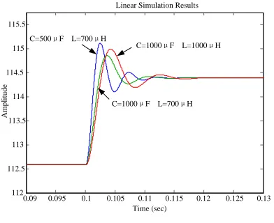
In order to verify the above capacitor, the inductor parameter is a relatively good choice. We select three sets of approaching data to compare based on this parameter. Three sets of control data values are shown as follows: 1) capacitor (500μF) and inductor (700μH); 2) capacitor (1000μF) and inductor (1000μH); 3) ca-pacitor (1000μF) and inductor (700μH).
Based on these three sets of data, we can get the re-sponse curves of capacitance voltage under different parameters in Figure 5. As can be seen from the figure, we can find by comparison as follows: The response curve of capacitor (1000μF) and inductor (700μH) is relatively good, the overshoot is relatively small, and the adjustment time is relatively short. Therefore, the principle of optimization parameters selection pro-vides a strong theoretical support.
0.09 0.095 0.1 0.105 0.11 0.115 0.12 0.125 0.13 112
112.5 113 113.5 114 114.5 115 115.5
Linear Simulation Results
Time (sec)
A
m
p
li
tu
d
e
C=500μF L=700μH
C=1000μF L=1000μH
[image:6.516.57.253.395.555.2]C=1000μF L=700μH
Figure 5. The response curves of capacitance voltage under different parameters.
5 CONCLUSION
In this paper, we construct a small-signal model-based Z source inverter based on the state-space averaging method, and obtain the transfer function of impedance network capacitor voltage to shoot through the duty cycle by the model. By comparing the output of the
impedance network emulation circuit and the step re- sponse of the capacitor voltage small-signal model in case that the duty cycle changes suddenly, we verified the correctness of the model; on this basis, wedefined the optimization of the impedance network inductor and the capacitor parameter selection principle ac-cording to the effect of impedance network passive components parameters changing on the dynamic performance of capacitor voltage step response; final-ly, the simulation results demonstrate that the princi-ple of optimization parameters is feasible. And the conduction of the small-signal model and the optimal selection method in this paper will lay a theoretical foundation for further work to improve the perfor-mance of Z-source inverter.
REFERENCES
[1] Fang Zheng Peng. 2003. Z-Source Inverter. IEEE Transactions on Industry Applications, 39(2): 504-510. [2] Fang Zheng Peng., Xu Peng Fang, Bin Gu, Qi Gao, &
Zhao Ming Qian. 2004. Z-Source Converter. Transac-tions of China Electrotechnical Society, 19(2): 47-51. [3] Gayathri Murthi, & Olorunfemi Ojo, 2007. A
Compre-hensive Analysis of a Three-Phase Z-Source DC-AC Converter. Applied Power Electronics Conference: 1714-1720.
[4] Fang Zheng Peng, Miaosen Shen, & Zhaoming Qian. 2005. Maximum boost control of the Z-source inverter.
IEEE Transactions on Power Electronics,20(4):
833-838.
[5] Fang Zheng Peng, Joseph A., Jin Wang, & Miaosen Shen, 2005. Z-source inverter for motor drives. IEEE
Transactions on Power Electronics, 20(4): 857-863.
[6] Poh Chiang Loh, & D.M. Vilathgamuwa,m et al. 2004. Pulse-width modulation of Z-source inverters. IEEE
Transactions on Power Electronics, 20(6): 1346-1355.
[7] Miaosen Shen, Qingsong Tang, & Fangzheng Peng, 2007. Modeling and controller design of the Z-source inverter with inductive load. Power Electronics Special-ists Conference: 1804- 1809.
[8] Jingbo Liu, Jiangang Hu, & Longya Xu. 2005. A Modi-fied Space Vector PWM for Z-Source Inverter -Modeling and Design. Proceedings of the Eighth Inter-national Conference on Electrical Machines and Sys-tems, 2: 1242-1247.
[9] P.C. Loh, D.M. Vilathgamuwa, & C.J. Gajanayake, et al. 2005. Transient modeling and analysis of pulse-width modulated Z-source inverter. Industry Applications
Conference, 4: 2782-2789.
[10] C.J. Gajanayake, D.M. Vilathgamuwa, & Poh Chiang Loh. 2005. Small-Signal and Signal-Flow-Graph Mod-eling of Switched Z-Source Impedance Network. Power Electronics Letters, 3(3): 111-116.
[11] Xiaogao Chen, & Qing Fu, D. Infield, et al. 2009. Mod-eling and Control of Z-Source Grid-connected PV Sys-tem with APF Function. IEEE UPEC: 1-5.
[12] Jing Zhang. 2010. Research on Z Source Inverter Con-trol and Application. Shandong University Master’s Thesis.