United States Patent
[19]Lipcon
[54] PRECISION SETTING OF CURRENTS AND REFERENCE VOLTAGES
[75] Inventor: Jesse B. Lipcon, Harvard, Mass.
[73] Assignee: Digital Equipment Corporation, Maynard, Mass.
[21]
[22]
[63]
[51]
[52]
[58]
[56]
Appl. No.: 292,006
Filed: Aug. 11, 1981
Related U.S. Application Data
Continuation-in-part of Ser. No. 267,394, May 26, 1981, Pat. No. 4,384,363.
Int. CI.3 ... H04B 1/00; H04B 1/40 U.S. CI ... 455/58; 323/281; 363/21 Field of Search ... 323/224, 265, 267, 268, 323/273,275, 281, 312; 363/21; 455/78, 58
References Cited
U.S. PATENT DOCUMENTS
3,399,339 8/1968 Yeager ... 3231273
FOREIGN PATENT DOCUMENTS
694853 10/1979 U.S.S.R ... 323/281
OTHER PUBLICATIONS
Electronic Design, vol. 13, No.9, pp. 44, 45, Apr. 26,
1965.
+94V to15.75V
74
DCtoDC
CONVERTER
358
78 362
75
[11]
[45]
4,412,347
Oct. 25, 1983
Rev. Sci. Instr., vol. 42, No.
to,
pp. 1532, 1533, Oct. 1971.Primary Examiner-William H. Beha, Jr. Attorney, Agent, or Firm-Cesari and McKenna
[57] ABSTRACT
A precision voltage and current source for use, for example, in a transceiver for a carrier-sense multiple access communications network using collision detec-tion wherein the use of one or more precise threshold voltages is required. The threshold voltage(s) is (are) created by a current source which pulls a current through a precise resistive load to yield a precise volt-age. A power supply with regulated voltage drives the current source. A feedback voltage from the current source, proportional to the output current of the source, is compared with a reference zener diode voltage; the difference, or error, voltage controls the regulator to drive the regulated power supply voltage in the direc-tion which drives the error voltage to zero. The precise resistive load is preferably formed of two resistors in series. A first threshold voltage is developed across one resistor, corresponding to the average signal level re-quired for receiving signals on the network. A second threshold voltage is developed across the series pair of resistors, corresponding to the minimum average signal level which would be produced by a collision.
4 Claims, 10 Drawing Figures
}
THRESHOLD VOLTAGES
12A
12B ...
1 --+-~14
r
-1
28 - - - ,
1
26
25
II
I
I
I
I
I
I I
I
I
L_
I20
- - - ___
..J16
.
BUFFER
F
~
CABLE
DRIVER
enable
32
TRANSMITTER
I
L
~SQUELCH
1Q
18
; - -- - - I
I
END-OF-
I
TRANSMISSION
COLLISION
I®
DETECTOR
SIMULATOR
L _ _ _ _
_______________ -.l
36
34
38
IFig.
f
c
.
en
.
~
a
(D
=:s
!"""t-o
n
r
NVI
...
\0
00
W
en
::r
(l) (l)
...
o
...,
00
~
...
~~
tv
-.
w
+9.4V
to15.75V
74
DC to DC
CONVERTER
358
78
LOW-PASS
t---.--fFILTER
'52
62
40
THRESHOLD
SET
64
Rx SQUELCH
44
46
BAND-PASS
FILTER
AMPLIFIER
70
~77A75
77B
48
10
MHz
OSCILLATOR
56
Fig.
2
58
Fig.
3
CURRENT~
]-THRESHOLD
SOURCE
VOLTAGES
-10.2V
r
\PRECISION
RESISTOR
~
Vl
.
~
~
!"""t-~
::s
f""'Io.
o
n
:---NVI
~
...
\0 00 W
en
::r
(J) (J)
.-+
N
0
~
00
~
\a
~
)-0-1.
tv
-..
W
~
Fig.
4
j116~
128 14
r
-:
~- - - ,
J J
I
1
J
I
96
1650
1%
-5.2V
2490
J%
-18.2V
~---~
,.
oC
o
o
r - - - ?
I24
,-I
I
I
'92A 928
J
L ______
~861181PF
c
.
CI'.l
.
~
a
('I)
sa
o
(')...
N
Vt
~
-\0 00 UlCI'.l
:::r'
('1) ('1)
...
w
o
...,
00
~
\a
~
...
tv
--
W
~
25C
25B
25A
r - - - -
f- - -
--T- - - - , - - - - f - - - T - - - - T - - - f - - - -
- 1 - - - ,
r---_ _ - -... - - ' - - - - , I I I I ,
lOOK
~
}1K
T
: } :
1K
:
!
1K
:
:
i
(i?')
I(P):
I
II ,
I I
I
I ,:
: 2 6 B :
: 26A
I
I I I I I
. I I "
100'1
t - , - - --~
i---
--'000
~---
--1
\A.I\r
i ' _
~lOOK
+
8~F
118
28A
2.4K
L _ _ _ _ _
~O~
_ _ _ _ _
Ll _____
-~~
_____
LL ____
-IO.2V _ _ _ _
---J
6200
Fig.
5
-5.2V
0
c::
.
CI'.l
.
l-tJ
~
f"'"t-('l)
:::s
f"'"t-0
(')
;t" IV Ul
~
...-\0
00
w
tI:l
::r
("D ("D ...+:-o
...,
00
~
...
~
~
N
...
w
152
I
430
-10.2V
154
_N_
C
E
0
1
(156
wki
2
~164
f
-10.2V
3830
1%
-5.2V
8.2K
-10.2V
'" V " v I
36
38
Fig.
6
F
~
.
c:n
.
~
~
f""'I" (t)
::1
f""'I"
0
(')
r-t" N
VI
I - '
\0
00
W
Vl
::r
(1) (1) ...
VI
o
>-+)
00
~
...
~
~
tv
-..
w
~
COAX
SHIELO-"9"9 - ,
~----•
oL
206
-5.2V
, I l-5.2V
.01~
208
-IO.2V
Fig.
7
5100 I
[232
T
d
262
">,
I
'
-S.2V
•
oB
K
-10.2
58\ _
----.:::[
~
+
pF
pF
T
'20
-LL120 -5.2V
~
.
en
.
~
~
('l)~ C""'t"
o
(')r
tv
VI
~
...
\0
00
Vo)
CIl
::r
~ ~
...
0\
S,
00
~
--
~~
N
--
Vol~
10
I
pF
LO
314
K
I
316
I
.... 318
I320
48
~
~
C/.)
.
1K< <1K
'''<
V
[~CEIVEO
~
&
BB
~1K
~
I
1
111
SIGNAL
f""t-(I)
1
.
+
:::;i
f""t-0
o01PFl
T
-5.2V
-10.2V
-5.2V
I
1
~
l'
-5.2V
(")
r
N~Vl
-
\0Fig.
8
00w
en
::r
Ro
0
58
r
I
I
S
372=;.J\
I
_ 0.1uF
~
~8uF
v
(1) (1)
....
-.) 0
~
00
T
-5.2V
Fig. 10
~
'"
po
,
, I
,
&,
,
-10.2V
~~
N
'"
w
~
U.S. Patent
Oct. 25, 1983
Sheet 8 of 8
4,412,347
PWR +9.4-
+15.75V
2.2~H
M~~--~--~~~-.--~~~--~----
__
--~+
•
Tl~f
PWR~
RETURN
-=
4.3V
5%
2K
200
2W
6800
352
... --.--oP
356
0.1~F
1.5K
'--...-+---+--0R
.01
.00UF
I
1
4,412,347
PRECISION SETIING OF CURRENTS AND REFERENCE VOLTAGES
CROSS-REFERENCE TO RELATED APPLICATIONS
5
2
both detect the collision and stop, as noted above. To avoid repeated collisions, each then waits a pseudoran-dom interval and tries again. On each retry, the pseudo-random delay is increased.
Such a system is illustrated, for example, in U.S. Pat. No. 4,063,220, issued Dec. 13, 1977 to Robert M. Met-This application is a continuation-in-part of com- calfe et al.
monly assigned co-pending application Ser. No. In such CSMA/CD networks, the transceivers must 267,394, titled Transceiver for Local Network Using be able to determine whether the network is being used Carrier-Sense Multiple Access/Collision Detection, to by no transmitters, one transmitter or two (or more) filed May 26, 1981 now U.S. Pat. No. 4,384,363, May transmitters. This requires comparison of the signal on
17, 1983. the cable with precise threshold levels. However, the
This application also relates to the following com- voltage supplied by the host device to operate its associ-monly assigned co-pending applications: ate transceiver ordinarily is not very accurately estab-Ser. No. 292,004, filed herewith, titled Reliability 15 lished at a known level. Consequently, a precisely ad-Enhancements for Transceivers for Local Data Net- justable, regulated power supply is needed to establish works Using Carrier-Sense Multiple Access/Collision the threshold voltages used by the transceiver. Detection, Ser. No. 292,005, filed herewith, titled Cur- The various objects, features and advantages of the rent Source Transmitter Output Stage For Local Data present invention will be understood from the folIowing Networks and Ser. No. 292,003, filed herewith, entitled 20 description.
Apparatus For Testing ColIision-Detect Circuitry In A Transceiver For A Local Network Using Carrier-Sense Multiple Access/Collision Detection.
SUMMARY OF THE INVENTION
In accordance with this invention, a transceiver for FIELD OF THE INVENTION
This invention relates to the field of regulated power supplies and, more particularly, to a regulated power supply for use in a transceiver for a multi-access data communications system which employs carrier-sense multiple access/collision detection techniques for dis-tributed control. This power supply utilizes voltage feedback from the supplied load (i.e., transceiver) to regulate the output voltage of the supply and to pre-cisely adjust a current source, to set threshold voltages.
25 use with a CSMA/CD system utilizing a coaxial cable channel incorporates circuitry for detecting colIision-s-i.e., simultaneous attempts to transmit by two or more transceivers. Such circuitry examines the average value of the signal on the cable and compares that aver-30 age value against two thresholds; the first threshold
represents the presence of one signal on the cable, while the second threshold represents the presence of two (or more) signals-i.e., a collision. These thresholds must be precisely set, of course, or the collision detection
BACKGROUND OF THE INVENTION
In multi-access communication systems, or networks,
35 circuits may fail to operate correctly; that is, they may falsely indicate collisions or, worse, they may fail to detect a colIision.
for interconnecting multiple devices or stations in a communications network, transceivers are provided for controlIing access of the devices to the communications 40 channel. In one type network, a single coaxial cable interconnects devices for communications with each other. Of course, only one device can transmit at any given time over such a cable, if all devices operate at the same frequency. One form of control which has 45 evolved for such networks is referred to as carrier-sense . multiple access with collision detection ("CSMA/CD"). With this technique, each device con-trols its own access to the coaxial cable channel. Each device which uses the channel interfaces to the cable 50 through a transceiver which includes apparatus for transmitting a signal onto the channel as welI as appara-tus for receiving a signal from the channel placed thereon by another device's transceiver. The transceiv-ers each include a collision detector for generating a 55 collision signal whenever a signal transmitted on the cable by another transceiver is detected at the same time the transceiver itself is transmitting onto the channel. Each transceiver sends the collision signal back to its host device and in response both hosts stop transmit- 60 ting. Both then retry transmission after the channel is clear.
Each device that warits to use (i.e., transmit on) the channel, first "listens" to the receiver in its transceiver to hear if any other station is transmitting. If it detects 65 no other host transmitting, the station starts its transmis-sion, while receiving at the same time. Another station also. might start transmitting, though. If that happens,
The customary approach to precisely setting thresh-old voltages is to determine the supply voltage which is required in order to produce the threshold voltage, and to design a power supply with an internal feedback loop to control the regulator to give that exact supply volt-age. A different approach is taken in the present inven-tion. Here, a regulated supply voltage is controlIed from a sampling point external to the power supply proper, in the threshold-setting circuit. The voltage at that sampling point is intended to have a welI-defined relationship with respect to a reference voltage estab-lished by a zener diode in the power supply. The power supply includes a shunt regulator responsive to the difference between the reference voltage and the sam-pling point voltage; the shunt regulator is controlIed to vary the power supply output in order to keep the sam-pling point voltage equal to the reference voltage. Thus, the power supply output may vary as to compensate for changes in other elements and thereby maintain the sampling point voltage (and, correspondingly, the threshold voltages) at the desired level.
volt-3
4,412,347
4
age by the comparison amplifier; the comparison ampli-fier feeds an error signal back to the d.c.-to-d.c. con-verter to cause the output of the latter to change as required to null out the error signal.
Thus, the single zener diode is used to regulate two 5 different parts of the power supply and two different power supply functions in two entirely different ways. Of course, two separate reference voltages may be used to achieve the same results, but is is maximally efficient
to use just one. 10
This invention is pointed out with particularity in the appended claims. A more thorough understanding of the above and further objects, features and advantages of this invention may be obtained by referring to the following detailed description, which should be read in 15
conjunction with the accompanying drawings.
To protect against the possibility of either the cable driver 20 or the host getting stuck on in an active, trans-mitting mode (which would, oLcourse, prevent other transceivers from gaining access to the cable 22), one or more guards circuits 25 are placed across the output of cable driver 20. The purpose of guard circuits 25 is to short circuit the output of cable driver 20 after the time allotted for a transmission packet, so that the transmitter does not continue to transmit into the network.
Although a single guard circuit should be adequate, multiple guard circuits may be employed for redun-dancy and high reliability. If more than one guard cir-cuit is used, are all wired in parallel. ,
Each guard circuit includes a guard switch 26 and a guard switch timer 28. Each guard switch is separately controlled by an individual guard switch timer 28; all of the guard switch timers, however, are controlled by a BRIEF DESCRIPTION OF THE DRAWINGS single guard driver circuit 32.
FIG. 1 is a block diagram of the transmitter portion of The rules of such a network (i.e., its communications the transceiver of the present invention; 20 protocol) normally define a maximum transmission FIG. 2 is a block diagram of the receiver portion of ,packet length, at least partially for the purpose of insur-the transceiver of insur-the present invention; ing that one user does not monopolize the channel. If
FIG. 3 is a block diagram of the power supply for the the host device at a particular station violates this rule for some reason, or the cable driver sticks on and trans-transceiver of the present invention; 25
FIG. 4 is a schematic circuit diagram of the signal- mits noise or a d.c. level after the host has stopped t· t' f th t 'tt f FIG 1 supplying a message, guard switch timers 28, and guard genera mg por Ion 0 e ransml er 0 . ;
switches 26 provide a means for disconnecting the in-FIG. 5 is a schematic circuit diagram of the guard volved transceiver from the network so that other users circuitry 25 of FIG. 1;
are not unduly inconvenienced. This isolates the prob-FIG. 6 is a schematic circuit diagram of the transmit- 30 lem to the station which has caused it. To this end, ter squelch, end-of-transmission detector and collision- guard driver 32 uses the transmitter squelch signal as an detect simulator blocks of FIG. 1; indicator of transmitter activity and starts the guard FIG. 7 is a schematic circuit diagram of the collision switch timers running at the start of each transmission. detect, receive squelch and threshold setting portions of After the time defined by the guard switch timers 28, the receiver of FIG. 2; 35 the guard switches 26 are turned on, shorting the output FIG. 8 is a schematic circuit diagram of the band-pass current of cable driver 20 to ground and thus effectively filter and amplifier portions of the receiver of FIG. 2; removing the transmitter from the network.
FIG. 9 is a schematic circuit diagram of the d.c.-to- The transceiver is further provided with circuitry for d.c. converter of FIG. 3; and testing its collision detection circuitry. This is done by a FIG. 10 is a schematic circuit diagram of the power 40 collision detector test mechanism 34. The collision de-supply regulator of FIG. 3. tector test mechanism functionally comprises an end-of-DETAILED DESCRIPTION OF AN, transmission detector 36 and. a collision simulator 38. ILLUSTRATED EMBODIMENT The end-of"transmission,detector 36 monitors the trans-mitter squelch signal for a change of state indicating the Referring now to FIG. 1, there is shown a block 45 termination of a transmission, at which time it actuates diagram of the transmitter portion of the transceiver of the collision simulator 38. Theq)llision simulator feeds the present invention. The computer or other host de- a signal into the receiver section of the transceiver (at vice (not shown) which communicates via the trans- point A, as indicated in FIG. 2). If the collision detec-ceiver supplies information to be transmitted over lines tion circuitry in the receiver is operating properly, it 12A and 12B to the primary winding of an input trans- 50 will signal a collision to the host device. Due to the former 14. The secondary winding of transformer 14 timing of the collision ,signal relative to the end of the feeds a buffer amplifier 16 and a transmitter squelch transmission, the host computer knows to recognize it circuit 18. Buffer 16, in turn, feeds a cable driver circuit as a validation of the test: ,Collversely, it knows that if
20. the collision signal does not appear, the;: test was failed
The cable driver 20 is a current source which gener- 55 and the transceiver should not,be used for transmission ates the transmit signal applied to the coaxial cable 22 until it is repaired.
through an isolation circuit 24. The receiver section ofthe transcejver is illustrated in The transmitter squelch circuit 18 monitors the sec- FIG. 2, in block diagram form., As shown there, the ondary winding oftransformer 14 to determine whether receiver 40 interfaces with the network cable 22 the host is sending any signal for transmission. When no 60 through an isolation circuit 42. There are two signal signal is being supplied, transmitter squelch 18 disables processing paths in the receiver, both fed from the out-cable driver 20 so that no spurious information will be put of the isolation circuit 42. The first path includes a
transmitted. band pass filter 44, an amplifier 46 and an o,utput
5
4,412,347
6
signals to or from the host must be 'iransformef-coupl~d supply voltage is, however, only indirectly pegged to a due to the need for electrical isoliltiOl{ among hosts.) A reference voltage, as it is used to drive a precision
cur-receiver squelch circuit 62 intercomlects'the two paths, rent source
arid
must be able to deviate from the nomi-and gates on the receiver only in the presence of a valid nal 5.2 volt level to ensure that the current source out-signal. ' , ' : . , ' " 5 put is fixed. The output of the current source (externalLow-pass filter (LPF) 52 time-averages the received to the' power supply proper, in the threshold-setting signal, to provide a
d.c.
signai indlcative of whether circuit of the transceiver), provides the feedback vari-information is being transrriitted on the ,cable 22'. The able which control's the magnitude of the -5.2 volt output of the collision simulatoi38, since it mimics the supply. The outPl.lfcum,nt is pulled through a precision presence of more than one transmitter signal on the line, 10 resistor; the voltage drop across that precision resistor is is supplied as a second input to 'LPF 52. coliision detec- sampled and cOl;npared with a reference voltage to tor 54 is a threshold detector which monitors the qutput provide a difference voltage which is used to adjust the of low pass filter 52. If the LPF output exceeds a prede- output voltage of shunt regulator 76. The reference termined threshold, corresponding to th~presence of voltage is established by the zener diode 78, which is more than one active transmitter'; 'a coliision is indicated 15 already in the power supply for the purpose of regulat-and the 10 MHz oscillator 56 is then turned on t9 signal ing the output of the dc-to-dc converter 74 at -10.2 collision detection. : ' volts. Shunt regulator 76 responds to the difference Receiver squelch circuit 62 also responds to the out- between the reference voltage and the voltage across put of LPF 52 by providing a squelch signal to amplifier the precision resistor, which appears at sampling point 46. The squelch signal turns off amplifier 46 when the 20 "B": Difference amplifier 72 controls the output of the output of the LPF 52 is so low as to indicate that no shunt regulator 76 to maintain the sampling point volt-signal is being received. age equal to the reference voltage. Thus, the singleIt will be appreciated that the proper operation of zener diode 78 is used to regulate two different parts of collision detector 54 and receiver squelch' circuit 52 the power supply and two different supply functions in require the use of stable, accurate thresholds. They are 2S two entirely different ways.
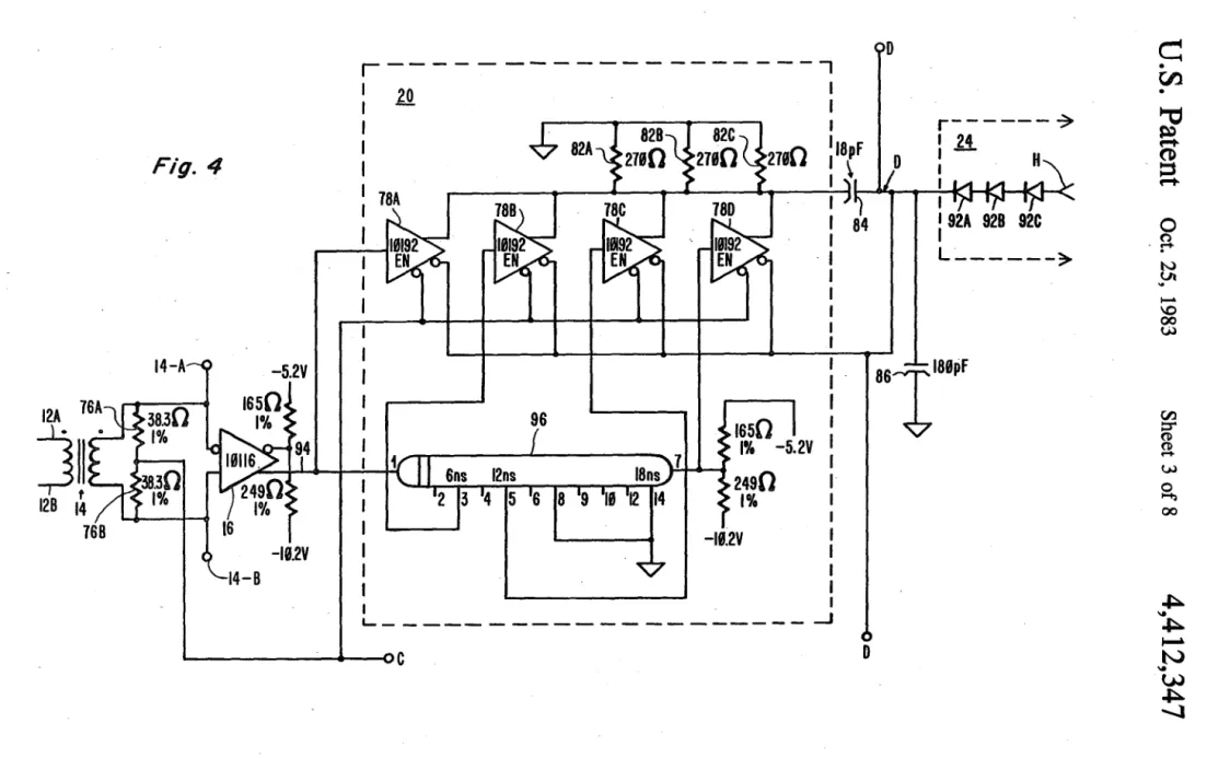
provided by a threshold setting network 64. In addition FIG. 4 shows the basic circuitry for the transmitter of to the threshold voltages supplied to the collision detec- the transceiver. The signal to be transmitted is applied tor and receiver squelch, the threshold setting network to the primary winding (i.e., leads 12A and 12B) of a 64 also provides
a
feedback signal (at point B) whose transformer 14. The secondary winding of transformer value is proportional to the threshold signal. This feed~ 30 14 provides the input of a buffer amplifier, or line re-back signal is sensed by a comparison amplifier 72 in the ceiver 16. A pair of matched resistors 76A and 76B are power supply 70 (shown in FIG. 3), to control one of also connected in series across the secondary winding of the two power supply outP1Ji. voltages. , , transformer 14, for impedance matching. A center tap is Power supply 70, in FIG. 3, employs a d.c.-to-d.c. provided at the junction of the two resistors 76A and converter 74 to generate Ii''''': 10.2 volt d.c. supply from 35 76B, and is labelled point C. Point C is connected to a a host power supply of +9.4 to + 15.75 volts. In addi- similarly labelled point on FIG. 6, at the output of the tion, a shunt regulator 76 provides a - 5.2 volt supply squelch circuit. The non-inverting output of buffer am-derived from the -10.2 volt source. The shunt regula- plifier 16, on line 94, provides the signal input to the tor 76 is controlled by a comparison amplifier 72 ~hich, cable driver 20.compares a voltage established by zener diode 78'with 40 Cable driver 20 is a current source 'which may be the feedback voltage generated at point B in the thresh- turned on and off to drive the coax cable channel with old setting network 64 of FIG. 2. Thus, the actual out- a binary waveform. The output from cable driver 20, put level of the nominally - 5.2 volt supply is adjusted ' however, is not simply a square wave type of output. It
and regulated so as to maintain the feedback voltage at has been found desirable to provide a staircase ramp point B equal to the voltage established by zener diode 45 rather than an abrupt leading and falling edge transition. 78. Consequently, the output of regulator 76 may be Thus, from a square wave input, the cable driver 20 greater or less than - 5.2 volts, as required to provide generates a well-controlled symmetric trapezoid wave-precision setting of the threshold by the threshold set- ,form, through a two-pole RC network which gives a 25
ting network 64. ' ns rise-time. This gets rid of much of the high frequency
The magnitude of the -10.2 volt supply is estab- 50 energy in the binary waveform without phase-distorting Iished by a feedback signal provided on line 75. That the zero crossings. If a square wave had been used, feedback'signal is an error voltage developed by ampli- rather than a staircase, larger filter capacitors' would fier 360. Amplifier 360 compares the output from d.c.- have been needed, thus causing unacceptable phase to-d.c. converter 74 with a reference voltage developed distortion.
7
4,412,347
8
inverted outputs of current switches 78A-78D are con-nected to the other lead of capacitor 84, which connec-tion also provides the cable driver output, at point (or node) D. There are four other connections to node D, as well: (1) a second filter capacitor 86, connected be- 5 tween node D and the transceiver ground; (2) a series string of three diodes 92A-92C connected between node D and the coaxial cable, comprising isolation cir-cuit 24; (3) guard switches 26, connected from node D
to ground; and (4) a transmit bias current switch, shown 10
in FIG. 6.
understood that the same explanation applies with re-spect to the other guard circuits.
Guard circuit 25A comprises a guard switch 26A and a guard switch timer 28A, which includes transistors 102A, 104A and 106A, plus their associated compo-nents. Guard switch transistor 26A is connected as a simple common emitter switch with its emitter attached to the transceiver ground and its collector attached to the node D of FIG. 4. When actuated, the switch tran-sistor 26A shorts out node D to ground. It is open only when there is a valid signal to transmit. A guard circuit The enable/disable terminals of the current switches driver comprising OR/NOR gate 108 and transistor 112 78A-78D receive an enable/disable signal at point C, controls the operation of guard switch timer 28A. from the transmitter squelch circuit of FIG. 6. A "stuck on" current switch 78A-78D will draw
In isolation circuit 24, three diodes are connected in 15 current from the guard switch(es) rather than the net-series to protect against the possibility of one, or even work.
two diodes short circuiting. Should point D be When the signal at connection point E from the trans-grounded, diodes 92A-92C become back-biased (open mitter squelch circuit of FIG. 6 changes state to indicate circuits) during other hosts' transmissions, thereby iso- the beginning of a transmission (Le., it goes high), tran-lating the transmitter from the network. Conversely, 20 sistor 112 emitter goes low and diode 116 becomes back the sole result of an open diode is to cause single station biased, allowing resistor 122 to discharge capacitor 118. failure, while leaving the network intact. The isolation Resistor 122 controls the rate at which capacitor 118 network provides important protection, because the discharges. When capacitor 118 is discharged suffi-transceiver is direct coupled to the network cable. ciently, the voltage across it turns off transistor 104A.
The operation of cable driver 20, when enabled, is as 25 Transistors 104A and 106A are an emitter-coupled pair, follows: A transition from zero to one on line 94, the so when transistor 104A turns off, transistor 106A turns asserted output of buffer 16, turns on current switch on, activating switch 26A and driving transistor 26A 78A (the first stage of the ramp generator) and also is into saturation. Thus, a predetermin.,d time after the supplied to the input of a delay line 96 and begins to beginning of a "stuck" transmission, all of the guard propagate therethrough. Delay line 96 is tapped three 30 switches are turned on, shorting the output of cable times at, for example, 6 nanoseconds, 12 nanoseconds driver 20 and effectively disconnecting it from the ca-and 18 nanoseconds of delay. The 6 nanosecond delay ble. At the end of an "unstuck" transmission, transistor provides the input to the second stage current switch 112's emitter goes high, turning switch 26A on, also 78B, to turn it on 6 nanoseconds after current switch recharging capacitor 118 via diode 116 in preparation 78A was turned on. Similarly, the 12 nanosecond tap is 35 for a subsequent transmission.
connected to the input of third stage 78C and the 18 Turning now to FIG. 6, there is shown the remainder nanosecond output drives the fourth stage 78D. Be- of the transmitter circuitry, including squelch and other cause the current switches 78A-78D are connected in control circuits.
parallel and draw current through the same load, they Amplifiers 152 and 154 plus the associated compon-provide additive outputs, with the amplitude of the 40 entry form the transmit squelch circuit. This is a con-output signal increasing each time another one of those ventional type of squelch circuit whose operation will switches is turned on in their machine-gun firing se- be readily understood from the drawing by those skilled quence, thereby providing the staircase signal. Resistors in the art. Accordingly, a detailed explanation is unnec-82A-82C and capacitors 84 and 86 provide a two-pole essary to the understanding of this invention. The RC filter for smoothing the output signal. 45 squelch circuit monitors the transmit signal from the Referring now to FIG. 5, guard circuits 25A-25C for host (which appears across points 14-A and 14-B, the shorting the output of the cable driver 20 are shown. secondary leads of transformer 14) and provides two The guard circuits comprise a plurality of switches outputs, the cable driver enable/disable signal which is 26A-26C connected in parallel, each having one term i- provided on line 156 (point C) and the complement to nal connecting to the transceiver ground and the other 50 that signal which is provided on line 158.
terminal connected to node D. The switches are all Transistors 162 and 164 comprise an emitter-coupled controlled by a common driver 32 (gate 108 and transis- pair. The base of transistor 162 is driven by the non~
tor 112); and the driver is operated bya signal supplied asserted output of amplifier 154, on line 156. The collec-at point E, which indiccollec-ates the start of each transmis- tor of transistor 162 supplies an output signal at
connec-sion. . 55 tion point E, which connects to a similarly labelled
9
4,412,347
due to the effect of differentiation produced bycapaci-tor 174. This turns on transistor 182 for a like duration and produces a collision test signal at the collector of transistor 182, which is shown as a point F to be con-nected to a similarly marked point on FIG. 7, in the 5 low-pass filter of the.receiver.
The collision test signal simulates the effect of a colli-sion by drawing excess current through the receiver input at the end of every packet transmitted. Transistor
204 isolates the collision test signal from the network, so \0
it is not seen by other stations; only the transmitting station responds to it. Further, this collision test does not suffer from "single point of failure" problem. The host, of course, must check at the end of each transmis-sion for the presence of the "collitransmis-sion signal" generated 15 by the collision test signal.
Attention is now directed to the aforesaid FIG. 7, which illustrates the low-pass filter, receiver squelch, collision detector, collision oscillator and threshold setting circuits. Connection point H is the receiver input 20 from the coaxial cable (and, of course, the transmitter output, as well). It is attached to a fusible resistor 202
which provides protection against a short circuit in transistor 204 having any adverse impact on the net-work. Transistor 204 is connected as a unity gain emit- 25 ter-follower. A current source comprised of transistor
206 and resistor 208 biases transistor 204 so that it is always conducting.
Transistor 214 and the associated components (capac-itors 216, 218 and 222 plus resistors 224, 226 and 228) 30 provide an emitter-follower circuit configured as a three-pole low-pass filter. The output of the low pass filter, on line 232, represents the average value of the signal on the cable, offset by the base-emitter voltage drops of transistors 204 and 214. The signal on line 232 35 is compared against two· thresholds. One threshold is used to determine whether there is a single signal on the cable (in which event the receiver squelch should be turned oft) and another threshold is used to determine whether there are two or more signals on the cable (in 40 which event a collision is indicated). These thresholds are applied, respectively, to the inverting input 234 of a differential line receiver which is used as a comparator
236 and to the inverting input 238 of a similar compara-tor 242. The signal on line 232 is supplied to the non- 45 inverting input 244 of comparator 236 and, through a resistor 246 to the non-inverting input 248 of compara-tor 242.
The two thresholds are set by a precision current source comprising transistor 252 plus a compensation 50 circuit comprising transistors 258 and 262. The base of transistor 252 is connected to the - 5.2 volt supply and its emitter is connected to the -10.2 volt supply through a resistor 264. Resistor 264 is a high precision resistor; the voltage across it sets the emitter current of 55 transistor 252. The power supply adjusts the precise value of the regulated output (which is nominally -5.2 volts) to achieve the desired current through resistor
264. To this end, the voltage at the emitter of transistor
252 is sensed by the power.supply and a connection to 60 the power supply is shown at a point labelled B. Tran-sistor 258 is connected as a similar current source with an emitter resistor 266 having the same value. as resistor
264, to produce the same emitter current.
Transistor 262 is the load for current source 258 and 65 its sole purpose is to draw a base current into transistor
262 which will raise-the current drawn through resis-tors 268 and 272 by an amount which very nearly equals
10
the difference between the collector current and emitter current of transistor 252. Thus, transistor 262 is in-tended to compensate for the fact that transistor 252 has a finite current gain as a result of which its collector current does not exactly equal its emitter current, by pulling a current through resistors 268 and 272 which is very close to the emitter current through resistor 264.
Preferably, transistor 252 and 262 will be provided on the same subst~ate so as to provide matching current gain, and thereby set the current in resistors 268 and 272
exactly equal to the emitter current of transistor 252.
The actual threshold voltages are developed across resistors 268 and 272 plus the sum of the base-emitter drops a~ross transistors 254 and 256. Transistors 254
and 256 are used to match the corresponding base-emit-ter drops of transistors 214 and 204.
Preferably, transistors 256 and 204 will be provided on the same substrate so that their base-emitter voltage drops will match and transistors 254 and 214 will also be provided on the same substrate, for the same reason.
The signal provided on line 232, to be compared with the reference thresholds, is produced by filtering the sum of the signal received over the coaxial cable and the collision simulation test signal supplied at point F.
The comparator 236 drives a buffer amplifier 274, the output of which provides the receiver squelch signal at point K, which is connected to the similarly labelled point in FIG. 8.
The comparator 242 detects whether the collision threshold has been exceeded. In turn, it drives a buffer amplifier 276 which turns on and off a 10 MHz oscilla-tor formed by OR/NOR gate 278, capacitors 282 nd
284, inductor 286 and resistor 288. The OR/NOR gate
278 provides a balanced output for driving a trans-former 292 through which a collision presence signal is supplied to the host device.
Turning now to FIG. 8, the receiver circuitry will be explained in detail. The receiver gets its input at point L, the emitter of transistor 204 in FIG. 7. Resistor 302
and capacitor 304 filter out the high frequency compo-nents in the received signal. Transistor 306 is an emitter follower which acts as a buffer and provides a low impedance output to drive a high pass filter comprising capacitor 308 and resistor 312, on the non-inverting input of a differential line receiver amplifier 314.
The output of amplifier 314 feeds another buffer am-plifier stage 316. The receiver squelch signal from am-plifier 274 (connection point K) is also connected to the output of buffer amplifier 316. Since this is emitter-cou-pled logic, if the output of either amplifier 274 or ampli-fier 316 is high, then their common connection (point K) is high. Thus, the output of amplifier 316 is squelched, or turned off, by maintaining the output of amplifier 274 high.
The output of amplifier 316 also feeds the non-invert-ing input of another amplifier stage 318, which then feeds an OR/NOR gate 320. Gate 320 provides gain and also presents a balanced differential output signal to drive a transformer 322 through which the receive signal is communicated to the host device.
11
4,412,347
is well-developed in the electrical arts. Thus, forpur-poses of this explanation, it is sufficient to note that the d.c.-to-d.c. converter 74 receives a positive voltage at terrriinal Mrelative to an input power return, or ground, at terminal N and that it supplies an output voltage at a '5 terminal P relative to an isolated transceiver ground at terminal R. A co-operating voltage regulator shown in FIG. 10, is connected to terminals P and R. This volt-age regulator also supplies a feedback signal to a point S in the converter, responsive to which the d.c.-to-d.c. 10 converter adjusts its output voltage.
Turning now to FIG. 10, the regulator circuitry is shown for taking the voltage supplied at terminal P, regulating it at - 10.2 volts and providing a further regulated output of - 5.2 volts at point.
A 4.3 volt zener diode 78 is connected across the 10.2
volt supply through a series 590 ohm resistor 358, to provide a precise reference point 4.3 volts above (i.e., more positive than) the nominally - 10.2 volt supply, at
15
the non-inverting input 359 of operational amplifier 360. 20 A precision resistive divider network 362 and 364 is designed to provide 4.3 volts at the inverting input 366
of amplifier 360 when the voltage across terminal points Rand P is precisely 10.2 volts. The output of amplifier
360 provides a feedback signal to the d.c.-to-d.c. con- 25 verter 74, at point S. The feedback signal supplied to point S represents the error between the 4.3 volt refer-ence provided by zener diode 78 and the voltage mea-sured at the inverting input of amplifier 360, and, thus, the amount by which the voltage at terminals P, R 30 differs from 10.2 volts. The d.c.-to-d.c. converter 74
responds to the feedback signal at point S by adjusting its output so as to eliminate any error signal.
The 4.3 volt signal across zener diode 78 is also'ap-plied to the non-inverting input of comparison amplifier 35
72, as a reference for the - 5.2 volt supply. Unlike the
-10.2 volt supply, however, the output of the -5.2
volt supply is not forced to bear a definite relationship to the zener diode voltage. Rather, a particular point in the threshold circuit (powered from the - 5.2 volt sup- 40 ply) is forced to have a definite relationship to that voltage. The inverting input of amplifier 72 receives the signal generated at point B of FIG. 7, the current source for the threshold-setting network. The output of ampli-fier 72 controls a shunt regulator comprised of transis- 45 tors 372 and 374, as well as capacitors 376, 378, 382 and
384, to provide a regulated - 5.2 volt output at point T. The resulting precise regulation is at point B, where it has direct effect on the precision of threshold-setting.
Amplifier 72 senses a point remote to the power sup- 50 ply itself, where a specific voltage (equal to the zener diode voltage) should appear; it compares the sensed voltage with the reference voltage established by the zener: diode and drives the shunt regulator output to force 'the remote, monitored voltage to equal the refer- 55 ence voltage. Any deviation between the two produces an error signal which causes either transistor 372 or 374
to be driven harder, thus shifting the electrical position
12
tions and improvements 'as are obvious herefrom be included within the scope of this invention. The inven-tion is intended to be limited only as defined in the appended claims, the foregoing description being illus-trative only, and not limiting. '
Having illustrated and described my invention, I
claim: '
1. A precision combination voltage and current source comprising:
means for providing a first d.c. power supply voltage; regulator means for providing a second d.c. power supply voltage derived from said first voltage, the amplitude of the second voltage being variable responsive to a control signal;
a current source energized by and having an output that varies with the second voltage;
a means within the current source for developing a voltage across a resistor proportional to the output of the current source;
means for providing a precision reference voltage equal to the desired voltage across said resistor; and
means for comparing the voltage across the resistor with the precision reference voltage, and for gener-ating the regulator control signal in response to the comparison,
whereby the second d.c. power supply voltage is driven by the control signal to a value which causes the voltage across the resistor to tend to equal the reference voltage, thereby simulta-neously providing the voltage needed to establish the output of the current source at the desired level and also providing the desired second power sup-ply voltage.
2. The apparatus of claim 1 wherein the means for providing the first power supply voltage further in-cludes means for comparing the first power supply voltage with the reference voltage and means for main-taining the first power supply voltage in a predeter-mined relationship with the reference voltage,
whereby the first d.c. power supply voltage ,and the output of the current source simultaneously are constrained to their intended values by comparison with a single reference voltage, and the regulator means provides the voltage' needed to drive the current source to its desired output level while simultaneously providing the second power supply voltage for other uses.
3. In a transceiver for a carrier-sense multiple access communications network with collision detection, such network including a communication channel such 'as a coaxial cable chain wherein the precise setting of first and second threshold voltages is required for use'in collision detection, the first threshold being set at a level to distinguish between the absence or presence of sig-nals on the cable and the second threshold being set at a level to distinguish between the presence of two or more signals on the cable or fewer number of signals on of their emitter connections relative to the 10.2 volt
supply.
This circuit thus permits a single z'ener didde refer-ence to be used to regulate two different supply volt-ages, one in the power supply and the other in one of the circuits powered by the supply.
60 the cable, the presence of two or more signals constitut-ing a collision, a circuit for the precision settconstitut-ing of volt-ages and currents to 'establish such threshold voltvolt-ages, comprising: '
Having thus described the invention, it will be appar- 65 ' ent that various modifications, alterations, and improve-ments will readily occur to those skilled in the art. Ac-cordingly, it is intended that such alterations,
4,412,347
13
a current source energized by and having an otltput that varies with the second voltage;
means within the current source for developing a voltage across a precision resistor the voltage being proportional to the output of the current source; 5 means for providing a precision reference voltage
equal to the desired voltage across said resist'or; means for comparing the voltage across the resistor
with the precision reference voltage, and for gener-ating the regulator control signal in response to the 10 comparison;
the means for providing the first power supply volt-age including means for comparing the first power supply voltage with the reference voltage and means for maintaining the first power supply volt- 15 age in a predetermined relationship with the refer-ence voltage; and
first and second precision resistors connected in series to the output of the current source such that the
20
25
30
35
40
45
50
55
60
65
14
output current of the current source passes through those resistors, the values of those resistors being selected to develop across them first and second voltages, respectively, to provide the first and sec-ond thresholds,
4. The apparatus of claim 3 wherein the network includes a communications channel and further includ-ing:
means responsive to signals on the channel for pro-viding an average value signal corresponding to the average vlllue of the signal on the cable; and comparison mellnsfor comparing the average value
signal with the first and second thresholds, the comparison means signalling the absence of a signal on the cable, when the average value signal is less than the first threshold and signalling the detection of a collision. when the average value signal ex-ceeds the second threshold.