PROGRAMMERS' REFERENCE MANUAL
Honey","ell
ELECTRONIC DATA PROCESSINGPRICE . .
.
..
.
..
.
$3.00
Questions ond comments regording this monuol should be oddressed to:
Honeywell Electronic Data Processing Information Services
60 Walnut Street
HONEYWELL
FIRST EDITION First Printing, August, 1964
Copyright 1964 Honeywell Inc.
Electronic Data Processing Division
This manual is intended as a detailed reference source for programming the Honeywell
.
300 Electronic Data Processing System. It contains a functional description of the system
components and a detailed explanation of the instruction repertoire. No previous knowledge
Section I
Section II
Section III
Section IV
Section V
Section VI
T ABLE OF CONTENTS
Page
The Central Processor . . . . Control Panel . . . . Main Memory . . . .
Control Memory. . . . 1
Control Unit. . . • . . . 3
Arithmetic Unit. . . 3
Memory Interlace. . . . 3
The Input/Output Systems . . . . 5
Exte rnal Line s. . . 5
Direct Input/Output Channel. . . . 5
Standard Peripheral Control. . . . 5
Priority Interrupt. . . . 7
Buffered Input/Output. . . • . . . 8
Information Format. . . . .. 11
Fixed-Point Word . . . '. 11
Floating-Point Word. . . .. 11
Alphanumeric Word. . . . .. 11
The Instruction Word. . . .. 12
The Indirect Address Word . . . 12
Addressing. . . . .. 15
Direct Addressing. . . .. 15
Indexed Addressing. . . . .. 15
Indirect Addressing. . . . .. 16
Indirect Indexed Addressing . . . 16
Expanded Memory Addressing . . . 16
Standard Instructions. . . . .. 19
General Specifications. . . . .. 19
Execution Timing. . . . .. 19
Indicators . . . 19
No-Address Instructions (NAD) . . . .. 19
Registers. . . .. 20
Symbology. . . . .. 20
Control Instructions. . . .. 20
Fixed- Point Instructions. . . . .. 24
Indexing Instructions. . . .. 25
Clas s I Indexing Instructions. . . . .. 26
Clas s II Indexing Instructions . . . . '.' . . . • . . . .. 27
Input/Output Instructions, D i r e c t . . . 28
Interrupt Instructions. . . . .. 29
Logic Instructions. . . . .. 31
Shift Instruction. . . . .. . . . .. 33
Word Transmission Instructions. . . . .. 33
Section VI (cont)
Section VII
Se ction VIII
Appendix A
Appendix B
Appendix C
Appendix D
Appendix E
Appendix F
Appendix G
Page
Multiply / Divide Instructions. . . . .. 41
Floating-Point Instructions. . . . . . . . . . . . . . . . . . . .. . .. . .. .. . .. . .. 41
Input/Output Instructions, B u f f e r e d . . . 43
Buffered Input/Output Operations. . . .. 49
Card Read Operations, Model 223. . . .. 49
Card Punching Operations, Model 224 . . . .. 52
Magnetic Tape Operations, Series 204B. . . .. 54
Print Operations, Series 222 . . . . . . . . .. . .. . . . .. .. . . . . .. . . . 61
Models 222-1, 222-2, and 222-3 . . . 61
Model 222-4 . . . " 62 Peripheral Devices. . . . . . . . . . . . . .. .. . . .. . . .. . . . .. . . . ... .. 65
Direct Input/Output Devices. . . . .. . . . .. . . . .. . . . .. . .. 65
Paper Tape Reader, Model 309 . . .. . . .. . . .. . . . . .. .. . . . ... .. 65
Paper Tape Punch, Model 310 . . . " 65 Keyboard Printer, Model 320. .. . .. . . . .. .. .. . . ... .. 65
Buffe red Input/ Output Device s . . . .. 65
Magnetic Tape Unit, Series 204 . . . " 66 Paper Tape Reader and Control, Model 209 . . . .. 68
Paper Tape Punch and Control, Model 210 . . . .. 69
Printe r s and Controls, Se rie s 222. . . .. 71
Models 222-1, -2, -3 . . . 71
Model 222-4 . . . . " . . . .. . . . .. . .. 72
Card Reader, Model 223 . . . . .. . . . . . .. . . . .. . . . .. . . . .. . .. . .. 73
Card Punche s, Se rie s 224. . . .. 74
Card Reader- Card Punch, Model 227 . . . .. 75
MICR Sorter-Reader Control, Models 233-1, - 2 . . . 76
Random Access Disc Storage and Control, Series 260 . . . .. 77
Random Access Drum Storage and Control, Series 270 . . . .. . .. 78
Single-Channel Communication Controls, Series 281 . . . . . .. . .. 78
Multiple - Channel Communication Control, Se rie s 284 . . . .. 79
Communication Control Adapter, Series 285 . . . , . . . .. . .. 80
Family Interface Units. . . .. 81
Magnetic Tape Switching Units, Series 205. . . . .. 81
On-Line Adapter, Model 2 1 2 - 1 . . . 82
Communication Switching Units, Series 215 . . . 83
Peripheral Control Switching Units, Series 216. . . . .. . . .. . . .. . .. 83
Twos-Complement Arithmetic. . . .. . . . . .. . . . . . . . . . .. . . . .. . . . . .. 85
H- 300 Character Code s. . . .. 89
Types of Machine Words. . . .. . .. . .. .. . . . .. . .. . .. . . . .. . . . . .. 91
Octal-Decimal Integer Conversion Tables. . . . .. . . . . . . . . .. 93
Octal- Decimal Fraction Conver sion Table s . . . " 99 Table of Powers of Two . . . " . . . 103
[image:7.616.104.554.125.708.2]Figure 1. Figure 2. Figure 3. Figure 4. Figure 5. Figure 6. Figure 7. Figure 8. Figure 9. Figure A-I.
Table I. Table II. Table III. Table IV. Table V. Table VI. Table VII. Table VIII. Table IX. Table X. Table XI. Table XII. Table XIII. Table XIV. Table XV. Table XVI. Table XVII. Table XVIII. Table XIX. Table XX. Table XXI. Table XXII. Table XXIII.
LIST OF ILLUSTRATIONS
Page
The Direct Input/ Output Channel. . . . .. 6
Buffered Input/Output Data Path. . . . .. 8
Types of Main Memory Addressing . . . 15
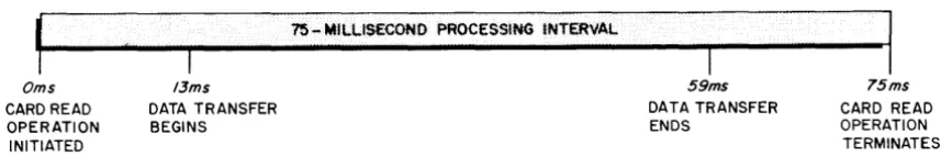
Model 223 Card Read Operation . . . 49
Print Operation for Models 222-1, 222-2, and 222- 3 . . . 61
Print Operation for Model 222-4 . . . 62
Multiple Communication Control, Series 284 . . . 80
Magnetic Tape Switching Units, Series 205 . . . 82
Communication Switching Unit, Models 215-1, -2 . . . 83
Twos - Complement Arithmetic . . . 87
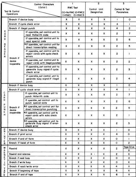
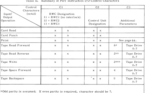
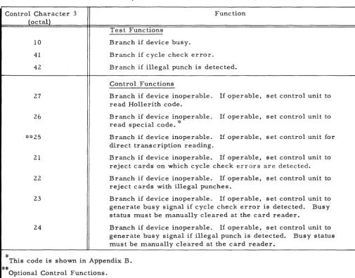
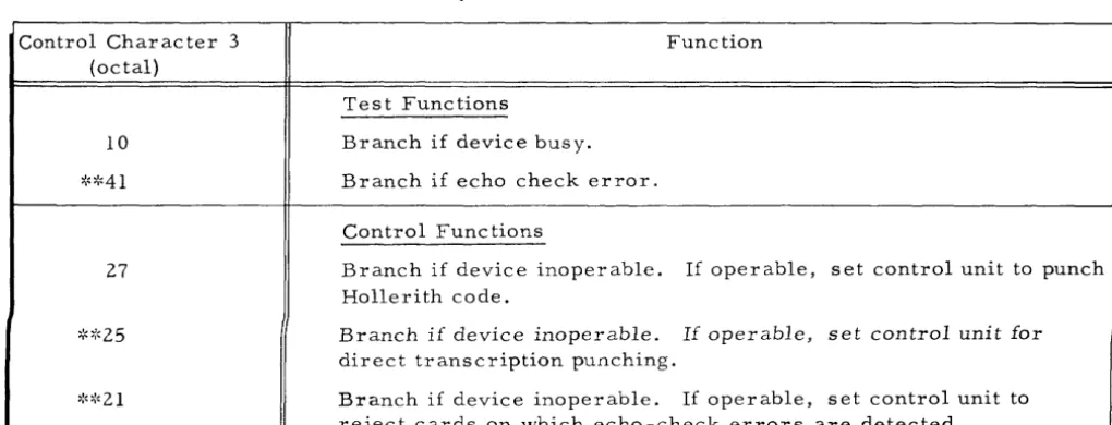
LIST OF TABLES Summary of PCB Instruction I/O Control Characters . . . 46
Summary of PDT Instruction I/O Control Characters . . . 48
Summary of Card Reader PCB Functions (Model 223) . . . 51
Model 224 Card Punching Speeds . . . 53
Summary of Card Punch Control Parameters . . . 53
Tape Unit Characteristics . . . 55
Tape Unit Simultaneity and Busy Conditions . . . 58
Summary of Magnetic Tape PCB Functions (Serie s 204B) . . . . • . . . 59
Summary of Magnetic Tape PDT Functions (Serie s 204B) . . . • 60
Summary of Printer PCB Functions (Series 222) . . . 63
Summary of Printer PDT Functions (Series 222) . . . 64
1/2-Inch Magnetic Tape Units, Series 204B . . . 67
3/4-Inch Magnetic Tape Units, Series 204A . . . 67
Paper Tape Reader and Control, Model 209 . . . 69
Paper Tape Punch and Control, Model 210 . . . 70
Printers, Series 222 . . . 72
Card Reader, Model 223 . . . .' . . . 74
Card Punch, Models 224- 1, - 2 . . . 75
Card Reader-Card Punch, Model 227 . . . 76
Random Access Disc Units, Series 260 . . . 77
Random Access Drums, Series 270 . . . 78
Single-Channel Communication Control, Series 281 . . . 79
The Model 301 central processor is the computing and control center of the Honeywell 300
system. Functionally, it is composed of high-speed magnetic core main memory and control
memory, an arithmetic unit, a control unit, and a direct input/ output channel.
A major design feature of the central processor is the use of integrated system modules.
Each module contains all of the circuitry required for a specific function. For example, one
module contains all of the card control circuitry, another contains the arithmetic unit, and so
on. This modularity greatly enhances the expandibility of the system. In most cases, expansion
involves little more than plugging in additional modules. The reliability of the modular
com-ponents has been enhanced through the use of high-temperature lithium ferrite cores and silicon
semic onductor s.
CONTROL PANEL
An operator's control panel is included in the basic system. This panel contains displays
for the important arithmetic and control unit registers together with six sense switches for
manually controlling the path of the program. Controls are also provided for starting and
stopping a program and for interrogating main memory and control memory.
MAIN MEMORY
The main memory contains 4,096 locations, each capable of storing one 24- bit word and
one automatically generated and checked parity bit. Additional memory is available in modules
of 4, 096 words up to a system total of 32,768 words. Thereafter, additional memory is available
in modules of 8,192 words up to a system total of 65,536 words.
One memory cycle (that is, the time required to retrieve a word from a memory location
and restore the cores to their original states) is 1. 75 microseconds. The memory has an
operating range of 00 to 1250 Fahrenheit. The contents of memory are protected when power is turned on or off.
CONTROL MEMORY
The control memory contains sixteen 24-bit words of storage, comprising six index
regis-ters, eight general-purpose regisregis-ters, the accumulator (A register), and the auxiliary arithmetic
register (B register). It is driven as a linear-select memory with a split 500-nanosecond cycle
(250-nanosecond read and 250-nanosecond write). The contents of control memory are protected
SECTION 1. THE CENTRAL PROCESSOR
SUITunary of H-300 Central Processor Characteristics
INFORMATION UNIT
MEMORY CAPACITY
CONTROL MEMORY
ACCESS TIME
CYCLE TIME
PROCESSOR SPEED
INTERNAL OPERATIONS
INSTRUCTION FORMAT
ADDRESSING
CHECKING
HARDWARE BYPASS
DIREC T INPUT/OUTPUT CHANNEL
EXTERNAL LINES
READ/ WRITE CHANNELS
SENSE SWITCHES
INDEX REGISTERS
PRIORITY INTERRUPT
TEMPERATURE RANGE
POWER FAILURE PROTECTION
24- bit word.
4,096 words (16,384 characters), expandable to 65,536 words {262, 144 characters}.
16 words.
Main memory: 875 nanoseconds. Control memory: 250 nano-seconds.
Main memory: 1. 75 microseconds. Control memory: 500 nano-sec onds.
Fixed-point add to accumulator: 3.5 microseconds. 285, 000 fixed-point binary add instructions per sec ond without memory interlace; up to 380, 000 with interlace. Gibson mix: 180, 000 instructions per second without interlace; 236, 000 with interlace.
Fixed-point, twos -c omplement binary arithmetic; logic; c ontr 01; and input/ output. Optional multiply, divide, floating-point, and character instructions.
Single-address, variable format. A typical instruction includes an op code, a variant character, and an address field.
Direct main memory within a 32, 768-word bank, indexed main memory, indirect main memory, and indirect indexed main memory. Optional facility to address individual characters.
One parity bit automatically generated and checked in each main memory word.
Use of an optional instruction which is not installed in the machine causes a subsequence to a fixed memory location. The program may there identify the instruction and execute it by means of a subroutine.
One 24- bit, non- buffered input bus and one 24- bit non- buffered output bus, with control lines and an interrupt line. Up to 64 peripheral devices may be directly addressed by this channel. A standard peripheral control is supplied which services the keyboard printer, the paper tape reader, and the paper tape punch.
15 external sensing lines and 15 external activating lines.
Up to three optional read/ write channels. Data transfer over these channels can occur simultaneously with computing.
Six.
Six.
Six levels, expandable to 24 levels.
The temperature range of the central processor (including memory) is 00 to 1250 Fahrenheit.
CONTROL UNIT
The control unit controls the flow of information within the central processor; it selects,
interprets, and controls the exec ution of all instructions and governs addre s s selection within
the main memory. The control unit includes a sequence register, an operation code register,
a shift counter, a clocking system, and subcommand generators.
ARITHMETIC UNIT
The arithmetic unit pe rf orms twos - complement arithmetic oper ations, as well as logical,
shift, and comparison operations. The arithmetic registers that are accessible by program
are located in the control memory. The arithmetic unit also includes an addend register, an
augend register, and some auxiliary circuitry; these are not accessible by program.
MEMORY INTERLACE
In systems containing more than 8, 192 words of memory, an interlace option is available
which permits simultaneous addressing of two or more 8, 192-word blocks. Using this option,
if the program is stored in one block and data are stored in another, the central processor
can automatically overlap operand processing for the current instruction with retrieval of the
next instruction. Execution times for instructions may thereby be reduced by as much as one
memory cycle.
In systems containing both the buffered input/ output (i. e., one or more read/ write
channels) and the memory interlace features, if data transfer uses a memory block not used
in computing, the transfer is overlapped with computing. That is, data may be transferred
into or out of one block while the program is proces sing instructions in another block. To
achieve both the instruction interlace and the input/ output interlace, more than two blocks of
memory are required. Then operand processing, instruction retrieval, and input/output can
SECTION II
THE INPUT/ OUTPUT SYSTEMS
The standard input/ output systems consist of two sets of external lines, a direct input/
output channel, a standard peripheral control, and a priority interrupt system.
EXTERNAL LINES
There is a set of 15 activating lines from the central processor to external points and
another set of 15 sensing lines from external points to the central processor. Two instructions
address these lines. The STE (Set External Point) instruction delivers a pulse to the external
activating line( s} specified by the low- order 15 bits of the instruction. The SKE {Skip if Signal
Not Set} instruction examines the external sensing line{s} specified by the low-order 15 bits of
the instruction. If any of the external sensing lines tested is not set, the next instruction is
skipped. Any combination of external lines may be set or tested with the appropriate instruction.
DIRECT INPUT/OUTPUT CHANNEL
The H-300 is equipped with a direct input/ output channel consisting of a 24-bit input bus,
a 24-bit output bus, an interrupt line, and a set of control lines {see Figure l}. The control
lines carry control pulses, data pulses, and responses from peripheral control units. Control
pulses and data pulses are used to define the meaning of the information that is on the input or
output bus. The addressed peripheral control interprets the pulses and control information
and either issues a response or directs the actions of the attached peripheral devices.
Standard Peripheral Control
A standard peripheral control which services a keyboard printer, a paper tape reader,
and a paper tape punch is part of the central processor. The control is permanently attached
to the direct input/ output channel as illustrated in Figure 1. Up to seven additional peripheral
controls handling up to 60 additional devices may be attached to the direct input/ output channel.
Since the devices controlled by this unit read or write one character at a time, the control is
designed to receive or transmit the largest of the characters, which is the eight-bit character
fr om the eight- channel paper tape devic e. The devic e s that may be connected to the standard
control are as follows:
CONTROL
C
-E LINES
N T R A
L INTERRUPT ... LINE P
R
0
C
E INPUT
S BUS
S 0 R OUTPUT BUS .~
1r
.
~ ATO ADDITIONAL PERIPHERAL CONTROLS
,
STANDARD PERIPHERAL CONTROL
[image:13.613.47.555.68.434.2]..
Figure 1. The Direct Input/ Output Channel
~
-
READER...
-..
~
PUNCH -PRINTER..
(KEYBOARD)-~
..
~
Three instructions are used in conjunction with the direct input/ output channel. These
are the Control and Skip instruction (SKC), the Peripheral Input instruction (PIN), and the
Peripheral Output instruction (POT). The SKC instruction generates control pulses to inform
the peripheral controls attached to the direct input/ output channel that the bus contains control
information. The PIN and POT instructions transfer data to and from the central processor,
respectively.
Operation of the Standard Peripheral Contr 01
When anyone of the devices attached to the standard peripheral control is ready to transmit
or receive information, an interrupt signal is generated on the interrupt line servicing the direct
input/ output channel. The pr ogr am may then sc an the devic esc onnec ted to the standard c ontr 01
to determine which one caused the interrupt. This is done by means of a series of SKC
in-structions which interrogate each attached device in turn. When the device issuing the interrupt
SECTION II. THE INPUT/OUTPUT SYSTEMS
When an SKC instruction is executed, the specified control line is energized. All the
peripheral controls attached to the bus examine the bits on the control line. These bits
desig-nate the address of the device to which the SKC instruction is directed as well as the question
or command to be interpreted by the peripheral control.
Only the addressed device responds to the SKC instruction by connecting itself logically
to the bus. If a response is requested by the SKC instruction, it is sent over the appropriate
response line to the central processor; if a response is not received within a set time period
(e. g. , if a non-existent device is addressed or if the addressed device has been powered down),
a negative response is assumed.
When a PIN or POT instruction is issued, a "ready" response is required. Since only
one device may be connected logically to the bus at a time, there can be no ambiguity as to which
devic e is to respond. If the re sponse is positive, the instruc tion is exec uted and the next
in-struction is skipped. If the response is negative, the instruction is not executed but the next
instruction is executed. In any case, the central processor does not stall while waiting for a
peripheral device.
Priority Interrupt
The H-300 has six levels of priority interrupt. These may be optionally expanded in groups
of six levels to a maximum of 24 levels. One of the basic six interrupt lines is associated with
the dir ect input/ output channel.
The priority interrupt system features automatic generation of subsequence addresses
for each external line according to a fixed priority, with the ability to block (disable) individual
lines selectively. Priority of the interrupt lines is determined according to bit position in the
interrupt register, with the high- order bit position having the highe st priority.
Blocking
Only the bit positions in the interrupt register for which there is a corre sponding one- bit
in the interrupt mask register can cause a subsequence. The mask register may be loaded from
memory by using the LIM (Load Interrupt Mask) instruction or its contents may be exchanged
with memory using the XML (Exchange Interrupt Mask) instruction.
The interrupt block is automatically set when a subsequence occurs. It remains set until
Operation of the Interrupt System
If (1) an interrupt signal exists when execution of an instruction has been completed, (2)
one or more bits of the interrupt register contain a one, (3) the corresponding bit(s) in the
interrupt mask register are one, and (4) the interrupt block is not set, a subsequence is
auto-matically made to the address corresponding to the bit of highest priority and the interrupt block
is set. The bit corresponding to the interrupt line which caused the subsequence is cleared to
zero in the interrupt register. All other interrupts which are present when the block is set or
which are generated after the block is set are remembered for later servicing when the interrupt
block is cleared. Clearing of the interrupt block by means of the Set/ Reset Interrupt Block
instruction (SRB) is delayed long enough to permit one additional instruction to be executed before
the block is cleared. Thus, uninterrupted execution of the instruction following the SRB
in-struction is guaranteed.
BUFFERED INPUT/OUTPUT
Up to three optional read/write channels may be installed which permit simultaneous
operation of up to three peripheral devices with either a direct input/ output operation or
comput-ing. Buffered input/ output makes it pos sible, for example, to print, read and write tape, and
compute - all at the same time.
Simultaneity of operation is achieved through time sharing and is based on the fact that
all input/output operations require access to the main memory for only a small part of the time
that they are in progress. Therefore, when an input/ output operation is in progress but is not
using the main memory, another peripheral device or the central processor may gain access
to the main memory. It is the function of the input/ output traffic control to direct the time
sharing of the main memory by the various peripheral devices and the central processor.
In order to understand how the traffic control does this, the programmer must have an
understanding of how data is transferred between a peripheral device and the main memory.
Figure 2 illustrates the basic elements which form the data path between a peripheral device
and the main memory.
$ ~ ~Hi!' $
'~.'~ ~.~
~
I-MAIN MEMORY
TRAFFIC CONTROL
PERIPHERAL
INTERFACE
---.,
-
-
INPUT/ OUTPUT TRUNK.
PERIPHERAL ---CONTROLFigure 2. Buffered Input/ Output Data Path
PERIPHERAL
[image:15.610.102.499.601.706.2]SECTION II. THE INPUT/OUTPUT SYSTEMS
Input/ Output Trunks
The H-300 System can be equipped with eight input/ output lines (expandable to 16) which
permanently connect the control units of the various peripheral devices to the peripheral
inter-face. For example, a card reader and its control are permanently connected to the interface
via an input trunk, while a printer and its associated control are attached via an output trunk.
Each of these trunks is 6 bits wide and is therefore compatible with all standard Honeywell
peripheral controls.
Read/ Write Channels
Notice that the data path shown in Figure 2 is incomplete: there is no connection across
the peripheral interface. This final link in the data path, known as a "read/ write channel, " is
inserted when an input/ output instruction is executed. Up to three read/ write channels, labeled
RWC1, RWC2, and RWC3 are available as options.
When the programmer codes an input/ output instruction, he specifies, among other things,
the peripheral control that is to receive or transmit data and the read/ write channel over which
the data transfer is to take place. For example, an instruction might specify a card read
opera-tion in which the card reader control transmits data over RWC2. When this instruction is
executed in the stored program, the data path will look like this.
MAIN
TRAFFIC
MEMORY
-
CONTROL ( RWC2>
1 4 -1/<-:-"'0-.... TRUNKCARD READER CONTROL
CARD READER
As soon as the data transfer is completed, RWC2 is automatically removed from the interface.
This means that the pr ogrammer can as sign R WC2 to another peripheral contr 01 in another
input/ output instruction. This is an extremely important feature. There is no predefined
relationship between the read/write channels and the peripheral devices. The programmer
can assign read/write channels with complete freedom.
Each read/write channel consists of a current location counter, a starting location counter,
two buffer registers, a current word counter, a starting word counter, and a character counter.
instruc-When a six-bit (character) trunk is being controlled, there is provision for automatic
packing or unpacking of the characters to or from 24-bit words. The character counter is
incremented by one as each successive character is transferred. Each time the character
count passes four, the contents of the present location counter and the word counter are also
incremented by one.
Traffic Contr 01
While a peripheral operation is in progress, it requires access to the main memory for
only a fraction of the total time to complete the operation; most of the time is taken up by
mechanical activities. Therefore, there is time available for another peripheral control to
transfer data to or from the memory via another RWC. This second input/ output operation can
in turn share access to the main memory with a third operation which uses the remaining RWC.
A typical data path configuration is shown below.
TRAFFIC CONTROL
<
RWC 5>
14-1-/-O-TR-U-N-K---tI~---'
I---~
<
RWC I>
l - -j-/I-0-TR-U,-W-K""'".... _ _ r
I/O TRUNK
PRINTER
The rate at which each of the above devices transfers data over the programmer-assigned
channel is dependent upon the mechanical characteristics of the particular device. For instance,
the transfer rate for the printer is considerably faster than that for the card punch; therefore,
the printer will require access to the main memory more frequently than the card punch. It is
the function of the traffic control to monitor the requests for access to the main memory and to
insure that all requests are honored within the prescribed time interval for each unit. Any
device connected to a buffered I/O trunk is guaranteed an opportu'nity to transfer data once every
SECTION III
INFORMATION FORMAT
The Honeywell 300 uses a fixed-length, 24-bit word. Associated with each word is a parity
bit, the value of which is not subject to program control. Subsequent discussion of the H-300
word, therefore, refers only to the 24 information bits, unles s otherwise noted.
Each memory location and each arithmetic register is capable of storing one word. A
machine word may represent an instruction or one or more units of data.
The H-300 is a twos -complement machine. That is, all negative numbers are stored in
memory in their twos -complement form, and twos -complement arithmetic is used exclusively.
Appendix A contains a discussion of twos-complement arithmetic.
FIXED-POINT WORD
The fixed-point word contains a 24-bit, twos -complement binary number in the range minus
8,388,608 to plus 8,388,607.
I 2 24
FLOATING-POINT WORD
A f!.oating point number occupies two machine words, as shown below. The first word, and
the high-order 15 bits of the second word, make up the mantissa. These 39 bits hold a
twos-complement binary number in the range
~
2.56 x lOll. The high-order bit of the first wordrepresents the sign of the mantissa. The exponent occupies bits 16-24 of the second word and is
a 9-bit, twos -complement binary number in the range minus 256 to plus 255.
rsign of mantissa
low-order mantissa
+
exponent12 M
ALPHANUMERIC WORD
The optional character -handling instructions (Section VI) provide for the loading, testing,
and storing of individual characters.
I I I I I I I I I I I I I I I I I I I I character I character 2 character 3 character 4
~ 1 I I I I I I I I I I I I I I I I I I
6 7 12 13 18 19 24
THE INSTRUCTION WORD
Bits 1 through 6 of the instruction word represent the operation code. Up to 64 instructions
may be specified by this field. Additional instructions are uniquely identified by parameters in
the addres s field and in the variant character.
Bits 7 to 9 constitute the variant character. This octal character specifies whether the
address of the word in which it appears is direct, indexed, or indirect as follows:
Variant Type of Addressing
a
Direct1 Indexed by index register #1 2 Indexed by index register #2 3 Indexed by index register #3 4 Indexe d by index r e gi s te r #4 5 Indexed by index register #5 6 Indexed by index register #6
7 Indirect
The types of addressing are described in Section IV.
The remaining bits of the instruction word are the address field, which provides for direct
addressing of 32,768 words of memory.
In some instructions, the address field does not specify the address of an operand. Instead,
this field contains one or more parameters specifying the number of words to be moved, the
number of binary positions to be shifted, etc.
I
OP CODE6 7 9 10 24
THE INDIRECT ADDRESS WORD
In the indirect address word, the address variant occupies the high-order three bit positions.
SECTION III. INFORMATION FORMAT
The indirect address word contains no operation code. Bit positions 4 through 24 are a
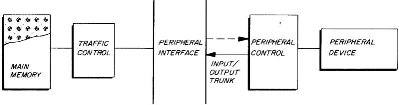
DIRECT ADDRESSING
When direct addressing is used, the variant character of the instruction word is zero.
Di-rect addressing means that the address field contains the absolute main memory address of the
operand. Accordingly, the address field is loaded directly into the address register, the operand
so addressed is retrieved, and the instruction is executed.
INDEXED ADDRESSING
When indexed addressing is used, the variant character of the instruction word has a value
from one to six, specifying one of the six 21-bit index registers. In this case the contents of the
address field are augmented by the contents of the specified index register. The contents of the
address field and the index register are not altered. The resulting sum is the absolute machine
address of the operand; the operand so addressed is retrieved and the instruction is executed.
FETCH INDIRECT -ADDRESS WORD
n=7
FETCH THE INSTRUCTION
n=0
I~ n!:.6 (XRn)+ X =
~---1~ effective address
EXECUTE INSTRUCTION
[image:21.618.64.566.372.675.2]SECTION IV. ADDRESSING
INDIRECT ADDRESSING
When indirect addressing is used, the variant character of the instruction word is seven.
Indirect addressing means that the address field contains not the absolute main memory address
of the operand but the address of a main memory location containing another address. The
con-tents of the location specified by the address field of the instruction word are retrieved. The
variant character of the word at that address has the normal meaning but is located at the
high-order end of the word to allow a 21-bit address field.
If the variant character of the indirectly addressed word is zero, bits 4 through 24 of the
word are interpreted as the absolute addres s of the operand. This addres s is loaded directly into
the address register, the operand so addressed is retrieved, and the instruction is executed.
If the variant character of the indirectly addressed word is seven, the addressing is
multi-level indirect. The procedure for indirect addressing is repeated until a word is addressed whose
variant character is not octal seven. This feature is represented by the loop in the flow chart in
Figure 3.
INDIRECT INDEXED ADDRESSING
If the variant character of the indirectly addressed word has a value from one to six, the
addressing is indirect indexed. That is, the 21-bit contents of the address field of the addressed
word are augmented by the contents of the index register specified by the variant character. The
instruction is then executed, using the operand addressed by the resulting sum.
EXPANDED MEMORY ADDRESSING
For systems with more than 32,768 words of memory, there is additional logic which
in-cludes a bank regis ter, additional bits in the sequence register, and three additional ins tructions.
The memory is handled in banks of 32,768 words. The additional bits in the sequence register
and those of the bank register are used to specify which bank is being addressed. The instructions
are divided into two sets: those whose address field normally references data (e. g., ADD, LDA)
and those whose address field normally references the sequence register (e. g., JMP, JAZ).
Instructions that reference the sequence register retrieve the bank indicator from the sequence
register; those that reference data take their bank indicator from the bank register.
The bank indicator in the sequence register is changed by normal incrementing or by
exe-cution of a Jump instruction with indirect or indexed addressing. The bank register is changed
by means of the optional instructions Load Bank Register (LBR) and Equalize Bank Register (EBR).
Effective addresses for instruction execution are derived from the appropriate bank
indi-cating register. The instructions themselves are taken from the bank specified by the bank
indi-cator bits of the sequence register. If direct addressing is used, the bank indicator is taken from
the appropriate bank indicating register. If indirect addressing is used, the bank indicator is
taken frOUl the indirectly addressed word. If indexed addressing is specified, the effective
ad-dress is computed from the sum of the contents of the index register, the low-order 15 bits of the
,
SECTION V
STANDARD INSTRUCTIONS
GENERAL SPECIFICATIONS
The following considerations apply to both the standard and the optional instructions (see
Section VI).
Execution Timing
The execution time represents the time required to retrieve the instruction, execute it, and
store the result. The following rules apply to the timing of instructions and should be used in
conjunction with the timing formulas in the text. If only one tirn.ing forrn.ula is given for an
in-struction, the execution tirn.e is the sarn.e with and without interlace.
1. For conditional jurn.p or skip instructions, the shorter tirn.e applies when the jurn.p or s kip is not rn.ade.
2. Indexed addressing requires, at rn.ost, an additional one-half cycle.
3. Indirect addressing requires one extra cycle per iteration.
Execution times are given in main mern.ory cycles, where one cycle equals 1.75 microseconds.
Indicators
OVERFLOW INDICATOR. This indicator denotes the occurrence of twos -complern.ent
over-flow of the accumulator. Overover-flow occurs when the precision of the fixed-point word is exceeded.
This indicator is cleared (reset) upon being tested by an SKN instruction.
CARRY INDICATOR. The carry indicator stores the true binary carry frorn. the high-order
position of the 24-bit accurn.ulator. This indicator is not cleared by being tested; instead, it
always indicates whether the result of the last operation that involved the accurn.ulator produced
a carry.
No-Address Instructions (NAD)
There is a group of instructions all of which have the sarn.e operation code (NAD). Instead
of specifying the addressing rn.ode, the variant character is used to differentiate these
instruc-tions. The variant characters and the corresponding rn.nern.onic operation codes are as follows:
Octal Variant
o
Mnern.onic Oper ation Code
Octal Variant
2 3 4 5
6
7
Mnemonic Oper ation Code
ALR SKN SKC STE SKE SRB
The PAS, EBR, and LBR instructions are differentiated by means of bits in the address field of
the instruction word.
Regis ters
The contents of control memory registers in the central processor rerrlain unchanged
during the execution of an instruction unless otherwise specified.
Symbology
The following symbology is used to describe H-300 instructions:
1.
2.
3. 4.
A
B
SR
( )
the accumulator.
the auxiliary arithmetic (B) register.
the sequence regis ter.
the contents of the location(s} indicated within the parentheses. For example, (SR) means "the contents of the sequence register. I!
5. Lower-case letters represent information that must be supplied by the progr ammer.
6. Upper-case letters and all digits and special characters except ellipsis (dots indicating progression) are coded literally in the position indicated. For example, digits appearing in the diagram of an instruction word must be coded literally in the positions shown for proper execution of the instruction. Thus, bits 7 through II of the Pass instruction (page 22) must be zero.
CONTROL INSTRUCTIONS
BAR - Branch and Return
6 7 9 10 24
(SR) replace (x). Then the address x+l replaces (SR) and the instruction at that address
CONTROL INSTRUCTIONS
By storing (SR), this instruction provides the option of perforITIing a subroutine beginning at
x+1 and then returning to the main sequence by jun1.ping indirectly to x.
Timing. 2 cycles.
EXC - Execute
I
OP CODE6 7 9 10 24
The instruction at location x is executed out of sequence. That is, (SR) are not altered.
The address of the next instruction is (SR).
Timing. I cycle plus the time required to execute the addressed instruction.
HT J - Halt Jump
I
OP CODE6 7 9 10 24
(x) replace (SR). Then the central processor halts.
Timing. I cycle.
JAN - Jump on Accumulator Negative
I
OP CODE6 7 9 10 24
The main memory address x replaces (SR) if the (A) are less than zero (i. e., if the high-order bit is one); else (SR) are incremented by one.
JAP - Jump on Accumulator Positive
The main memory address x replaces (SR) if (A) are equal to or greater than zero; else
(SR) are incremented by one.
Timing. 1 or 2 cycles.
JAZ - Jump on Accumulator Zero
I
OP CODEI :
v:
I : : : : : :
x: : : : : : : :
I
I 6 7 9 10 24
The main memory address x replaces (SR) if (A) equal zero; else (SR) are incremented
by one.
Timing. 1 or 2 cycles.
JMP - Jump
I
OP CODEI :
v:
I : : :
j : j:x: : :
j : I : II 6 7 9 10 24
The address x replaces (SR) unconditionally.
Timing. 1 cycle.
PAS - Pass (NAD)
I
OP CODE6 7 9 10 24
No operation. (SR) are incremented by 1.
CONTROL INSTRUCTIONS
SKM - Skip if Accumulator and Memory are Equal
I
OP CODE6 7 9 10 24
If (A) equal (x), (SR) are incremented by two (thus the next instruction is skipped); else
(SR) are incremented by one.
Timing. 2 or 3 cycles. With interlace: 1 or 2 cycles.
SKN - Skip if Signal is Not Set (NAD)
I
OP CODE6 7 9 10 24
Each I-bit in the address field x specifies an internal test point tobe sensed. If any of the test
points that are sensed is not set, (SR) are incremented by two (thus the next instruction is skipped);
else (SR) are incremented by one. Any combination of test points maybe sensedwithone SKN
instruction. The internal test points are:
Overflow Carry
Sens e Switch
#
1 Sens e Switch # 2 Sense Switch #3 Sense Switch #4Timing. 2 cycles.
SMZ - Skip if Memory is Zero
I
OP CODESense Switch #5 Sense Switch #6 Exponential Overflow Exponential Underflow Division Overcapacity
I :
v:
I : : : : : :
:x: : : : : : :
6 7 9 10 24
If (x) equal zero, (SR) are incremented by two (thus the next instruction is skipped); else
(SR) are incremented by one.
FIXED-POINT INSTRUCTIONS
ADD - Add to AccunlUlator
I
OPCODE
l:v:I:::::~:::::::
I
6 7 9 10 24
(A) are added to (x). The sum replaces (A).
Indicators. Overflow, carry.
Iinling. 2 cycles. With interlace: 1. 5 cycles.
ADM - Add to 1,1emory
6 7 9 10 24
(A) are added to (x). The sum replaces (x). (A) are not altered.
Indicators. None. The current contents of the overflow and carry indicators are not
altered.
Iiming. 3 cycles. With interlace: 2.5 cycles.
SUB - Subtract from Accumulator
I
OPCOD:r:I : :
I : : ; : : : : : : :I
I 6 7 9 10 24
(x) are subtracted from (A). The difference replaces (A).
Indicators. Overflow, carry.
FIXED-POINT INSTRUCTIONS
TLY - Tally
I
OP CODEI
:V:
I: : : :: :
7:
: : : : : I
6 7 9 10 24
(x) are incrernented by one. The Burn replaces (x).
Timing. 3 cycles. With interlace: 2.5 cycles.
INDEXING INSTRUCTIONS
Indexing instructions are those that manipulate the contents of general purpose register 0
or the contents of one of the six index registers. The desired register is specified by the variant
character of the instruction word as follows:
Octal
Variant Register
0 General Purpose Register 0
Index Register #1
2 Index Register #2
3 Index Register #3
4 Index Register #4
5 Index Regi s ter #5
6 Index Regis ter #6
7 Indirect Addres sing
Note that a variant character of zero does not specify direct addressing.
For indexing instructions, the effective address (i. e., x in the specifications) is the
con-tents of the address field of the first non-indirectly addressed word (namely, the first word
whose variant character is not 7).
Indexing ins truc tions c an be divided into two clas s e s depending on whether they us e the
effective address itself or the contents of the location specified by that address. They are
desig-nated as class I and class II indexing instructions, respectively. Class I instructions are DJX,
JIX, and STX; these instructions use x and not (x). Class II instructions are AUX, LDX, and
Clas s I Indexing Ins truc tions
DJX - Decrement and Jump on Index Not Zero
I
OP CODE6 7 9 10 24
The contents of register v are decremented by one. The result replaces the contents of
that register. Then if the contents of that register are not zero, the address x replaces (SR);
else (SR) are incremented by one.
Timing. 2 cycles.
JIX - Jump on Index Not Zero
I
OP CODEI :
v:
I : : : : : : :
x: : : : : : :
I
I 6 7 9 10 24
The address x replaces (SR) if the contents of register v are not zero; else (SR) are
incre-mented by one.
STX - Store Index Register
I
OP CODE6 7 9 10 24
The contents of register v replace (x).
INDEXING INSTRUCTIONS
Class II Indexing Instructions
A UX - AugITlent Index
I
OP CODEI :
v:
I : : : : : :.
I : : : : : : :I
I 6 7 ' 9 10 24
(x) are added to the contents of register v. The SUITl replaces the contents of that register.
TiITling. 2 cycles. With interlace: 1 cycle.
LDX - Load Index Register
I
OP CODEI :
v:
I : : : : : :
x: : : : : : : :
II 6 7 9 10 24
(x) replace the contents of register v.
TiITling. 2 cycles. With interlace: 1 cycle.
SKX - Skip on Index High
I
OP CODE6 7 9 10 24
If the contents of register v are greater than (x), (SR) are increITlented by two (thus the
next instruction is skipped); else (SR) are increITlented by one.
INPUT !OUTPUT INSTRUCTIONS, DIRECT
PIN - Peripheral Input
I
OP CODE6 7 9 10 24
If the device connected to the input bus is not ready, the next instruction in sequence is
executed; else the 24-bit word on the input bus replaces (x), and (SR) are incremented by two
(thus the next ins truc tion is skipped).
Timing. 3 cycles. With interlace: 2 cycles.
POT .- Peripheral Output
I
OP CODEI :
v:
I : : : : : :.: :: ::::
I
6 7 9 10 24
If the device connected to the output bus is not ready, the next instruction in sequence is
executed; else (x) are transferred to the output bus and (SR) are incremented by two (thus the
next instruction is skipped).
Timin~. 3 or 4 cycles. With interlace: 2 or 3 cycles.
SKC - Control and Skip (NAD)
6 7 9 10 18 19 24
This instruction interrogates and controls peripheral devices by way of peripheral controls
attached to the direct input/output channel. If a positive response is received, (SR) are
incre-mented by one; if a negative response or no response is received, (SR) are increincre-mented by two
(thus the next instruction is skjpped).
The commands that may be directed to the keyboard printer, the paper tape reader, and the
INPUT /OUTPUT INSTRUCTIONS, DIRECT
Test the addressed device for an interrupt signal. Test the addressed device for a stored error condition. Test the addressed device for a busy condition.
Start the addressed device. Stop the addressed device.
Timing. 2 cycles.
,
SKE - Skip if External Signal is Not Set (NAD)
I
OP CODE6 7 9 10 24
Each 1 -bit in the address field x specifies one of 15 external sensing lines to be tested.
If all of the lines that are tested are set (carry a logical 1), (SR) are incremented by one; else
(SR) are incremented by two (thus the next instruction is skipped). The status of the sensing lines
is not altered.
Timing. 1 or 2 cycles.
STE - Set External Point (NAD)
I
OP CODE6 7 9 10 24
Each 1 bit in the addres s field x causes a pulse to be sent over one of 15 external acbvating lines.
Timing. 1 cycle.
INTERRUPT INSTRUCTIONS
LIM - Load Interrupt Mask
I
OP CODE: : :x" : : : : : :
I
6 7 9 10 24
(x) replace the contents of the interrupt mask register.
SRB - Set/Reset Interrupt Block {NAD}
6 7 9 10 24
If parameter a {the low-order bit of the address field} is one, the interrupt block is set,
blocking all peripheral interrupts. If parameter a is zero, the interrupt block is cleared,
enabling all peripheral interrupts; in this case the next instruction in sequence will be under way
before the status change occurs and is therefore not interrupted.
Timing. 1 cycle.
STI - Store Interrupt Register
CODE I
:V:
I : : : : : : :
x: : : : : : :
I
6 7 9 10 24
The contents of the interrupt register replace {x} and are not altered.
Timing. 2 cycles. With interlace: 1 cycle.
XML - Exchange Interrupt Mask
CODE
I:v I:
::: x: : : : : : : :
I
6 7 9 10 24
The contents of the interrupt mask register are exchanged with {x}.
LOGIC INSTRUCTIONS
LOGIC INSTRUCTIONS
EXT - Extract (Logical AND)
I
OP CODEI :
V:
I : : : : : : :
x: : : : : : :
I
6 7 9 10 24
(A) logical-AND (x) replace (A). That is, if corresponding bits in (A) and (x) are both one,
a one replaces the bit in (A); else a zero replaces the bit in (A). (x) are unchanged. Hence the
following truth table:
(A) AND (x) GIVING (A)
o
0 0o
1 0o
0Timing. 2 cycles. With interlace: 1 cycle.
HAD - Half Add (Exclusive OR)
I
OP CODEI :
v:
I : : : : : :
:x: : : : : : :
I
6 7 9 10 24
(A) exclusive-OR (x) replace (A). That is, if corresponding bits in (A) and (x) are not
identical, a one replaces the bit in (A); else a zero replaces the bit in (A). Hence the following
tru th table:
(A) OR (x) GIVING (A)
o
o
o
1
o
1
Timing. 2 cycles. With interlace: 1 cycle.
o
1
SECTION V. STANDARD INSTRUCTIONS
SMP - Superimpose (Inclusive OR)
I
OP CODEI :
V:
I : : : : : ::x: : : : : : :
I
6 7 9 10 24
(A) inclusive-OR (x) replace (A). That is, if corresponding bits in either (A) or (x), or
both, are one, a one replaces the bit in (A); else a zero replaces the bit in (A). Hence the follow.
ing truth table:
(A) OR (x) GIVING (A)
o
a
a
I
o
I
Timing. 2 cycles. With interlace: I cycle.
a
I I I
SST - Substitute
I
OP CODEI :
v:
I : : : : : :
X: : : : : : : :I
6 7 9 10 24
For corresponding bit positions in (A), (B), and (x), if the bit in (B) is one, the bit in (A)
replaces the bit in (x); else the bit in (x) is protected. Thus, (B) are a mask. Hence the following
truth table:
(A) (B) (x) GIVING (x)
a
0a
00
a
a
I 0a
a
Ia
I
a
a
a
I
a
011
a
1 1
SHIFT INSTRUCTION
SHIFT INSTRUCTION
SFT - Shift (NAD)
I
OP CODE6 7 9 10 18 19 24
(A), or, if double precision is specified, (A, B) are shifted n places to the left or right in the rotate or arithmetic mode. In a left arithmetic shift, zero replaces each of the emptied
positions. In a right arithmetic shift, the high-order bit of (A) is duplicated in each of the emptied positions.
PARAMETER
d
m
p
n
3n Timing. 1
+7 .
INTERPRET A TION
Direction Indicator
Left shift if d is O.
Right shift is d is 1.
Mode Indicator
Rotate if m is O. Bits moved off the end of the word(s) are transferred end- around to the other end of the word( s).
Arithmetic if m is 1. Bits moved off the end of the word(s) are lost.
Precision Indicator
Single precision if p is O. Only (A) are operated upon.
Double precision if p is 1. (A, B) are operated upon. Number of binary places to be shifted.
WORD TRANSMISSION INSTRUCTIONS
ALR - Alter Register (NAD)
I
OP CODE6 7 9 10 24
specified by the destination address d, under control of parameter ad' replace the content of the
register specified by the source address s. If d = s, the contents of the register so specified are
altered as specified by as. The control memory regis ters are addres sed as follows:
Regis ter Octal Addres s
Gene r al- Purpo s e Regis ter 0 00
Index Register I 01
Index Register 2 02
Index Register 3 03
Index Regis ter 4 04
Index Regis ter 5 05
Index Register 6 06
A Register (Accumulator) 07
Gene r al- Pu r po s e Register 10
General-Purpose Register 2 I I
General-Purpose Register 3 12
General-Purpose Register 4 13
General-Purpose Register 5 14
General-Purpose Register 6 15
General-Purpose Register 7 16
B Register (Auxiliary Arithmetic Register) 17
PARAMETER INTERPRETATION
t
d
s
Transfer Mode
One-way transfer within control memory if t is O. The contents of the source register s replace the contents of the destination register d as specified by as.
Exchange within control memory is t is 1. The contents of the source register s replace the contents of the destination register d as specified by as. Also, the contents of the destination register d replace the contents of the source register s as specified by ad.
One-way transfer from the counters associated with the read/write channels if t is 2.
Alter Mode for Destination Register
Transfer the contents unaltered if ad is O.
Transfer the twos -complement of the contents if ad is 1.
Transfer the absolute value of the contents if ad is 2.
Destination address. Address of a con'trol memory register.
Alter mode for source register. Same options as for ad.
Source address. Address of a control memory register.
WORD TRANSMISSION INSTRUCTIONS
DLD - Double-Precision Load
I
OP CODEI :
v:
I :.: : : : :
:x: : : : : : :
I
I 6 7 9 10 24
(x) replace (A); (x+l) replace (B').
Timing. 3 cycles. With interlace: 2 cycles.
DST-Double-Precision Store
lOp
COD EI :
v:
I : : : :
I:x: : : : : : : :
I
I 6 7 9 10 24
(A) replace (x); (B) replace (x+l).
Timing. 3 cycles. With interlace: 2 cycles.
LDA - Load Accumulator
I
OP CODEI :
v:
I : : : : :
:x : : : : : : : :
II 6 7 9 10 24
(x) replace (A).
Timing. 2 cycles. With interlace: 1 cycle.
LDB - Load B Register
I
OP CODEI
:v:
I :
I : : I : : :I 6 7 9 10 24
MTR - Multiple Transfer
I
OP CODE [ :V: [ : : : : : :
:x: : : : : : :
I
I 6 7 9 10 24
I
w6 7 9 10 24
Starting with (x), w words (0 ~ w $ 63) are transferred to consecutive main memory lo-cations starting with address a. The addresses x and a have independent variant characters.
This is a two -word ins truction.
Timing. 2.5
+
2w cycles. With interlace: 3.5+
w cycles.STA - Store Accumulator
I
OP CODEI :
v:
I : : : : : :~
: : : : : : :I
I 6 7 9 10 24
(A) replace (x).
Timing. 2 cycles. With interlace: 1 cycle.
STB - Store B Register
I
OP CODEI :
v:
I : : : : : : :
X: : : : : : :
I
6 7 9 10 24
(B) replace (x).
WORD TRANSMISSION INSTRUCTIONS
ST Z - Store Zeros in Memory
I
OP CODE I :V:
I : : : : : ::x: : : : : : :
I
1 6 7 9 10 24
24 zeros replace {x}.
Four categories of optional instructions are available with the H- 300. The character
instructions permit manipulation of i'ndividual characters within words while protecting the rest
of the addres sed word. The multiply/ divide instructions, either by themselves or together with
the floating-point instructions, increase the power of the system in scientific applications. The
expanded memory instructions are included in all systems having more than 32,768 words of
memory.
All systems include the hardware bypas s feature: use of an optional instruction which is
not installed in the machine causes a subsequence to a fixed memory location. The program
there may identify the instruction and execute it by means of a subroutine.
CHARACTER INSTRUCTIONS
The character instructions interpret the H- 300 main memory word as four alphanumeric
(six-bit) characters. The low-order two bits, shown below as bits n, specify which of the four
characters is to be used, counting from left to right in the addressed word.
The high- order bit of the variant character, shown below as bit v, specifies one of two
available addressing modes. If the bit is zero, it specifies direct addressing; else it specifies
indirect addressing.
CSK - Characters Skip if Equal
I
OP CODEIv I
~
I : : : : : :
:x
::
: : :
I
6 7 9 10 24
(SR) are incremented by two if character n in (A) equals character n in (x) (thus the next
instruction is skipped); else (SR) are incremented by one.
SEC TION VI. OPTIONAL INSTR UC TIONS
LCH - Load Character
I
OP CODE IVI
~
I : : : : : : :.: : : : : : :
I
I 6 7 9 10 24
Character n of \x} replaces character n of (A). The other characters of (A) are unchanged. Timing. 2 cycles. With interlace: 1 cycle.
SCH - Store Character
I
OP CODEH": I : : : : : : :.: : : : : : :
II 6 7 9 10 24
Character n of (A) replaces character n of (x). The other characters of (x) are unchanged. Timing. 2 cycles. With interlace: 1 cycle.
EXPANDED MEMORY INSTRUCTIONS
EBR - Equalize Bank Register (NAD)
The contents of the bank indicator in the sequence register replace the contents of the bank
register. Thus the contents of the sequence register bank indicator and the bank register are
equalized.
Timing. 1 cycle.
LBR - Load Bank Register
I
OP CODE6 7 9 10" 12 24
The contents of the bank-bit field of the instruction word replace the contents of the bank
SBR - Store Bank Register
I
OP CODE x6 7 9 10 24
The contents of the bank register replace the low-order portion of (x). The rest of (x)
is protected. The format of (x) is compatible with the Load Bank Register (LBR) instruction.
Timing. 2 cycles.
MULTIPLY /DIVIDE INSTRUCTIONS
DIV - Divide
I
OP CODEI : v:
I : : : : : :
x: : : : : : : :
I
6 7 9 10 24
(A, B) are treated as a 48- bit dividend and divided by (x). The quotient replaces (A).
The remainder replaces (B).
Indicators. Division overcapacity.
Timing. 12 cycle s.
MPY - Multiply
I
OP CODEI :
v:
I : : : : : : :x: : :: : : :
I
6 7 9 10 24
(A) are multiplied by (x). The product replaces (A, B) taken as a 48- bit register.
Timing. 4 cycles.
FLOATING-POINT INSTRUCTIONS
This set of instructions provides a complete floating-point repertoire for the H-300. The
SECTION VI. OPTIONAL INSTRUCTIONS
The variable N in the timing formulas in this section represents the number of shifts
re-quired to justify the operands and/ or to normalize the result.
FAD - Floating Add
I
OP CODEI :
v:
I : : : : :
:x: : : : : : : :
I
6 7 9 10 24
(A, B) are treated as one 48- bit register, as are (x, x+ I). The two operands are justified
and then added together. The normalized sum replaces (A, B). An operand can be normalized
by adding it to a floating-point zero.
Indicators. Exponential overflow and underflow.
Timing. 4
+
7""
N cycles.FDV - Floating Divide
I
OP CODE: x:: :::::
I
6 7 9 10 24
(A, B) are treated as one 48- bit register, as are (x, x+l). (x, x+l) are divided into (A, B).
The quotient replaces (A, B). The operands are not justified and the quotient is not normalized.
The remainder can be retrieved by means of the Floating Unload instruction (see pag.e 43).
Indicators. Exponential overflow and underflow.
Timing. 26 cycles.
FMP - Floating Multiply
I
OP CODEI :
v:
I : : : : : :
x: : : : : : : :
I(x, x+l). The normalized high-order product replaces (A, B). The low-order product can be
retrieved by means of the Floating Unload instruction (see below).
Indicators. Exponential overflow and underflow.
Timing. 9 +
'"7
N cycles.FSB - Floating Subtract
I
OP CODEI :
v:
I : : : : : :
:x: : : : : : :
I
6 7 9 10 24
(A, B) are treated as one 48- bit register, as are (x, x+ 1). The two operands are justified
and (x, x+l) are subtracted from (A, B). The normalized difference replaces (A, B).
Indicators. Exponential overflow and underflow.
Timing. 4 +
'"7
N cycles.FUL - Floating Unload
I
OP CODEI :
v:
I : : : : : : : : : : : : : :
6 7 9 10 24
The floating-point low- order product or remainder replaces (A, B).
Timing. 4 cycles.
INPUT/OUTPUT INSTRUCTIONS, BUFFERED
The following instructions are used in conjunction with the optional read/write channels