Limitations of On-Wafer Calibration and De-Embedding
Methods in the Sub-THz Range
Manuel Potereau1, Christian Raya2, Magali De Matos1, Sébastien Fregonese1, Arnaud Curutchet1,
Min Zhang2, Bertrand Ardouin2, Thomas Zimmer1,2
1
IMS Laboratory, University of Bordeaux 1, Talence, France; 2XMOD Technologies, Bordeaux, France. Email: [email protected]
Received August 2013
ABSTRACT
This paper investigates frequency limitations of calibration and de-embedding techniques for S parameter measure-ments. First, the TRL calibration methods are analysed and the error due to the probe movement when measuring the different line lengths is quantified, next the coupling between the probe-heads and the wafer surface is investigated and finally an upper frequency validity limit for the standard Open-Short de-embedding method is given. The measured results have been confirmed thanks to the use of an electro-magnetic simulator.
Keywords: TRL; Open-Short; De-Embedding; Calibration
1. Introduction
The frequency range in electronic applications is con- tinuously increasing during the past few years to reach the range of hundreds of Gigahertz. The associated bipo- lar and CMOS transistors used as elementary compo- nents for these high frequency applications have maxi- mum oscillation frequency reaching the half Terahertz [1]. Hence, characterisation of advanced SiGeC HBT and CMOS devices and their associated passive elements are more and more challenging. First, different calibration techniques of the network analyser such as TRL and SOLT at frequency higher than 50 GHz need to be veri- fied. Moreover, associated device modelling requests accurate characterisation of the intrinsic device, e.g. free of parasitic elements such as pads, vias and interconnects. Hence, conventional de-embedding techniques such as Open-Short need to be refined for higher frequencies. It has already been shown that calibration and de-embed- ding techniques are less accurate when the frequency increases [2]. Some parasitic effects, formerly negligible, are now strong enough to modify significantly the S- parameters measurement [3,4]. This paper investigates three different errors that can commonly occur in Sub- THz measurements and which are mostly not taken into account: First, a practical limitation of the TRL technique is presented due to the measurements of different line lengths. Then, a second limitation of the calibration tech- nique due to the difference between the calibration sub- strate and the device under test structure is explored. Fi-
nally, a limitation of the conventional de-embedding Open-Short method is highlighted on active and passive elements.
2. Influence of the Probe Movement during
Measurement
The TRL calibration method is based on the measure- ment of three different standards:
• a reflect, which can be an open or a short and need to
be as symmetrical as possible
• a short line, (called through in the rest of the paper)
• a long line, (called line in the rest of the paper)
The TRL is based on the measurement of two lines with different lengths [5]. In between the measurements of these lines, one probe is moved as described on the top
of the Figure 1. When this probe is moved, the meas-
urement environment is altered at high frequency. For example, crosstalk between probes is reduced, the probe contact resistance can be changed and the position of the cable is slightly changed when moving the probe head. Due to these small modifications of the measurement environment the calibration is less accurate at high fre- quencies. Hence, we expose a method to quantify the error introduced by moving the probe head. A special test structure has been designed using two open structures
with different distances between the probes, see Figure
1.
Figure 1. Sketch of the probes movement front (up) and top view (down).
x-axis as shown by the white arrow on Figure 1. The
Open structure “B” is measured and then the two meas- urements are compared.
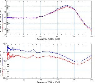
On the Figure 2, the admittance (y-parameter) and
capacitance for the right probe are shown. This probe is not moved between the two measurements.
The admittance is exactly the same for each measure- ment and the capacitance has the same behaviour, only an offset is visible.
Figure 3 shows the admittance and capacitance for the left port before (red curve) and after the probe movement (blue curve).
On this figure, the admittance’s maximum is shifted to
lower frequencies by 15 GHz and raised by 0.5 mS (~50%) between the two measurements. The graph also shows a modification in the behaviour of the test struc- ture’s electrical characteristic above 50 GHz. There is a drop in the capacitance value. This result is not-physical because the test structure is still the same!
As a conclusion, above 50 GHz, a probe movement can introduce measurement errors. This can be critical because the line measurement is one of the key-steps during TRL-calibration.
3. Coupling between Probes and Test
Structures under the Probes
Due to the cost of the silicon area, test structures are placed as close as possible to each other.
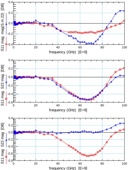
The RF probes are large compared to the pad size, and a part of the probes is right above the neighbouring structures. The structures under the probes make a strong coupling with the RF probes [3]. To quantify this cou- pling, we carried out the following measurements shown on Figure 4. The red and blue triangles are the RF probes in GSG configuration. The cell called “A” does not have any coupling under its left probe. The cell called “C” does not have any coupling under its right probe while the structure “B” is totally symmetric and has a coupling on both sides. The three measured test-struc- tures are identical and symmetrical (open). Consequently,
[image:2.595.148.454.448.716.2]the measured characteristics should be symmetrical (S11
Figure 2. Port 2 admittance (up) and capacitance (down) before and after left probe move.
frenquency (GHz) [E+9]
Y
1 c
el
l A
Y
1 c
el
l B
[
E
-3]
0 20 40 60 80 100
-1.5 -1.0 -0.5 0.0 0.5 1.0 1.5
frenquency (GHz) [E+9]
C
1 c
el
l A
C
1 c
el
l B
[
E
-15]
0 20 40 60 80 100
Figure 3. Port 1 admittance (up) and capacitance (down) before and after left probe move.
Figure 4. Placement of the measured test structures.
= S22). The difference that we can see is due to the cou-
pling between probe and the neighbour test structures under it.
The middle graph of the Figure 5 shows the coupling
between probes and test structures under it. Thanks to the symmetry of the structure, the behaviour of the two ports
of the cell “B” is completely symmetrical (S11 = S22).
On the top and bottom graph, we can see that the measurement is no longer symmetrical; this is due to the absence of test structures under the left probe for the first graph and under the right probe for the third one.
For on-wafer measurement, the coupling between
Figure 5. Measurement results for the cell A (up), B (mid-dle), C (down).
frenquency (GHz) [E+9]
Y
2 c
el
l A
Y
2 c
el
l B
[
E
-3]
0 20 40 60 80 100
-1.0 -0.5 0.0 0.5 1.0 1.5
frenquency (GHz) [E+9]
C
2 c
el
l A
C
2 c
el
l B
[
E
-15]
0 20 40 60 80 100
35.0 37.5 40.0 42.5 45.0
frequency (GHz) [E+9]
S
11 m
ag m
ag(
S
.m
.22)
[
D
B
]
0 20 40 60 80 100
-0.4 -0.2 0.0 0.2 0.4
frequency (GHz) [E+9]
S
11 m
ag S
22 m
ag [
D
B
]
0 20 40 60 80 100
-0.6 -0.4 -0.2 0.0 0.2 0.4
frequency (GHz) [E+9]
S
11 m
ag S
22 m
ag [
D
B
]
0 20 40 60 80 100
[image:3.595.312.538.406.706.2]probes and test-structures can be controlled by the inser- tion of dummies on the first and the last column of the chip. E.g. Single port calibration standards can be in- serted in those columns.
Another question arises here. Usually the calibration is done with an ISS-standard substrate. The surface of this calibration substrate is completely different compared to the wafer surface and consequently the coupling during calibration is different compared to the measurement. The only solution to correct for the coupling is to use on- wafer calibration structures and no longer use the ISS- standard.
4. Open-Short De-Embedding Limitation
During the high frequency measurement of a large multi-
finger transistor (HBT), the S11 (Figure 6) shows a non-
physical behaviour after the de-embedding with the Open-Short methodology (OS).
The impedance (represented by the magnitude of S11) is higher after the de-embedding (red line) because the losses (especially through the pads) are compensated. The Figure 6 also shows that the de-embedded magni- tude is increasing with frequency after 60 GHz which is not physical for the measured input impedance of the HBT. This non-physical behaviour is due to over com- pensation of the pad capacitance during de-embedding. In order to validate this hypothesis, EM simulation has
been carried out. The methodology is explained on Fig-
ure 7.
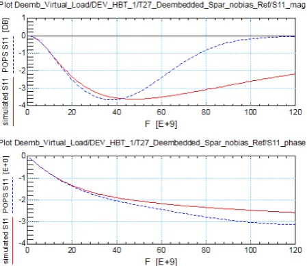
First, an inductance is simulated with HFSS without the back-end. From a technical point of view, when using an electromagnetic simulator, it is not possible to define a port near a discontinuity. A work-around was to add a short line, make the simulation of the whole structure and then to remove the short line using the standard de-em- bedding procedure. This is represented on the first line of the Figure 7.
In a second step, the same inductance is simulated
with the back-end (see second line of Figure 7). A Short
[image:4.595.315.534.473.588.2]and an Open are also simulated and the OS de-embed- ding is performed. The simulation results are shown on
Figure 8, upper part: magnitude, lower part: phase. The simulation results of the inductance without back- end are given by the red curve. The simulation results of
the inductance after OS de-embedding are given by the blue curve. Theoretically, a perfect superposition of the red and blue curves is expected, but a large difference appears above 40 GHz, especially for the magnitude. A similar increase of the magnitude in the high frequency range is visible as already before seen during measure-
ments (Figure 6, red line). We can conclude that above
60 GHz, the OS de-embedding introduces a non negligi- ble error.
For accurate measurements, a new de-embedding me- thod is needed. The 6 dummies method developed in [2] and [6] is highly recommended in this frequency range.
5. Conclusions
High frequency calibration and de-embedding techniques have been analyzed and their validity range has been checked: 1) the TRL calibration need the measurements of two different line lengths introducing the movement of the probe-heads for on wafer-measurements. This move- ment can introduce errors and make the calibration less precise above 40 GHz. 2) the coupling between the probe-heads and the underlying wafer-surface introduces an error when the structures on the wafer that are under the probe-heads are not identical. A work around is to pay particular attention when designing the test-struc- tures to take this effect into account.
The most widely used de-embedding technique (Open- Short) introduces major errors in measurement above 60 GHz. The 6 dummies method developed in [6] is highly recommended above this frequency range.
Figure 6. Magnitude (up) of a transistor S11 without OS (blue line) and after OS (red line).
[image:4.595.140.457.634.719.2]Figure 8. Simulation magnitude (up) and phase (down) of an inductance; intrinsic (red) and extracted with OS de- embedding (blue).
6. Acknowledgements
This work is part of the DotSeven project supported by the European Commission through the Seventh Frame- work Program for Research and Technological Devel- opment. The authors would like to thank STMicroelec- tronics for wafer supply.
REFERENCES
[1] P. Chevalier, F. Pourchon, T. Lacave, G. Avenier, Y.
Campidelli, L. Depoyan, G. Troillard, M. Buczko, D. Gloria, D. Céli, C. Gaquiere and A. Chantre, “A Conven- tional Double-Polysilicon FSA-SEG Si/SiGe:C HBT Reaching 400 GHz fMAX,” IEEE Bipolar/BiCMOS Cir- cuits and Technology Meeting, Capri, 12-14 October 2009, pp. 1-4.
[2] N. Derrier, A. Rumiantsev and D. Celi, “State-of-the-Art and Future Perspectives in Calibration and De-Embedding Techniques for Characterization of Advanced SiGe HBTs Featuring Sub-THz fT/fMAX,” 2012 IEEE Bipolar/ BiCMOS Circuits and Technology Meeting (BCTM), Portland, 30 September-3 October 2012, pp. 1-8.
[3] J. Bazzi, C. Raya, A. Curutchet and T. Zimmer, “Investi- gation of High Frequency Coupling between Probe Tips and Wafer Surface,” IEEE Bipolar/BiCMOS Circuits and Technology Meeting, Capri, 12-14 October 2009, pp. 87- 90.
[4] J. Bazzi, “Caractérisation des Transistors Bipolaires à Hétérojonction SiGe à très Hautes Fréquences,” Ph.D. Thesis, University of Bordeaux 1, Bordeaux, 2011.
[5] J. P. Mondal and T.-H. Chen, “Propagation Constant Determination in Microwave Fixture De-Embedding Pro- cedure,” IEEE Transactions on Microwave Theory and Techniques, Vol. 36, No. 4, 1988, pp. 706-714,.
[image:5.595.62.287.88.282.2]