© 2016, IRJET | Impact Factor value: 4.45 | ISO 9001:2008 Certified Journal | Page 337
Implementation of UART with BIST Technique
Mr.S.N.Shettennavar
1, Mr.B.N.Sachidanand
2, Mr.D.K.Gupta
3, Mr.V.M.Metigoudar
4 1, 2, 3,4Assistant
Professor
,Dept. of Electronics Engineering, DKTE’s Textile and Engineering Institute
Ichalkaranji Maharashtra India.
---**---
Abstract:
Asynchronous serial communication is usually implemented by Universal Asynchronous Receiver Transmitter (UART), used for short distance, low speed, low cost data exchange between processor and peripherals. There is a need for realizing the UART function in a single or a very few chips due to VLSI Testing problems like test pattern generation, input combinatorial problems, and gate to I/O pin ratio problems. Designing systems without full testability are open to the increased possibility of product failures and missed market opportunities.It is a need to ensure the data transfer is error proof. This project introduces Status Register and BIST (Built-In-Self-Test) to overcome the testability and data integrity. With Implementation of BIST, expensive tester requirement and testing procedures starting from circuit or logic level to field level testing are minimized. LFSR replaces function of external tester by automatically generating pseudo random patterns to give good fault coverage to UART module. Hence overall production cost is reduced.
Result of this project is compared with reference paper [8] providing number of CLBs, LUTs, Bonded I/Os used by Spartan3 is 38, 54, 19 and simulation time 9.668ns. It indicates improvement in area from 8.667% to 6.334% and overall 2.33% area reduction. Simulation time (delay) is reduced from 9.668 ns to 7.498 ns overall 2.170 ns reduction in delay.
Keywords: UART, BIST, LFSR, Simulation and Synthesis.
1. INTRODUCTION
UART (Universal Asynchronous Receiver Transmitter) is an asynchronous serial communicating device used for data exchange between processor and its peripherals [1]. UART allows full-duplex communication in serial link, thus has been widely used in the data communication and control system applications.
UART communication needs only two signals (Transmit, Receive) to complete full-duplex data communication [2]. UART includes three modules namely, the baud rate generator, receiver and transmitter. The baud rate generator is used to produce a local clock signal which is much higher than the baud rate to control the UART receive and transmit; The UART receiver module is used to receive the serial signals at RXD, and convert them into parallel data; The UART
transmit module -converts the bytes into serial bits according to the basic frame format and transmits those bits through TXD.
Initially transmitter is idle; the Txout line is in the high logic state. Otherwise when a word is given to the UART for asynchronous transmissions, “start bit” (logic low) is added to the beginning of each word that is to be transmitted. The start bit is used to alert the peripheral receiver that a word of data is about to be sent and to force the clock in the receiver into synchronization with the clock in the transmitter. After the start bit, the individual data bits of the word are sent, with the Least Significant Bit (LSB) being sent first. Each bit is transmitted for exactly the same amount of time as all of the other bits and the receiver samples at the wire at approximately half way through the period assigned to each bit to determine if the bit is a 1 or a 0. When the entire data word has been sent, the transmitter adds a parity bit that the transmitter generates. The Parity Bit may be used by the receiver to perform simple error checking. Then at least one Stop Bit is sent by the transmitter to indicate current data is transmitted successfully and next data can be loaded for transmission [4].
When the receiver has received all of the bits in the frame, it automatically discards the Start, Parity and Stop bits. If another word is ready for transmission, the Start bit for the new word can be sent as soon as the Stop bit for the previous word has been sent. Asynchronous data are “self synchronizing” if there are no data transmit, the transmission line is held idle [5].
Manufacturing processes are extremely complex, inducing manufacturers to consider testability as a requirement to assure the reliability and the functionality of each of their designed circuits [3], [7]. Testing of integrated
© 2016, IRJET | Impact Factor value: 4.45 | ISO 9001:2008 Certified Journal | Page 338
not easily observed at output pin (Observability).Henceexternal diagnostic capability is employed to test such complex core circuits.
In this paper, internal diagnostic capabilities are built into UART by the introduction of Built-In-Self-Test (BIST)[3] and error simulation of data at receiver for any data corruption and thereby setting status flags [1]. The UART with status register and BIST module is coded in Verilog HDL and simulated using Xilinx tool ISESIM. The complete implementation and validation is done on Spartan 3A FPGA.
The paper is organized into 5 sections. Section 2 explains BIST technique and implementation possibilities. Section 3 explains the architecture of UART with introduction of BIST technique. Section 4 presents them results and section 5 provides the conclusion of work.
2. BIST TECHNIQUE
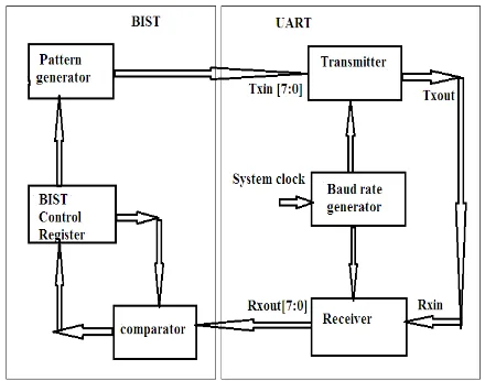
VLSI testing problems like Test generation problems, input combinatorial problems, gate to I/O pin ratio problems are discussed [3] and this motivated designers to identify reliable test methods in solving these difficulties. An insertion of special test circuitry on the VLSI circuit that allows efficient test coverage is the answer to the problem. It is addressed by the need of design for testability (DFT) using BIST circuit. BIST is an on-chip test logic that is utilized to test the functional logic of a chip, by itself. With the rapid increase in the design complexity, BIST has become a major design consideration in DFT methods and is becoming increasingly important in today’s state of the art SoCs. A properly designed BIST is able to offset the cost of added test hardware while at the same time ensuring the reliability, testability and reduces maintenance cost. BIST solution consists of an Automatic Test Pattern Generator (ATPG), the circuit to be tested, a way to analyze the results, and a way to compress those results for simplicity and handling. Fig. 1 shows a BIST module composition. Generic BIST architecture components [7] are;
Circuit under Test (CUT): This is the portion of the circuit tested in BIST mode. It can be sequential, combinational or a memory. It is delimited by their Primary Input (PI) and Primary Output (PO).
Test Pattern Generator (ATPG): It generates the test patterns for the CUT. It is a dedicated circuit or a microprocessor. The patterns may be generated in pseudorandom or deterministically. Normally, the pattern generator generates exhaustive input test patterns to the CUT to ensure the high fault coverage. For example, a CUT with 10 inputs will require 1024 test patterns.
Test Response Analysis (TRA): It analyses the value sequence on PO and compares it with the expected output.
BIST Controller Unit (BCU): It controls the test execution; it manages the ATPG, TRA and reconfigures the CUT and the multiplexer. It is activated by the Normal/Test signal. During BIST mode, it selects input from the pattern generator to CUT while during functional mode, selects primary inputs.
Fig-1: General BIST Module
The following hardware pattern generation approaches have been used.
1. ROM. One method is to store a good test pattern set (from an ATPG program) in a ROM on the chip, but this is prohibitively expensive in chip area.
2. Binary Counters. A binary counter can generate an exhaustive test sequence, but this can use too much test time if the number of inputs is huge
3. Modified Counters. Modified counters have also been successful as test-pattern generators, but they also require long test sequences
4. Linear Feedback Shift Register (LFSR) to generate pseudo-random tests. This frequently requires a sequence of 1 million or more tests to obtain high fault coverage, but the method uses very little hardware and is currently the preferred BIST pattern generation method.
5. LFSR and ROM. One of the most effective approaches is to use an LFSR as the Primary test mode, and then generate test patterns with an ATPG program for the faults that are missed by the LFSR sequence. These few additional test-patterns can either be stored in a small ROM on the chip for a second test approach, they can be embedded in the output of the LFSR, or they can be embedded in a scan chain in order to augment the stuck fault coverage to 100%.
6. Cellular Automaton. In this approach, each pattern generator cell has a few logic gates, a flip-flop, and connections only to neighboring gates. The cell is replicated to produce the cellular automaton.
3. PROPOSED UART ARCHITECTURE WITH
BIST
© 2016, IRJET | Impact Factor value: 4.45 | ISO 9001:2008 Certified Journal | Page 339
to monitor the correctness of every received data byteand enhance the testability of circuit by the introduction of BIST module. The hardware architecture of the 8-bit UART with Status register, incorporated with BIST module is explained in the following sections.
The proposed model has two major modules viz. UART and BIST. Further in the UART, we have transmitter, receiver, and baud rate generator. Baud rate generator works at 50 MHz and further reduced as required for the operations in transmitter and receiver to achieve baud rate of 9600 bps. BIST has a control register, pattern generator and a Comparator, as shown in fig-2.
Fig -2: UART with BIST architecture
3.1. Transmitter:
The transmitter accepts parallel data from peripheral/ processor makes the frame of the data and transmits the data in serial form on the transmitter output (Txout) terminal figure 3. The baud rate generator output will be clock for UART transmitter.
Data is loaded from the parallel inputs Txin0-Txin7 into the transmitter FIFO by applying logic high on the WR (Write) input. FIFO is 16 byte register. If FIFO is full it sends FIFO full (FF) signal to peripheral as shown in fig-3.
3.1.1.
Transmitter Operation
The flow chart shown in fig-5 explaining transmission of serial data from FIFO to transmitter output. When FIFO contains some data it will send the signal to transmitter hold Register (THR), which is an 8 bit register. At the same time if THR is empty it will send the signal to FIFO which indicates that THR is ready to receive data from FIFO. If the Transmitter Shift Register (TSR) is empty it will send the signal to THR and it indicates that TSR is ready to receive data from the THR. TSR is an 11 bit register in which framing process occurs. In frame Start bit, parity bit and Stop bit are added as shown in fig-4. Parity bit is generated by XORing the data bits of THR register. Now data is
transmitted from TSR to TXOUT serially one bit at time with help of finite state machine (FSM) as shown in fig-6.
Fig- 3: Transmitter
Fig-4: UART Frame Format
Fig-5 Transmitter flowchart – FIFO to TXOUT
Fig-6:
Transmitter state diagram
3.2. Receiver
: [image:3.595.315.556.137.530.2] [image:3.595.39.259.259.432.2] [image:3.595.332.512.532.683.2]© 2016, IRJET | Impact Factor value: 4.45 | ISO 9001:2008 Certified Journal | Page 340
least significant bit and collectively provides the serialdata of 8 bit. When the load signal is high it will get the start bit from the transmitter which assures that the original data is now being send by the transmitter. Once the shift signal is becomes high with no load signal, the data coming from the transmitter gets shifted into the intermediate register of the receiver and provides the 8 bit serial data which we have given as an input to the transmitter. Once the entire data has been sent the parity error and the CRC errors has been checked out and are served as the input to the transmitter. If parity error and CRC errors occur or are at logic 1, it means that our transmission is having some errors.
Fig-7: UART Receiver
3.2.1. Receiver operation
Receiver flow chart is shown in fig-8. The received serial data is available on the Rxin pin. The received data is applied to the sampling logic block. The receiver timing and control is used for synchronization of clock signal between transmitter and receiver. The receive sampling is 16 times to that of the transmitter baud rate. In the architecture of the UART receiver shown in fig-7, initially the logic line (Rxin) is high. whenever Rxin pin goes low sampling and logic block will take 4 samples of that bit and if all four are same it indicate the start of the frame. After that remaining bits are sampled in the same way and all the bits are send to Receiver Shift Register (RSR) one by one where the entire frame is stored. RSR is a 12 bit Shift register. Serial reception is implemented using FSM technique shown in fig-9.
Now if the receiver hold register (RHR) is empty it sends signal to RSR so that only the data bits from RSR goes into RHR which is an 8 bit register. The remaining bits in the RSR are used by the error logic block. Then if receiver FIFO is empty it send the signal to RHR so that data bits goes to FIFO. When RD signal is asserted the data is available in parallel form on the Rxout0-Rxout7 pins.
Fig-8: Transmitter flowchart – FIFO to TXOUT
Fig-9:
Receiver state diagram for serial reception
of data
4.
SIMULATION
RESULT:4.1. LFSR:
RTL Schematics of LFSR shown in Fig-10 and its simulation is shown in fig-11 generates pseudo-random test patterns. Initial pattern is “11111111”. LFSR generates all possible 2n-1=28-1=255 patterns by using
characteristic polynomial for 8 bit LFSR f(x) =1+x1+x6+x7+x8. Bit position 8,7,6,1 of pattern
“11111111” XORed and feedback to D flip-flop 1. Clock pulse is applied to shift one bit position to get new random patterns “11111110”, “11111100” so on and 255th Test pattern generated is repeat of initial data
© 2016, IRJET | Impact Factor value: 4.45 | ISO 9001:2008 Certified Journal | Page 341
Fig-10 RTL schematic of LFSR:
Fig-11 simulation result of LFSR
4.
2. Transmitter:
RTL schematic of Transmitter is shown in fig-12 and simulation result of serial transmission of data is shown in Fig-13. The data generated by LFSR is” 11111111” stored in Transmitter Hold register when write (WR) signal enabled. This 8 bit data is loaded to transmit shift register and start stop & parity bits are added to form frame inside TSR and sent to TXD. When the reset is 0 and transmit is 1,transmitter starts transmitting the data .i.e. the data starts shifting out from the transmitter shift register (TSR).Since the desired baud rate is 9600bps,the bits are shifted out on TXD line at the interval of 50MHz/9600=5208 clock cycles. Similarly all the bits are sent. The serial transmission is observed at TXD pin along with frame format (1 logical low start bit, 8 bits data (LSB –MSB), parity bit and finally logical high stop bit).
Fig-12: RTL schematic of Transmitter
Fig-13: Simulation result of Transmitter
4.3. Receiver
:
RTL Schematic of Receiver shown in fig-14 and simulation result of receiver is shown in fig-15.The UART receiver converts the serial data into parallel form and makes it available at Rxout [7:0]. The Serial data is received at Rxin pin. Each bit is sampled and the sampled bit is saved into receive shift register. From this, the frame bits viz. start, parity and stop bits are discarded in RSR and written to receiver FIFO. When the Read (RD) signal enabled, 8-bit data from receiver FIFO is read out at Rxout [7:0] pin. Further received data will be stored in the remaining FIFO locations
.
Fig-14: RTL schematic of Receiver
© 2016, IRJET | Impact Factor value: 4.45 | ISO 9001:2008 Certified Journal | Page 342
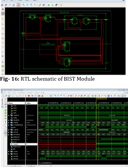
4.4.BIST module:
[image:6.595.323.562.130.302.2]The RTL Schematic of BIST is shown in fig-16. The pattern generated by LFSR is transmitted from transmitter and received in receiver FIFO. The transmitter FIFO is compared with the receiver FIFO after the reception of each word. The comparison starts after the delay of transmitter for sending the data and receiver for reception of the data. In this simulation, the first byte sent is “11111111” which matches in both FIFO; hence the test status bit B0 is set. Simulation of BIST module is shown in fig-17.
Fig- 16: RTL schematic of BIST Module
Fig- 17: Simulation result of BIST Module
[image:6.595.36.260.257.549.2]4.5. Synthesis Report:
Table-1: Timing summary
Timing summary Speed Grade: -4
Minimum period 7.851ns
(MaximumFrequency:12 7.372MHz)
Minimum input arrival
time before clock 8.452ns Maximum output
required time after clock 7.498ns
Total 7.851ns (3.678ns logic, 4.173ns route) (46.8% logic, 53.2% route)
Table -2: Device utilization summary
Table-3: Performance parameter comparison
5. CONCLUSIONS:
With the implementation of BIST, expensive tester requirements and testing procedures starting from circuit or logic level to field level testing are minimized. The LFSR replaces the function of the external tester features such as a test pattern generator by automatically generating pseudorandom patterns to give good fault coverage to the UART module.
Device utilization summary Selected Device : 3s50pq208-4
Number of Slices 41 out of 768 5%
Number of Slice Flip Flops 22 out of 768 2%
Number of 4 input LUTs 37 out of 1536 2%
Number of IOs 17
Number of bonded IOBs 15 out of 124 12% IOB Flip Flops 1 out of 124
13%
Number of GCLKs 1 out of 8 12%
Number of
Reference paper[6]
Reference paper[4]
Present simulation
Slices
(CLB)
38 out of 768 (4%)
513 out of 4656 (11%)
41 out of 768 (5%)
Slices (ff) 49 out of 1536 (3%)
626 out of 9312 (6%)
22 out of 768 (2%)
4 input LUTS
54 out of 1536 (3%)
819 out of 9312 (8%)
37 out of 1536 (2%)
Bonded IOBs
19 out of 96 (19%)
16 out of 96 (16%)
15 out of 124 (12%)
GCLKs 1 out of 4 (25%)
1 out of 24 (4%)
1 out of 8 (12%)
[image:6.595.326.567.361.636.2]© 2016, IRJET | Impact Factor value: 4.45 | ISO 9001:2008 Certified Journal | Page 343
Result of this project is compared with referencepaper [6] providing number of CLBs, LUTs, Bonded I/Os used by Spartan3 is 38, 54, 19 and simulation time 9.668ns. It indicates improvement in area from 8.667% to 6.334% and overall 2.33% area reduction. Simulation time (delay) is reduced from 9.668 ns to 7.498 ns overall 2.170 ns reduction in delay
6. REFERENCES:
[1] Naresh, Vatsalkumar and Vikaskumar Patel, “VHDL Implementation of UART with Status Register”, in the proceedings of International Conference on Communication Systems and Network Technologies, IEEE Computer Society, 11-13th May 2012, DOI: 10.1109/CSNT.2012.164, pp.750-754.
[2] Fang Yi-yuan and Chen Xue-jun, “Design and Simulation of UART Serial Communication Module Based on VHDL”, in the proceedings of 3rdInternational Workshop on Intelligent Systems and Applications (ISA), IEEE, May 2011, DOI: 10.1109/ISA.2011.5873448, pp.1-4.
[3] Dr. Garima Bandhawarkar Wakhle, Iti Aggarwal and Shweta Gaba, “Synthesis and Implementation of UART using VHDL Codes”, in the proceedings of International Symposium on Computer, Consumer and Control, IEEE June 2012, DOI: 10.1109/IS3C.2012.10.
[4] Parul Sharma and Ashutosh Gupta “Design, Implementation and Optimization of HighlyEfficient UART”
[5] ”A Review on Serial Communication by UART” Ms.Neha R. Laddha , Student and Prof. A. P. Thakare Head of the Department of Electronics and Telecommunication Sipna’s COET, A Amravati (MS) INDIA. Volume 3, Issue 1, January 2013 ISSN: 2277 128X International Journal of Advanced Research in Computer Science and Software Engineering. [6] Bibin M C, Premananda B S, “Implementation of
UART with BIST Technique in FPGA” International Journal of Inventive Engineering and Sciences (IJIES). ISSN: 2319– 9598, Volume-1, Issue-8, July 2013.
[7] Mohd Yamani Idna Idris, Mashkuri Yaacob and Zaidi Razak, “A VHDL Implementation of UART Design with BIST Capability”, in the proceedings of Malaysian Journal of Computer Science, June 2006, Vol. 19(1), pp. 73-86. Design and Implementation of UART with BIST Technique Department of P.G Studies VTU Belgaum-580018 Page 36