http://www.sciencepublishinggroup.com/j/ajee doi: 10.11648/j.ajee.20180604.11
ISSN: 2329-1648 (Print); ISSN: 2329-163X (Online)
Study of the Influence of the Content of a Potassium
Fluoride Layer on the Capacitance and Conductance of a
CIGS Thin-Film Solar Cell
Djimba Niane
1, 2, Ousmane Diagne
1, 2, Demba Diallo
1, 2, Gerome Sambou
1, 2, Moustapha Dieng
1, 21Physics Department, Faculty of Science and Technology, University Cheikh Anta Diop, Dakar, Senegal 2
Laboratory of Semiconductors and Solar Energy, University Cheikh Anta Diop, Dakar, Senegal
Email address:
To cite this article:
Djimba Niane, Ousmane Diagne, Demba Diallo, Gerome Sambou, Moustapha Dieng. Study of the Influence of the Content of a Potassium Fluoride Layer on the Capacitance and Conductance of a CIGS Thin-Film Solar Cell. American Journal of Energy Engineering.
Vol. 6, No. 4, 2018, pp. 38-43. doi: 10.11648/j.ajee.20180604.11
Received: October 27, 2018; Accepted: November 15, 2018; Published: December 20, 2018
Abstract:
In this paper, a study by simulation of the capacitance and conductance of carriers of a heterojunction composed of a layer of Zinc oxide (ZnO), a layer of cadmium sulphide (CdS) and a layer of CIGS under the influence of a potassium fluoride (KF) layer placed in the CIGS / CdS interface is made. The simulation done with the SCAPS-1D software. Measurements on the capacitance-tension, the conductance-tension, the capacitance-frequency and the conductance-frequency are taken. The capacitance-voltage measurement shows an increase in capacitance as a function of the voltage and a decrease in its module when the KF layer is present in the CdS / CIGS interface. The conductance-voltage measurement also shows an increase in the conductance as a function of the voltage and when the KF layer isn’t present. The capacitance-frequency measurement shows a constancy of capacitance for the low values of the frequency and a decrease for the large values of the frequency. While the conductance-frequency characteristic shows an increase in the conductance with the frequencies. The measurements conductance-frequency and capacitance-frequency show a decrease in their modules when the KF layer is put into the CdS / CIGS interface. Besides, the total capacitance and the total conductance of the solar cell are determined according to the thickness of the KF layer. The measures reveal aussi that the capacitance and the conductance decrease with the increase in the thickness of the KF layer. The decrease in capacitance is caused by a passivation of the interface states while that of the conductivity is caused by the increase of the resistivity of the CIGS layer.Keywords: Solar Cells, Thin-Film, CIGS, KF, Capacitance, Conductance, Simulation
1. Introduction
Because of its optimal direct band, its high absorption coefficient and its long-term stability, copper, indium and gallium diselenide-based solar cells called Cu (In, Ga) Se2 in particular have the best performance in second-generation solar cells [1]. This technology is very promising and its performance continues to increase with the use of alkalis such as NaF, KF, RbF and CsF in the elaboration of the absorber [2-5]. Despite these excellent results, the mechanism of distribution of interface states on performance is still debated in research [6]. Indeed, the electrical behavior and performance of CIGS thin-film solar cells is mainly influenced by the defects levels at the CdS / CIGS interface and in most of the depletion region [7]. There are several techniques to
study the distribution of the states of interfaces (defects) in CIGS thin films such as deep level transient spectroscopy (DLTS) [8, 9], photoluminescence, capacitance-voltage (C-V) measurements, conductance-voltage (G-V), drive level capacitance profiling (DLCP), or admittance spectroscopy (AS) [10, 11]. In this work, the capacitance and conductance of a thin film solar cell based on CIGS under the influence of the KF layer placed in the CdS / CIGS interface are studied using C-V measurements, G-V measurements and spectroscopy admittance.
2. Numerical Modelling
describe the functioning of the solar cell. In this work, the model used is the SCAPS-1D software. According to the presentation, SCAPS -1D (Solar Cell Capacitance Simulator in one Dimension) is a one-dimensional numerical simulation software, developed at the ELIS (Electronics and Information Systems) laboratory of the University of Gent, Belgium by M. Burgelman et al. [12, 13]. It is application software on Windows. It has been developed to simulate heterojunction and thin-film solar cells consisting of up to 7 layers.
The main functionality of SCAPS is to solve the one-dimensional semiconductor equations. In the bulk of the layers these equations are given by:
Ψ = − − + − +
(1)
− + = (2)
− + = (3)
Where:
(1)ε is the dielectric constant, (2)Ψ the electrostatic potential,
(3)n and p the concentration of the free carriers,
(4) and are the densities of the ionized acceptors and donors,
(5) and the current densities of electrons and holes, (6)!"#$ defect distributions,
(7)Un, Up the net recombination rates of electron and hole respectively,
(8)and G the generation rate.
The expressions of and are given by:
= −% &' (4)
= −% &' (5)
(1)( , ( are the carriers mobility ,
(2)*+ , *+ are the quasi-Fermi energies of the electrons and holes respectively.
Together with appropriate boundary conditions at the interfaces and contacts, this results in a system of coupled differential equations in (Ψ, n, p) or (Ψ, *+ , *+ ). SCAPS numerically calculates a steady state and a small signal solution of this system. Hereto, the structure is first discretized [14, 15].
The DC solution is given by partitioning the simulation domain into number of subdomains. Indeed, the differential equations are replaced by algebraic equations, in each subdomain. The classical method of three-point discretization is used in this software to solve the algebraic equations iteratively. Thus, we obtain a discrete Poisson's equation, by supposing that the electric field is constant in each subdomain. The discretization of continuity equations are obtained by using exponentially fitted finite difference scheme. The sets of variables used for the resolution are the normalized electrostatic potential qΨ/kT and the following functions of quasi-Fermi energies.
, = -. &' /0 − -.
1
/0 (6)
2 = -. &'
/0 − 1 (7)
Where, V is the applied bias and kT is the Boltzmann constant multiplied by the absolute temperature.
Here, the electrostatic potential is referenced to its value at the absorber contact and the quasi-Fermi energy are referenced to the equilibrium Fermi energy EF. The discrete continuity equations are linear in u and v. A nonlinear matrix system of 3N to 3N variable equations is obtained with N nodes:
45"67Ψ999:, ,9:, 2:; = 0 (8) 4="67Ψ999:, ,9:, 2:; = 0 (9) 4>"67Ψ999:, ,9:, 2:; = 0 (10)
Where 45"6 denotes the N- dimensional vector function with components, the discrete Poisson equation with N nodes and arguments, the variables 7Ψ9999:, ,? 999:, 2?999:;? , with i=1, 2…N. the Newton Raphson method is used to solve this total system of 3N equations separated into three subsystems of N variable N equations.
The time dependent semiconductor equations are discretized and considering the variables (Ψ, n, p), the equations are given by [14]:
45@7Ψ999:, 9:, :; = 0 (11) 4A@7Ψ999:, 9:, :; = − B (12)
4C@7Ψ999:, 9:, :; = − B (13)
The equation in the frequency domain is obtained by linearizing equations (11), (12) and (13) around the dc solution. The derivatives with respect to time are replaced by jω, where ω is the angular frequency of the ac-excitation. With the dc solution 4A@7Ψ9999:, 9: , : ; = 0 the first order Taylor expansion of the discrete continuity equations for electrons at node i is given by:
∑ +EF
5G H
/IJ ΨLK+ +AEFG M/ + +CNFG M/=−jωO? (14)
Where 7ΨP, M, M; are the small signal amplitudes of the potential, carrier concentrations at node i. After linearization of the Poisson equation and continuity equations, linear system of 3N equations with 3N variables are obtained. As the system is linear, the solution is found by finding the lower-upper decomposition of N x N matrix with 3x3 matrices as elements.
For node i, 3x3 matrix QB/ is given by :
R S T
+ΨF
5G
+ΨF
AG
+ΨF
G +EF
5G +EF
AG+ UVWB/
+EF CG +NF 5G +NF AG +NF
CG+ UVWB/X Y Z
[\ = ]? ΨLK
M/ M/
^ (16)
_O?=` ab 0 0 c
(17)
_O 0? for i<N and ab is the small signal amplitude of the applied bias. The ac system thus becomes:
Q[O _̃ (18) In order to avoid the numerical problem, equation (32) is scaled using the S (n x n) scaling matrix. The elements of scaling matrix is given by:
eB,/ WB/QB,/fJ (19)
The small signal amplitude g is calculated after obtaining the solution for potential and carrier concentrations. Thus, the capacitance and conductance can be calculated by using the following equation:
hVi j- kg (20)
lhVi mJno kg (21)
The structure studied consists of an n-type doped zinc oxide layer, an n-type doped CdS layer and the p-type doped CIGS absorbent layer. It is represented in figure 1. The KF layer is placed between the CIGS absorbing layer and the CdS buffer layer. The KF layer has a band gap of 1.5eV, its electronic affinity 4.14 eV and its dielectric constant 6.05 eV [16].
Figure 1. Structure of a heterojunction solar cell n-ZnO/n-CdS/p-CIGS.
The basic parameters of the four cell layers used in the simulation are shown in Table 1.
Table 1. The basic parameters of the different layers of the cell used in the simulation: (a) and (d) denote the acceptor and donor states respectively.
Layer properties CIGS KF CdS ZnO Al-ZnO
W (µm) 2,5 - 0,05 0,05 0,2
Eg (eV) 1,2 1,5 2,4 3,3 3,6
χ (eV) 4,5 4,17 4,2 4,45 4,45
⁄ 13,6 6,05 10 9 9
6hqofri 2,2. 10Ju 2,2. 10Ju 2,2. 10Ju 2,2. 10Ju 2,2. 10Ju
1hqofri 1,8. 10Jw 1,8. 10Jw 1,8. 10Jw 1,8. 10Jw 1,8. 10Jw
( hqo/yi 100 100 100 100 100
( hqo/yi 25 25 25 25 25
"z {|#hqofri 1. 10J} (a) 1. 10J~(a) 1. 10Ju(d) 1. 10Ju(d) 1. 10~(d)
3. Results and Discussions
3.1. Capacitance
Capacitance measurements are widely used techniques for studying the properties of a p-n junction. A variation dV of the bias voltage Vi causes a variation dW of the width of the space charge zone, and consequently a variation dQ per unit area given by:
•€ ‚••a (22)
With ε is the dielectric constant of the CIGS.
Thus the variation of the load dQ is proportional with the variation of tension. It results from it a behavior of the junction as being a condenser of differential capacity by unit area expressed as:
l "ƒ"1 ‚• (23)
Figure 2. Capacitance as a function of the voltage in the case where there is no KF and in the presence of KF.
The behavior of the C-V characteristic shows the proportionality of the capacitance as a function of the bias voltage. A small increase in capacitance for low voltage values (V <0.4) is noted; this phenomenon reflects the important shift of minority carriers at the junction. Whereas for large values of voltage (V> 0.4), capacitance increases exponentially; caused by a storage of minority carriers at the junction. On the other hand, the capacitance of the cell is more important in the case where the KF is not present at the hetero junction. This is explained by the increase in carrier flow that crosses the junction when the KF layer is present. As a result, a decrease in the stored charge results. In the following, the determination of the capacitance as a function of the frequency in the case where there is no KF and in the presence of KF is performed.
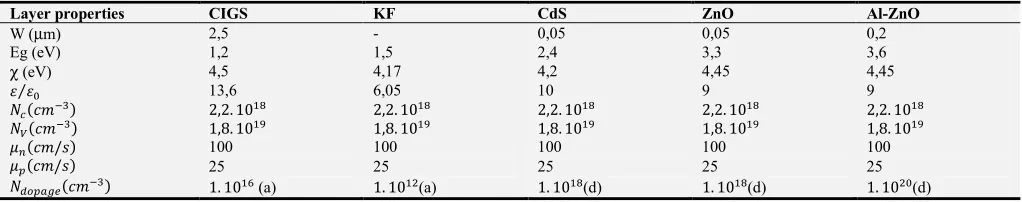
The capacitance-frequency characteristic without KF and with KF respectively, is shown in figure 4 and figure 5.
Figure 3. Capacitance-frequency characteristic without KF.
Figure 4. Capacitance-frequency characteristic with KF.
The observations made in Figure 4 and Figure 5 respectively show that the capacitance remains constant for low values of the frequency (f <106Hz) corresponding to the static regime. This means that the interface states can’t follow the AC signal and therefore can’t contribute much to the capacity. For high frequencies (f> 106Hz) corresponding to the dynamic frequency regime, the capacitance decreases asymptotically.
In addition, Figure 4 and Figure 5 respectively show a decrease in the capacitance module when the KF layer is put into the CIGS / CdS interface.
The effect of thickness of the KF layer on the total capacitance of the solar cell is represented in Figure 5.
Figure 5. The effect of thickness of the KF layer on the total capacitance of the solar cell.
this interface, it results in a massive crossing of the carriers in the space charge zone. In addition, as the KF layer increases the current density of the cell. Consequently, this results in a destocking of the free carriers at the junction.
3.2. Conductance
In a polarized P-N junction in the direct sense by a V voltage, conductance can be written from the expression of the J current density in the following way:
/0 (24)
With „-…†‡ˆ (25)
„ is a pre-factor named saturation current density.
The conductance-voltage characteristic for one cell with KF and another without KF is shown in Figure 6.
Figure 6. Conductance-voltage characteristic for one cell with KF and another without KF.
On the one hand, Figure shows that the conductance is constant for voltages less than 0.55V. While for the tensions superior to 0.55 V, the conductance increases exponentially. Indeed, for a given voltage; the Fermi level sets the occupation of trap levels. Thus, a variation in the voltage accentuates the response of the traps to the signal, resulting in an increase in the conductance. On the other hand, a decrease in the peak of the conductance is noted when the KF layer is present in the cell.
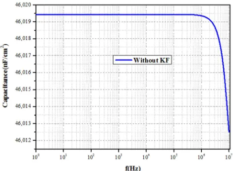
Figure 7 represent the conductance-frequency characteristic for one cell with KF and another without KF.
It appears from this figure that for frequencies below 105 Hz corresponding to the static regime, there is no variation of the conductance as a function of its frequencies for the different samples. This shows that for its frequencies, each component of the alternating current of the conductivity is negligible. It is as well as that the conductance is more important for the cell without KF than with the cell in the presence of KF in this frequency range. The analysis of the figure also shows, on the one hand, for frequencies greater than 106 Hz corresponding to the dynamic frequency regime that the conductance increases
exponentially with its frequencies. And on the other hand that the maximum value of the conductivity is reached by the cell in the presence of KF. This great value is explained by the fact that for high frequencies the addition of KF contributes to a much wider distribution of interface states. Consequently, it results a greater response from the AC signal that increases conductance.
Figure 7. Conductance-frequency characteristic for one cell with KF and another without KF.
The evolution of the conductance for a given frequency as a function of the thickness of the KF layer is represented in Figure 8.
Figure 8. Conductance for a given frequency as a function of the thickness of the KF layer.
These fluctuations in the conductance can be caused by a distribution of energy spread interfaces states.
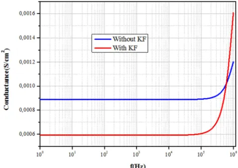
The total conductance as a function of the thickness of the KF layer is shown in Figure 9.
Figure 9. Total conductance as a function of the thickness of the KF layer.
Figure 9 shows that the conductance decreases to a minimum value of about 5nm, then it slightly increases to a peak noted around 10nm. This peak widens to a thickness of around 25 nm and finally a decrease follows. The presence of KF accentuates the hole density at the CIGS / CdS interface. The KF layer allows also a widening of the gap energy. This results in a reduction of the carrier mobility at the junction. Consequently, the resistance of the material increases. In addition, the inhomogeneous profile of the conductance is attributed to the inhomogeneity of the CIGS layer.
4. Conclusion
The capacitance and conductance constitute electric parameters very important of the solar cell. The study of the capacitance and conductance of CIGS-based solar cells is strongly influenced by the distribution of interface defects. In this work, the capacitance and the conductance under the influence of the thickness of a KF layer are studied. The results showed on the one hand a decrease in the capacitance due to the crossing of the carriers. And on the other hand a decrease in the conductance caused by an increase in the resistivity of the CIGS material when the KF content is too great.
References
[1] Philip Jackson , Roland Wuerz, Dimitrios Hariskos, Erwin Lotter, Wolfram Witte, and Michael Powalla, “Effects of heavy alkali elements in Cu (In, Ga) Se2solar cells with efficiencies up to 22.6%”Phys. Status Solidi RRL 10, No. 8, 583–586 (2016).
[2] M. A. Contreras, B. Egaas, P. Dippo, J. Webb, J. Granata, K. Ramanathan, S. Asher, A. Swartzlander, and R. Noufi, “On the role of Na and modifi-cations to Cu (In, Ga) Se2 absorber
materials using thin-MF (M = Na, K, Cs) precursor layers,” in Proc. 26th IEEE Photovoltaic Spec. Conf., 1997, pp. 359–362. [3] R. Wuerz, A. Eicke, F. Kessler, S. Paetel, S. Efimenko, and C. Schlegel, “CIGS thin-film solar cells and modules on enamelled steel substrates,” Sol. Energy Mater. Sol. Cells, vol. 100, May 2012, pp: 132–137.
[4] A. Chirila, P. Reinhard, F. Pianezzi, P. Bloesch, A. R. Uhl, C. Fella, L. Kranz, D. Keller, C. Gretener, H. Hagendorfer, D. Jaeger, R. Erni, S. Nishiwaki, S. Buecheler, and A. N. Tiwari, “Potassium-induced surface modification of cu (in, ga)se2 thin films for high-efficiency solar cells,” Nature Materials, vol. advance online publication, vol (12)pp 1-5 Nov. 2013. [5] P. Jackson, D. Hariskos, R. Wuerz, O. Kiowski, A. Bauer, T.
M. Friedlmeier, and M. Powalla, “Properties of Cu (In, Ga)Se2 solar cells with new record efficiencies up to 21.7%,” Phys. Status Solidi RRL – Rapid Res. Lett., vol. 9, no. 1, Jan. 2015, pp. 28–31.
[6] K. Decock, S. Khelifi, S. Buecheler, F. Pianezzi, A. N. Tiwari, M. Burgelman, Defect distributions in thin film solar cells deduced from admittance measurements under different bias voltages, Journal of Applied Physics, 110 (2011) 063722. [7] Habibe BAYHAN, A. Sertap KAVASOGLU, “Admittance and
Impedance Spectroscopy on Cu (In, Ga)Se2 Solar Cells” Turk J. Physic, Vol 27 (2003) , 529-535.
[8] R. N. Bhattacharya, A. Balcyoglu and K. Ramanathan, Thin Solid Films., 384, (2001), 65.
[9] M. Igalson, M. Bodegard, L. Stolt and A. Jasenek, Thin Solid Films., 431-432, (2003), 153.
[10] D. Schroder, Semiconductor Material and Device Characterization, 2nd ed. (Wiley & Sons, Toronto, 1998). [11] J. T. Heath, J. D. Cohen, and W. N. Shafarman, J. Appl. Phys.
95, 1000 (2004).
[12] M. Burgelman, P. Nollet, S. Degrave, “Modelling polycrystalline semiconductor solar cells”, Thin Solid Films 361/362 (2000) pp.527–532.
[13] M. Burgelman, K. Decock, S. Khelifi and A. Abass, “Advanced electrical simulation of thin film solar cells”, Thin Solid Films, 535 (2013) 296-301.
[14] A. Niemegeers, S. Gillis, M. Burgelman, A user program for realistic simulation of polycrystalline heterojunction solar cells: SCAPS-1D, Proceedings of the 2nd World Conference on Photovoltaic Energy Conversion, Wien, 1998, pp. 672-675. [15] S. Selberherr, Analysis and Simulation of Semiconductor
Devices, Springer Verlag, Wien-New York, 1984.