Jeyalakshmi M. et al., IJSRR 2019, 8(2), 233-250
IJSRR, 8(2) April. – June., 2019 Page 233
Research article Available online www.ijsrr.org
ISSN: 2279–0543
International Journal of Scientific Research and Reviews
Optimization of Code Converters Using Ms Gate in Quantum Dot
Cellular Automata
Jeyalakshmi M.
*and Santhi M.
*Department of Electronic and Communication Engineering, SSM Institute of Engineering and Technology, Dindigul, India E-mail:[email protected]
Department of Electronic and Communication Engineering,Saranathan College of Engineering, Tiruchirappalli., IndiaE-mail: [email protected]
ABSTRACT
Quantum Dot Cellular Automata (QCA), the most efficient Technology at nanoscale level in quantum electronics has replaced the CMOS technology due to very high Integration density, low power consumption, high speed and low circuit area. This work proposes a novel binary to grey and grey to binary code converters using an optimized MS gate .The proposed low complexity optimized MS gate can overcome the Feynman gate with reduced number of quantum cells thereby reducing the area and power consumption. The proposed MS gate requires only 31number of total cells and total area of 37,772nm2 whereas the Feynman gate in previous work requires 54 number of total cells 38,880 nm2 areas. The proposed design was compared with the previous work and it was analyzed that about 42% optimization has been achieved in terms of number of QCA cells and area respectively when compared to previous results. Code Converters based on MS gate can be used to realize nanotechnology based architecture which will be used for nano-communication. The efficiency of the nano circuits has been achieved through the proposed work. QCA Designer-2.0.3 tools are used for evaluating the functionality of the digital circuits.
KEYWORDS:
Quantum Dot Cellular Automata, Optimized MS gate, Code converters, QCA designer tool.*Corresponding author:
Jeyalakshmi M.
Assistant Professor,
Department of Electronic and Communication Engineering, SSM Institute of Engineering and Technology,
Dindigul, India
Jeyalakshmi M. et al., IJSRR 2019, 8(2), 233-250
IJSRR, 8(2) April. – June., 2019 Page 234
INTRODUCTION
CMOS Technology was one of the most prominent technologies for applications like Microprocessors, Static RAM, Microcontrollers and application specific integrated circuits (ASICs) in the past decades. The features of CMOS technology include noise immunity, static low power consumption, very high operating speeds and efficient usage of energy.
However CMOS technology have practical limitations when subject to nano level scaling. Recently, the most emerging technology at nano scale called Quantum Dot Cellular Automata(QCA). High-performance, higher densities, higher operating speed ,low power consumption are the most important features of QCA technology. Here, the method of computation and information transformation in QCA differs from CMOS technology. All digital circuits like combinational and sequential circuits designed in CMOS technology have been replaced by this new efficient switching technology. The information is transferred by processing in wire.
Exclusive –OR operation are fundamental circuits for analyzing most of the digital system. Several Exclusive –OR designs in QCA have been proposed2 and a performance comparison was presented .Better Exclusive –OR gate depends on minimizing the number of cells and thereby reducing the delay. A wide variety of (often complex) techniques have been used for EX-OR circuits design. Conventional EX-OR circuits frequently requires many cells1 which are relatively difficult to realize in QCA technology. This work presents a new binary to gray and gray to binary code converters design that is optimized by using proposed Novel MS gate in QCA technology.
II.LITERATURE SURVEY
Plenty of works have already been reported by the researchers on QCA-based reversible logic circuit design 3. A number of those are outlined in this paper through 3,5,6,7,8,9,10. In 5, two novel reversible gates termed as QCA1 and QCA2 are proposed and their QCA implementation is described. Those circuits are verified using Fred kin gate and Toffoli gate by considering the circuit density and clock delay as well. In6, the reversible computing capabilities of QCA circuit are illustrated by using Landaulet and Bennett clocking mechanism and also the thermodynamic activities of QCA circuit are investigated against operational speed and heat energy dissipation.
Jeyalakshmi M. et al., IJSRR 2019, 8(2), 233-250
IJSRR, 8(2) April. – June., 2019 Page 235
The design is compared with previous QCA Feynman gate designs. In existing work, reversible 4-bit binary to gray code converters has been designed using QCA technology. The number of cells, cell area, total area and delay due to clock cycles has been very high and so energy as well as power consumption of previous code converters was very high. Code converters design has not been widely designed with reduced number of cells by QCA designers. QCA code converters design in 1, suggests the importance of design but not with reduced number of cells. Complex designs generally incur long delays in QCA, so a simple structure is a good choice for the starting point. The proposed work investigates the QCA based design of reversible binary to grey and grey to binary code converter and its implementation.
The literature survey follows as:
1) QCA-based design of MS gate.
2) Proposed MS gate are used for the first time to achieve the design of reversible binary to grey and grey to binary code converter circuits.
3) The analysis of simulation results of proposed work with theoretical aspects shows the improvement in the efficiency of the circuits.
This paper is organized as follows: In section III, fundamentals of QCA and design approaches are presented. Section IV describes the design and Implementation of proposed Novel MS gate design and code converters based on proposed gate. Simulations results and comparisons are presented in section V. In Section VI conclusions are presented.
III.
QCA CELL
1.
QCA basics
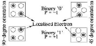
The basic computing element of QCA is a cell. Cells are composed of four quantum-dots. The quantum dots are sited at corners of the cell 1. Among four, two quantum dots are occupied by free electron. Each quantum dot is a semiconductor nanostructure that exhibits quantum mechanical properties in its size. Four dots form a QCA cell with one occupy opposite corner (diagonal) quantum-dots because Coulomb repulsion is less compared to the scenario when they are in adjacent quantum dots. Dots are coupled by tunnel junctions. The cellular automata (CA) notion is due to the fact that the state of a given cell at a particular time depends on the state of its neighbors during the previous clock cycle.
The Boolean logic functions used to design combinational circuits can be implemented by arrays of cells representing binary information, the so-called quantum-dot cellular automata (QCA) 1.
Jeyalakshmi M. et al., IJSRR 2019, 8(2), 233-250
IJSRR, 8(2) April. – June., 2019 Page 236
Fig 1:Qca Cell
2.Normal cells and rotated cells
Two arrangement of cells are normal cell of 90°phase and rotated cells of ‘45°’phase which was shown in below fig 2.Normal cells and rotated cells transmit the information which was perpendicular to each other.
Fig 2 : Normal Cell And Rotated Cell
3.QCA wire
QCA wire can be constructed by grouping cells together either horizontally or vertically12 .Binary wire classification can be done by grouping normal cells and another by grouping rotated cells which was shown in below fig 3.Normal cells transmit the information given at the input.
Fig 3: QCA 90 Wire And QCA 45 Wir
4. Basic QCA element and logic gates
• QCA Majority voter
The three important primitive logic gates in QCA are the 3-input majority gate, AND
gate, OR gate, inverter and wire11. The basic element in QCA is the 3-input majority gate which has cells on the top, at the left and at the bottom. These cells function as connection cells in the input. As summing the Coulomb forces of all the electrons. The middle cell adjusts to the majority of adjustments of the input connection cells. Finally, the output cell adjusts to the middle cell and the resulting state of the majority vote can be obtained from the output cell as shown in fig 4.
Jeyalakshmi M. et al., IJSRR 2019, 8(2), 233-250
IJSRR, 8(2) April. – June., 2019 Page 237 The majority function, M(A, B,C) with two inputs A, B and a control input C shown
above in fig is given by equation
M (A, B, C) = AB+ BC + AC (1)
• AND gate
The two input AND gate can be realized by setting control input C=0 to indicate
polarization P=-1 in order to propagate binary value Logic”0”.So the output function becomes
M(A,B,0) = AB which was shown in below fig 5
Fig 5: QCA AND Gate
• OR gate
The two input OR gate can be realized by setting control input C=1 to indicate
polarization P=+1 in order to propagate binary value Logic”1”. So the output function becomes
as in equation given below M(A, B,1) = A+B……(2) which was shown in below fig 6.
Fig 6 : QCA OR GATE
• QCA crossover
In Quantum Dot Cellular Automata, there are two types of crossovers. Coplanar
crossover 12, which is achieved by using two different quantum dot orientations (one at 45
degrees to theother) i.e., array of normal cells and rotated cells passes perpendicularly to each
other. This type propagates polarization without change; the other reverses polarization from one
adjacent cell to the next .The interaction between two different wires produces no net
polarization change in either wire. Therefore the signals passed over these wires are preserved.
But since this design has some problems such as crosstalk, alternative methods should be utilized for solving such problems. In multilayer crossovers, signals can be effectively crossed
between different layersi.e., more than one layer can be effectively used to transmit the signals.
The Coplanar crossover and multilayer crossovers are shown in fig 7(a), 7(b).
Jeyalakshmi M. et al., IJSRR 2019, 8(2), 233-250
IJSRR, 8(2) April. – June., 2019 Page 238 IV
. REVERSIBLE BINARY TO GREY AND GREY TO BINARY CODE
CONVERTER USING MS GATE
1. MS Gate
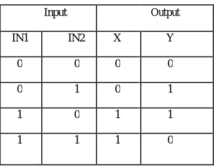
MS is a 2x2 reversible gate 9,10,11 having input (a ,b)mapped to unique output (x, y) as x=a and y= AB, respectively .The truth table of MS gate is shown in Table 1.
Table 1: Truth table of reversible MS gate
Input Output
IN1 IN2 X Y
0 0 0 0
0 1 0 1
1 0 1 1
1 1 1 0
The logic expression for MS gate in QCA majority gate can be derived from the truth table and its equations are
X=IN1
(3)
Y=M((IN1,IN2,-1),M(IN1,IN2,1),-1)
(4)
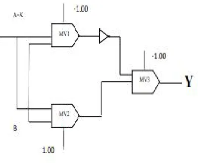
2. Proposed MS Gate
The block diagram of proposed MS gate was given in fig 7.It shows that only two inputs are required for proposed MS gate .The inputs given to the circuit are IN1 and IN2 and its corresponding output are X and Y.
IN1
x
MS gate
IN2 y
Fig 8:Block Diagram of MS gate
Jeyalakshmi M. et al., IJSRR 2019, 8(2), 233-250
IJSRR, 8(2) April. – June., 2019 Page 239
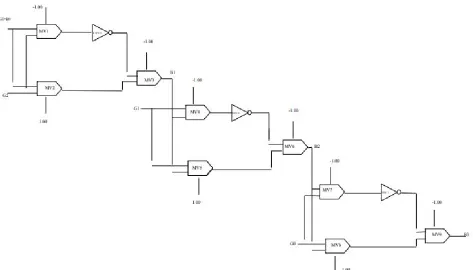
Fig 9: Schematic Diagram of Proposed MS gate Fig 10: QCA Layout of MS GATE
3.REVERSIBLE BINARY TO GREY CODE CONVERTER USING
MS-GATE
Let B3, B2,B1,B0 are the three bits of a binary code and G3,G2,G1, G0 are the corresponding three bits of the grey code. In grey code, the consecutive valuations vary in single variable only . The truth table of 4-bit binary to grey code conversion is shown in Table 2. From Table 2, it can be seen that the output G2 is same as input B2. The output G1 is XOR-ed value of inputs B1 and B2 whereas the output G0 is XOR-ed value of inputs B0 and B1 .
Table 2: Truth table of reversible 4-bit binary to gray code converter using MS-Gate
INPUT BINARY OUTPUT GRAY
CODE CODE
B3 B2 B1 B0 G3 G2 G1 G0
0 0 0 0 0 0 0 0
0 0 0 1 0 0 0 1
0 0 1 0 0 0 1 1
0 0 1 1 0 0 1 0
0 1 0 0 0 1 1 0
0 1 0 1 0 1 1 1
0 1 1 0 0 1 0 1
0 1 1 1 0 1 0 0
1 0 0 0 1 1 0 0
1 0 0 1 1 1 0 1
1 0 1 0 1 1 1 1
1 0 1 1 1 1 1 0
1 1 0 0 1 0 1 0
1 1 0 1 1 0 1 1
1 1 1 0 1 0 0 1
1 1 1 1 1 0 0 0
Thus, using truth Table 2 the logic expression of 3-bit binary to grey code converter can be written as equations given below
G0=B0 (5)
G1=B0 ^B1 (6)
G2=B1 ^B2 (7)
Jeyalakshmi M. et al., IJSRR 2019, 8(2), 233-250
IJSRR, 8(2) April. – June., 2019 Page 240
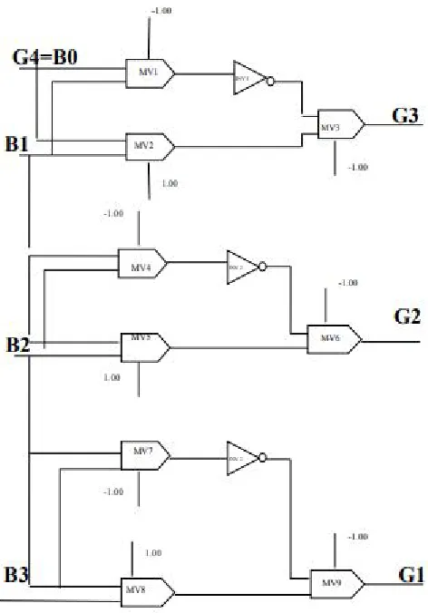
The QCA schematic diagram for Binary to Gray Code Converter was shown in figure 10 .In QCA schematic diagram of binary to gray code converter as shown in fig 10,let B3, B2,B1,B0 are the four bits of a binary code and G3,G2,G1, G0 are the corresponding four bits of the gray code. In grey code, the consecutive valuations vary in single variable only.
From schematic, it can be seen that the output G4 is same as input B0. The input B0 is xor-ed with B1 to produce the output G3. Then input B1 is xor-ed with B2 to produce the output G2. Then input B2 is xor-ed with B3 to produce the output G1.The information flow in QCA is a very important thing. In QCA circuit, the information flow in the adjacent cells, by controlling the polarization reactions and effects of adjacent cells. Therefore it is required to hold the polarization of first cell fixed and lower the potential barrier of its adjacent cell in order to let the electrons of adjacent cell relocate
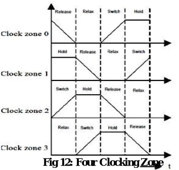
This processing should occur repeatedly throughout the cell to pass the information. QCA Clocking mechanism consists of four clocking zones for the proper functioning of it and is represented as shown in the fig. (2). QCA circuits require clock not only to synchronize & control information flow but also to provide the power to run the circuit since there is no external source for powering cells (serial adders, shifters).With the use of four phases clocking scheme in controlling cells, QCA process and forwards information within cells as shown in fig 11.
Jeyalakshmi M. et al., IJSRR 2019, 8(2), 233-250
IJSRR, 8(2) April. – June., 2019 Page 241
Fig 12: Four Clocking Zone
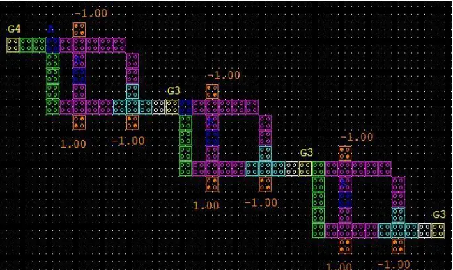
The QCA layout of binary to gray code converter using MS Gate was shown in fig 12.
Jeyalakshmi M. et al., IJSRR 2019, 8(2), 233-250
IJSRR, 8(2) April. – June., 2019 Page 242
The corresponding QCA majority gate expression for Binary to Gray Code Converter using MS Gate can be drawn as equations given below
To produce Grey code only three XOR operations are required. Thus, using the unique feature of reversible MS gate , the 4-bit grey to binary code converter can easily be realized .The corresponding schematic and layout of proposed MS-based reversible 4-bit binary to grey code converter circuit in QCA is expressed in fig 10 and 12,respectively.
G0=B0 (9)
G1= M((B0,B1,-1),M(B0,B1,1),-1) (10)
G2= M((B1,B2,-1),M(B1,B2,1),-1) ) (11)
G3= M((B2,B3,-1),M(B2,B3,1),-1) ) (12)
4. REVERSIBLE GRAY TO BINARY CODE CONVERTER USING
MS-GATE
The input gray code is a non-weighted code. The consecutive gray code differs in one bit position .It is a unit distance code. It is also referred as cyclic code. Let G3, G2, G1, G0 are the four bits of a grey code and B3,B2,B1, B0 are the corresponding three bits of the binary code. The truth table of 4-bit grey to binary code conversion is shown in Table 3.
From the table, it can be seen that the output B2 is same as input G2. The output B1 is XOR-ed value of inputs B0,G1 whereas the output B2 is XOR-ed value of inputs B1, and G2 and so on and its QCA schematic was shown in fig 13.
Jeyalakshmi M. et al., IJSRR 2019, 8(2), 233-250
IJSRR, 8(2) April. – June., 2019 Page 243
The QCA layout for the proposed of Gray to Binary Code Converter is shown in fig 14
Jeyalakshmi M. et al., IJSRR 2019, 8(2), 233-250
IJSRR, 8(2) April. – June., 2019 Page 244
Table 3: Truth table of reversible 4-bit grey to binary code converter circuit using MS Gate
The corresponding QCA majority gate expression for Reversible Gray to Binary Code Converter using MS Gate can be drawn as equations given below
B0=G0 (13)
B1=B0 ^G1) (14)
B2=B1 ^G2) (15)
B3=B2 ^G3) (16)
The corresponding QCA majority gate expression can be drawn as equations given below B0=G0 (17)
B1= M((B0,G1,-1),M(B0,G1,1),-1) ) (18)
B2= M((B1,G2,-1),M(B1,G2,1),-1) ) (19)
Jeyalakshmi M. et al., IJSRR 2019, 8(2), 233-250
IJSRR, 8(2) April. – June., 2019 Page 245
V. RESULT AND DISCUSSIONS
Fig 15 shows the simulation outcome of proposed QCA-based reversible MS gate. The output is investigated for the proposed QCA-based reversible MS gate as shown in Table 1. The functional efficiency of the design was compared with previous Feynman gate. The proposed design is found to have reduced number of cells and better efficiency.
Fig 16: Simulation Output of Proposed Ms Gate
Here when the input IN1 = 0, IN2 = 0, then the output is X= 0 and Y=0 respectively. When the input IN1 = 0,IN2=1, then the output is X= 0 and Y=1 respectively and so on. The output X and Y appears after first clock pulse.. C0, C1, C2, and C3 represent the clock zone 0, clock zone 1, clock zone 2, and clock zone 3, respectively. The simulation output of proposed reversible MS gate is shown in fig 12.The simulation output of proposed reversible binary to grey code converter circuit is shown in fig 16.
Fig17: Simulation Output Of Proposed Binary To Gray Code Converter Using Ms Gate
Jeyalakshmi M. et al., IJSRR 2019, 8(2), 233-250
IJSRR, 8(2) April. – June., 2019 Page 246
Fig 18: Simulation Output of Proposed Binary To Gray Code Converter Using Ms Gate
Jeyalakshmi M. et al., IJSRR 2019, 8(2), 233-250
IJSRR, 8(2) April. – June., 2019 Page 247
Fig 19: Simulation Output of Proposed Gray To Binary Code Converter Using Ms Gate.
The outcome of proposed Gray to Binary Code Converter using MS Gate is verified with the theoretical values as in Table 3. It can be seen from fig 14 that when the binary input G3= 0, G2= 0, and G1 = 0,G0=0 then the grey code output with garbage value as B3= 0, B2 = 0, B1=0,B0=0 respectively. When the binary input G3= 0, G2= 0, and G1 = 0,G0=1 then the grey code output with garbage value as B3= 0, B2 = 0, B1=0,B0=1 respectively. Therefore, the circuit designed works proficiently. The output of G2, G1, and G0 appears after first clock pulse. C0, C1, C2, and C3 represent the CLOCK zone 0, clock zone 1, clock zone 2, and clock zone 3, respectively.
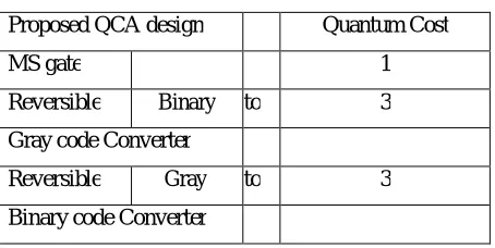
The quantum cost for the proposed design has been measured and it was found that For all 2x2 reversible gates, the quantum cost has measured as unity and for all reversible NOT gates (1x1 reversible gates) the quantum cost has measured as zero.
Table 4: Quantum Cost of Proposed work
Proposed QCA design Quantum Cost
MS gate 1
Reversible Binary to 3 Gray code Converter
Reversible Gray to 3 Binary code Converter
Jeyalakshmi M. et al., IJSRR 2019, 8(2), 233-250
IJSRR, 8(2) April. – June., 2019 Page 248
quantum cost 3 as shown in Table 4. The Proposed design characteristics was analyzed and was shown in Table 5
Table 5: Proposed design characteristics
Proposed QCA design Number of MV gate Number of QCA cell Total Area[nm2] Reversible Binary to
gray code converter
9 102 81,674
Reversible gray to Binary code converter
9 87 93,782
In the proposed work, the number of QCA cells used for designing MS gate is less compared to the previous Feymann gate. Also based on Proposed MS gate, the reversible Binary to Gray code converter and Gray to binary code converter using MS Gate designed requires less number of QCA cells than the previous work which was specified in the fig 15.
Fig 20 : Comparison Chart For Proposed WorkBased On Number Of Qca Cells.
Jeyalakshmi M. et al., IJSRR 2019, 8(2), 233-250
IJSRR, 8(2) April. – June., 2019 Page 249
In the proposed work, the total area used for designing MS gate is less compared to the previous Feymann gate. Also based on Proposed MS gate, the reversible Binary to Gray code converter and Gray to binary code converter using MS Gate designed requires less area than the previous work which was specified in the fig 16.
Fig 21 : Comparison Chart for Proposed workbased on number of qca cells.
VI CONCLUSION
The most critical issue in reversible computing circuit is to design a circuit at low power consumption in nanometer scale. For the first time, the reversible binary to grey and grey to binary code converter is designed based on QCA using MS gate. Both the proposed reversible binary to grey and grey to binary code converter circuits using MS Gate have quantum cost as 3.
The proposed circuit required only 32,160nm2 areas, 3 MVs, 31 cells, 1 inverter and 4 clocking
zones. The reversible binary to grey circuit required only 81,674 nm2 areas, 9 MVs, 3 inverters,102 cells, and 4 clocking zones whereas the reversible grey to binary circuit required only 93,782 nm2 areas, 9 MVs, 3 inverters, 87 cells, and 4 clocking zones. Therefore the efficiency of proposed design is better compared to the previous work so that it can be employed to realize the reversible computing nanoarchitecture in computer communication with low power consumption.
REFERENCES
Jeyalakshmi M. et al., IJSRR 2019, 8(2), 233-250
IJSRR, 8(2) April. – June., 2019 Page 250
2. Jadav Chandra Das & Debash is De. Reversible Binary to Grey and Grey to Binary Code Converter using QCA. IETE Journal of research 2015; 61(3).
3. K. Das, and D. De. Characterization, test and logic synthesis of novel conservative & reversible logic gates for QCA. Int. J. Nanosci, 2010; 9(3); 201_14
4. J. Huang, X. Ma, and F. Lombardi. Energy analysis of QCA circuits for reversible computing. in Proceedings of the Sixth IEEE Conference on Nanotechnology, Cincinnati, heartland, Jun. 17_20, 2006; 39_42.
5. X. Ma, J. Huang, C. Metra, and F. Lombardi. Testing reversible 1D arrays of molecular QCA. in Proceedings of the IEEE International Symposium on Defect and Fault Tolerance in VLSI Systems (DFT), Arlington; VA, 2006;71_9.
6. K. Das, and D. De. Novel approach to design a testable conservative logic gate for QCA implementation. in Proceedings of the 2nd International Conference on Advance Computing (IACC), Patiala; 2010; 82_7.
7. H. Thapliyal, and N. Ranganathan. Reversible logic-based concurrently testable latches for molecular QCA. IEEE Trans. Nanotechnol 2010; 9(1): 62_9,
8. N. A. Shah, F. A. Khanday, and J. Iqbal. Quantum-dot cellular automata (QCA) design of multi-function reversible logic gate. Int. J. Commun. Inf. Sci. Manag. Eng; 2012; 2(4): 8_18,.
9. H. Thapliyal, and N. Ranganathan. Concurrently testable FPGA design for molecular QCA using conservative reversible logic gate. in Proceedings of the IEEE International Symposium on Circuits and Systems, Taipei, 2009; 1815_8.
10.C. Lent, and P. Tougaw. A device architecture for computing with quantum dots. Proc IEEE 1997; 85(4): 541_57.
11. J. C. Das, and D. De. Quantum dot cellular automata based cipher text design for nano communication. in Proceedings of the International Conference on Raddar, Communication and Computing, Tiruvannamalai, 2012; 343_8.