Supreme Boost Control of Buck-Boost Voltage Source Converter with
X-Shape Diode-Capacitor Network
Sourabh R. Kurane¹, Ramchandra P. Hasabe²
1,2
Department of Electrical Engg., Walchand College Engg. Sangli
Abstract—Maximum Boost Control of Buck-Boost Voltage Source Inverter with X-Shape
Diode-Capacitor Network achieves high voltage gain by introducing a cross capacitor based high step up dc-dc circuit between the dc source and inverter circuit. For this unique circuitry, various pulse width modulation techniques are developed. In order to maximize the voltage, gain and reduced voltage stress on switches this paper proposed new PWM strategy. It regulates the average value of intermediate dc-link voltage in one switching time period (Ts) the same as the instantaneous maximum
value of three-phase line voltage by controlling the front boost circuit.The operating principle and closed-loop controller design are analyzed and verified by simulation and real time simulator OPAL-RT which shows real time result as physical counterpart would. Compared with existing PWM strategies, the new control strategy demonstrates less power device requirement and higher efficiency in high voltage gain applications. It is a more competitive method for range dc/ac voltage regulation in renewable energy applications. Furthermore, with new control strategy, the dc-side inductor current and capacitor voltage contains six-time line-frequency ripples. To overcome the undesired influence of low frequency ripples, it is also suitable for 400–800 Hz medium frequency aircraft and vessel power supply system.
Index Terms- Dc/ac conversion, voltage gain, high efficiency, minimum switching frequency, modulation strategy, Closed-loop control.
I.INTRODUCTION
The efficiency and environmental benefits of emerging solar and fuel cell technology, the distributed generation systems based on the renewable energy sources have rapidly developed in recent years. In photovoltaic (PV) systems, it is difficult to realize a series connection of the PV cells without incurring a shadow effect. Fuel cells and lightweight battery power supply systems are promising in future hybrid electric vehicle, more-electric aircraft and vessel. However, characteristic of these dc sources is low voltage supply with wide range voltage drop. Power electronic interface has to regulate the amplitude and frequency to obtain required high ac utility voltage. These applications raise stringent requirements for power converters such as low cost, high efficiency and wide range voltage buck–boost regulation ability.
International Journal of Modern Trends in Engineering and Research (IJMTER)
Volume 06, Issue 05, [May– 2019] ISSN (Online):2349–9745; ISSN (Print):2393-8161In view of additional power conversion stage increasing cost and lowering efficiency, a family of Z-source inverter [3] - [5] introduces a unique impedance network between the dc source and the inverter bridge. It achieves the desired output voltage that is larger than the available dc source voltage by adopting shoot-through (ST) operation mode. Z-source inverter provides a potential cheap and single-stage power conversion. However, the ST state limits the modulation index and accompanies large ST current.
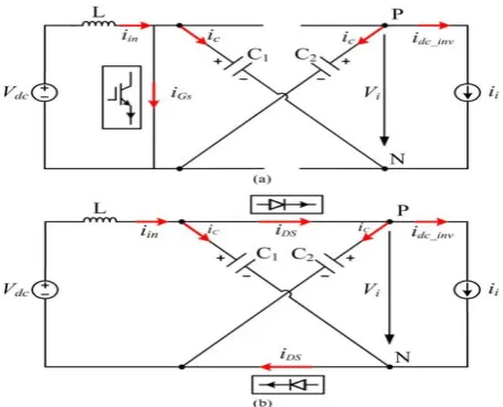
Although both of them can boost output voltage to any desired value without upper limitation in theory, the degradation of efficiency and increasing requirement of switching devices are prominent under high voltage gain. Existing proposed diode-assisted buck–boost VSI and related modulation strategy. The main circuit is shown in Fig. 1. It extends voltage gain and avoids extreme boost duty ratio by introducing a switch-capacitor based high step-up dc–dc circuit between the dc source and inverter bridge. The diodes are naturally conducting to perform capacitive charging in parallel and discharging in series to achieve high voltage gain. In view of chopped intermediate dc-link voltage, the front boost circuit and inverter bridge needs coordinate control. The existing typical modulation strategy in just utilizes intermediate dc-link voltage for ac output in the duration when the two capacitors are connected in series.
The diode assisted buck–boost VSI and related modulation strategy extends voltage gain and avoids extreme boost duty ratio by introducing a switch-capacitor based high step-up dc–dc circuit between the dc source and inverter bridge. The diodes are naturally conducting to perform capacitive charging in parallel and discharging in series to achieve high voltage gain buck -boost voltage source inverters with a unique X-shape diode-capacitor network inserted between inverter circuitry and dc source for producing a large voltage boost gain. Comparing with other voltage buck-boost techniques [1].
In order to achieve the increased efficiency as well as to maximize the voltage gain, this novel modulation strategy used. It regulates the average value of intermediate dc-link voltage in one switching time period Ts the same as the instantaneous maximum value of three-phase line voltage by controlling the front boost circuit. Then, the equivalent switching frequency of power devices in the inverter bridge can be reduced to 1/3fs (fs = 1/Ts). Compared with the existing modulation strategies, new proposed maximum boost control strategy contributes to less switching device requirement and higher efficiency in high voltage gain applications.
II.BLOCK DIAGRAM OF TOPOLOGY
International Journal of Modern Trends in Engineering and Research (IJMTER)
Volume 06, Issue 05, [May– 2019] ISSN (Online):2349–9745; ISSN (Print):2393-8161Fig.2 Block diagram of proposed topology
III. PROPOSED CIRCUIT DIAGRAM AND OPERATION
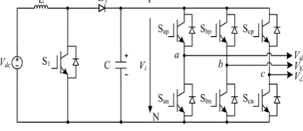
The circuit diagram voltage source inverter with X-shaped diode capacitor network circuit is shown in figure 3. The circuit comprises of X-shape diode capacitor network with voltage source inverter.
Fig. 3 Voltage source inverter with X-shaped diode capacitor network
International Journal of Modern Trends in Engineering and Research (IJMTER)
Volume 06, Issue 05, [May– 2019] ISSN (Online):2349–9745; ISSN (Print):2393-8161When S is turned off, the energy accumulated in the inductor is transferred to capacitors and both capacitors are connected in parallel to supply the inverter bridge Vdc link = Vc. As shown in Fig.4(a), Sap and Scn are always turned ON. Thus, Van is the same as the intermediate dc-link voltage and Vcn is zero. The switches Sbp and Sbn commutate during S = ON interval, when the intermediate dc-link voltage is twice the capacitor voltage Vdc link =2VC. Vbn changes between 2VC and zero at the instant of Sbp, Sbn commutation. At this moment, the output phase voltage Vbo
is relatively small and twice capacitor voltage during S=ON interval is enough for generating Vbo. As shown in Fig. 4(b), the switches Sbp and Sbn commutate during S = OFF interval, the intermediate dc-link voltage is once the capacitor voltage vdc link = VC. Vbn changes among 2VC, VC and zero at the instant of Sbp, Sbn and S, D1, D2 commutation. At this moment, the output phase voltage Vbo is relatively large. Both twice capacitor voltage 2VC during S = ON interval and once capacitor voltage VC during S = OFF interval are used for generating Vbo. The three-phase voltage vao, vbo, vco can be calculated as follows:
And the instantaneous three-phase voltage meet.
… (2)
Substituting (1) into (2), the natural-to-zero voltage is obtained as follows: … (3)
where Vao, Vbo, Vco are the line-to-natural voltage; Van, Vbn, Vcn are the line-to-zero voltage; VoN are the natural-to-zero voltage. In the first sextant, the output three-phase voltage meets
Vmax = Vao,Vmid = Vbo,Vmin = Vco.As shown in Fig.7(a)and (b), according to volt–second balance principle, the duty ratio of upper switch and output voltage of phase B i.e Vbo meet
…. (4)
… (5) But we have equation of
Vdc_link(wt) = ….(6)
= ;
…..(*)
From above, the output voltage of phase B Vbo also meets
…. (7)
Solving (4)– (5) -(7), the expression of the corresponding duty ratio of upper and lower switches
d
∗
sip, d∗
sin in (*) can be rewritten as (8).………. (8)
IV.CLOSEDLOOPCONTROLDIAGRAM
International Journal of Modern Trends in Engineering and Research (IJMTER)
Volume 06, Issue 05, [May– 2019] ISSN (Online):2349–9745; ISSN (Print):2393-8161Fig.5 Control system diagram of diode-assisted buck–boost VSI with maximum boost control
The intermediate capacitor voltage is controlled by dson and the output voltage is controlled by Mi, using separate closed loops with linear PI controller. However, with the aforementioned maximum boost modulation strategy, there is only one control freedom dson for both intermediate capacitor voltage and output ac voltage regulation. Furthermore, there are some special requirements for the main circuit parameters design. The boost inductance and intermediate capacitance are designed larger enough to limit the six-time line-frequency ripples to the desired range. The ac-side LC filter is designed to filter the high switching frequency ripples, which is the same as conventional three-phase VSI.
Fig.5 shows the closed-loop control system diagram, which consists of the dc-side dual-loop capacitor voltage control and the ac output voltage control. For given ac output voltage reference V*ac, the reference capacitor voltage V*C is calculated by the following equation.
…. (9)
International Journal of Modern Trends in Engineering and Research (IJMTER)
Volume 06, Issue 05, [May– 2019] ISSN (Online):2349–9745; ISSN (Print):2393-8161phase line voltages, the there-phase voltages vao ,vbo, and vco are transformed into the two-axis stationary reference frame vα and vβ according to
……… (11)
where factor 2/3 is included which means that the amplitude of a voltage vector equals the peak value of the output phase voltage. And then, the amplitude of output three-phase voltage Vac can be calculated by
Vac= ………(12)
The output of PI controller d1 drives the amplitude of three phase voltage to zero steady-state error. For the front boost circuit, the voltage gain and frequency characteristic of boost duty ratio to intermediate capacitor voltage are similar as conventional boost dc–dc circuit. The typical dual-loop controller is applied to deal with the non-minimum phase system characteristic and obtain the good dynamic response. The output of PI controller d2 drives the intermediate capacitor voltage to follow V*C. The phase angle θ determines the sector at which the reference voltage vector is located. The instantaneous boost duty ratio dson is calculated based on davg and θ according to equation,
.cos( ) -1……(13)
Then, the PWM module generates S signal for boost circuit and six PWM signals for the inverter bridge according to (8).
V.CLOSEDLOOPSIMULATIONANDRESULTS
FIG.6 CLOSED LOOP MATLAB SIMULATION BUCK BOOST VSI WITH X SHAPED DIODE CAPACITOR NETWORK
The fig.6 shows closed loop control strategy developed in matlab.it consist of block of Clark transformation which generally used for converting three phase quantities to two phase quantities i.e. Va, Vb, Vc to Valpha ,Vbeta quantiles the which is shown in equation (11).The next block is ac voltage peak value calculation equation which described in equation(12).
International Journal of Modern Trends in Engineering and Research (IJMTER)
Volume 06, Issue 05, [May– 2019] ISSN (Online):2349–9745; ISSN (Print):2393-8161Fig.7 Switching signals from novel modulation strategy
The output of this block is ac voltage which is given to the summation block and generate the error signal by comparing reference ac voltage. This error is provided to the PI controller block and d1 is calculated. Similarly, by using the average duty calculation equation (10) doo will be calculated. Also by comparing the Vc and d2 will be generated. This all duty ratio is summed at summing point and average duty ratio is calculated. The below figure.7 shows that the expected switching pulses by using novel modulation strategy.by obtaining the switching pulses using novel modulation strategy we can get maximum ac output vollatge gain with reduced wsithing stress on the devices
VI.SIMULATION RESULTS
International Journal of Modern Trends in Engineering and Research (IJMTER)
Volume 06, Issue 05, [May– 2019] ISSN (Online):2349–9745; ISSN (Print):2393-8161Fig.9 Output phase voltage (Vin=120v) (without filter)
VII.CONCLUSION
This paper describes the existing typical modulation strategy for X shape diode capacitor network voltage source inverter, it has certain advantages like low cost, easy to implement in the circuit. The main disadvantage of this method is above certain percentage of duty ratio we get higher ac output voltage but the voltage stress across the switch is increase is higher and this is not desirable for our x shape diode capacitor voltage source inverter. This drawback is eliminated by novel modulation strategy. It regulates the average value of intermediate dc-link voltage in one switching time period Ts the same as the instantaneous maximum value of three-phase line voltage by controlling the front boost circuit and it Reduces the voltage stress of switches. Demonstrates the optimal efficiency. It is also suitable for relatively high output line frequency.
REFERENCE
[1] Y. Zhang, J. Liu, Z. Dong, Y. Jia, C. Nie, S. Zhou, and Y. Liu, “Maximum Boost Control of Diode-Assisted Buck– Boost Voltage-Source Inverter with Minimum Switching Frequency” IEEE Trans. on Power Electron, vol. 32, no. 2, Feb 2017
[2] Y. P. Siwakoti, F. Z. Peng, F. Blaabjerg, P. C. Loh, and G. E. Town, “Impedance source network for electric power conversion—Part I&II: Atopological review,” IEEE Trans. Power Electron., vol. 30, no. 2, pp. 699–716, Feb. 2015. [3] F. Z. Peng, “Z-source inverter,” IEEE Trans. Ind. Appl., vol. 39, no. 2, pp. 504–510, Mar. 2003.
[4] Y.-P. Hsieh, J.-F. Chen and L.-S. Yang, “A novel high step-up DC–DC converter for a microgrid system,” IEEE Trans. Power Electron., vol. 26, no. 4, pp. 1127–1136, Apr. 2011.
[5] Y. P. Siwakoti, F. Z. Peng, F. Blaabjerg, P. C. Loh, and G. E. Town, “Impedance source network for electric power conversion—Part I&II:Atopological review,” IEEE Trans. Power Electron., vol. 30, no. 2, pp. 699–716, Feb. 2015. [6] F. Z. Peng, M. Shen, and Z. Qian, “Maximum boost control of the Z-source inverter,” IEEE Transactions on Power Electronics, vol. 20, no. 4, pp. 833–838, Jul. 2005.
[7] M. Shen, J. Wang, and F. Z. Peng, “Constant boost control of the Z-source inverter to minimize current ripple and voltage stress,” IEEE Transactions on Industry Applications, vol. 42, no. 3, may/june 2006
[8] F.Gao, P. C. Loh, and R. Teodorescu, “Diode-assisted buck–boost voltage source inverters,” IEEE Transactions on Power Electronics, vol. 24, no. 9, pp. 2057– 2064, Sep. 2009.
[9] M. Shen, J. Wang, and F. Z. Peng, “Comparison of traditional inverters and Z-source inverter for fuel cell vehicles,” IEEE Transactions on Power Electronics, vol. 22, no. 4, pp. 1453–1463, Jul. 2007.