Abstract— Design techniques for low Power dissipation in modern microprocessors, especially in the design of digital portable, notebook, and handheld computers are becoming increasingly important. As technology moves into deep submicron feature sizes, the static or leakage power is expected to increase because of the exponential increase in leakage currents with technology scaling. Within die -process variation is increasing in nanometer technologies, it is observe that leakage power will become comparable to dynamic or total power dissipation in the next generation processors in the next few years.
Therefore, it is important for system designers to get an early estimate of leakage power to meet the challenging and methodologies for power dissipation reduction.
This paper presents a hardware design and implementation of
the complementary pass transistor control unit for
microprocessors subthreshold leakage current/power reduction
based on dual supply voltage VddL-VddH scaling, and it can be
considered as an effective mechanism for reducing processors power and energy while preserving performance by scaling the supply voltage at runtime depending on the workload variation.
H-Leakage simulation program is used to verify the theoretical idea and confirm the hardware operations.
Index Term— Complementary pass transistor, Subthreshold leakage current, Dual supply voltage scaling.
I. INTRODUCTION
POWER dissipation reduction, has become a major design concern of microprocessors with the growth of complexity and density, especially in battery-powered digital portable devices, and emerges as a key technology in the VLSI system design. The high power dissipation results in increased packaging and cooling costs as well as potential reliability problems. Then, the low power design is required for a battery-powered device to extending the battery service life, while meeting performance requirements [1].
Today most digital circuits are constructed using CMOS circuits, especially processors, therefore the analysis of leakage power dissipation in CMOS circuits is essential to find out the sources of power dissipation, and the elements of each source with its influences.
There are three sources of power dissipation in CMOS circuits. The total power dissipation of a CMOS circuit can be
expressed as [2],
P
total
P
leak
P
d
P
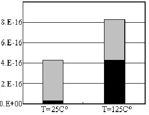
sc … (1)Where, Pleak is the leakage power dissipation, Pd is the dynamic power dissipation, Psc is the short circuit power dissipation. Pd is the dominant component of the Ptotal in the current manufacturing technologies which include Psc also. For 0.18µm technology at 100°C, leakage power dissipation is estimated to be 7% of the total power dissipation, meaning that the rest 93% is dynamic power dissipation. As the technology scales down, for the same die in a smaller technology, at the same temperature level, leakage power dissipation percentage is expected to go up as much as 50% in the future technology generation and become mortal to battery life of portable digital systems [3]. Figure 1 show the dynamic and leakage power of a 70nm CMOS inverter for different operating temperatures. The leakage power, which was initially 10% of the total power at room temperature, increases up to 49% as the temperature goes up to 125C°
Fig. 1. CMOS inverter dynamic and leakage power for different temperatures using the 70nm technology
Leakage power (Pleak) can be expressed by the equation,
age SupplyVolt Current
Leakage P
n
leak *
1
… (2)
For the static CMOS inverter, when the transistors are off, there is still some energy dissipation occurs in the circuit because of the leakage current passing through the transistors, this leakage current can be expressed by [4],
)
1
(
/
qV KTs leakage
i
e
I
… (3)Complementary Pass Transistor Control Unit
Design for Subthreshold Current Management
in Digital Portable Systems
Diary R. Sulaiman
Where, is = reverse saturation current, V = diode voltage, q = electronic charge, k = Boltzmann’s constant (1.38x10⁻²³ J/K), T = temperature [5]. Static energy dissipation is the product of the leakage current and the supply voltage from which the leakage current is drawn.
- Pd can be expressed by the equation,
clk dd L
d
C
V
f
P
2 … (4)Where, CL is the collective load capacitance, Vdd is the supply voltage, and fclk is the clock frequency.
When any transistor in the CMOS circuit makes a tran sition, the capacitances on its nodes are either charged or discharged causes dynamic power dissipation.
The dynamic power dissipation directly depends on the sizes of capacitances on the terminals of the transistors.
- Psc can be expressed by the equation,
p rf t dd sc
t
t
V
V
P
(
2
)
… (5)Where, Vt is the threshold voltage, trf is the rise time or fall time, tp is the period of the input waveform.
Psc is occurs when both the pull-up and pull-down transistors of a CMOS gate are simultaneously on.
There are three main techniques to reduce static or leakage power dissipation in microprocessors CMOS building blocks, design and implementation of low leakage transistors, dynamic threshold modulation, and finally using dual supply voltage scaling [4,5]. The CMOS operating temperature in active mode will increase due to the switching activities of the transistors that lead to amplify leakage power, and then dual supply voltage has gained a lot of attention as an efficient method to reduce total power dissipation.
During the five years ago, there are many subjects related to the topic, H. Qin in [6] presents the first analytical investigation into the voltage limit of SRAM for Low Leakage Standby Operation, M. A. Sheets in [7] presents a structured methodology and architecture for the implementation and control of power domains to form a power managed system. This paper presents a hardware design and implementation of the complementary pass transistor control unit for microprocessors subthreshold and leakage power reduction based on dual supply voltage VddL-VddH scaling at runtime depending on the workload variation; H-Leakage simulation program shows satisfactory results.
II. LEAKAGE POWER ANALYSIS
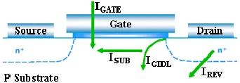
In high performance digital portable, handheld, and notebook computer architectures, the leakage component of total consumed power was increased with technology scaling, which exceeds 50% of the total consumed power [2,3]. There are four leakage mechanisms contribute to the total leakage current in a CMOS inverter as shown in figure 2,
Fig. 2. T he four main leakage components in an NMOS transistor
These four leakage current components are: - Subthreshold leakage current (ISUB)
- Gate direct tunneling leakage current (IGATE) - Reverse biased leakage current (IREV) - Gate induced drain leakage current (IGIDL)
The subthreshold leakage current (ISUB) is the main part in the four components above due to the diffusion current of the minority carriers in the channel for a MOS device. For a low input voltage in a CMOS inverter, the output will be high, in this case VGS is 0, but there is still a subthreshold leakage current passing in the NMOS transistor channel because of the Vdd potential on the VDS. Figure 3 shows the variation of the drain current of an NMOS transistor as a function of the gate voltage in 0.18m technology [8].
Fig. 3. T he drain current of an NMOS transistor as a function of the VGS
The magnitude of the subthreshold current is a function of both process, device sizing (W/L), and supply voltage Vdd. The process parameter that predominantly affects the current value is Vt. Reducing Vt exponentially increases the subthreshold current, which is proportional to VDS, or equivalently, Vdd [9].
Gate direct tunneling leakage current (IGATE) results from the Fowler-Nordheim tunneling of electrons into the conduction band of the oxide layer under a high applied electric field across the oxide layer.
IGATE depending on the tunneling probability function and the number of tunneling carriers. The magnitudes of the (IGATE) current increases exponentially with the gate oxide thickness Tox and supply voltage Vdd. As transistor length and gate oxide thickness are scaled down, supply voltage must also be reduced to maintain effective gate control over the channel region.
cause a leakage current from the drain to the substrate through the reverse-biased diode. The magnitude of this leakage current depends on the area of the drain diffusion and the leakage current density, which is in turn determined by the doping concentration [10].
Gate induced drain leakage current (IGIDL) is caused by high field effect in the drain junction of MOS transistors. For an NMOS transistor with grounded gate and drain potential at Vdd, the IGIDL is made worse by high drain to body voltage and high drain to gate voltage. IGIDL Magnitude increases as thinner oxide and supply voltage increase.
Figure 4 shows the amount leakage power prediction of the total power for the next generation CMOS technology.
Fig. 4. Leakage & total power Vs. CMOS technology scaling
A large number of CMOS circuits stay a long time in a standby mode where the leakage power is the only source of power consumption. Respond to the continuous market demand for more functionality and high processing speed while continuing to decrease the physical size and weight of the digital portable devices offer a low cost, little volume, and light weight with minimum power dissipation technology to be a primary limitation for further advancement in portable integrated circuit technologies, enhancing the necessary of the proposed circuit for subthreshold leakage current and leakage power reduction in CMOS-VLSI designs especially in digital portable systems.
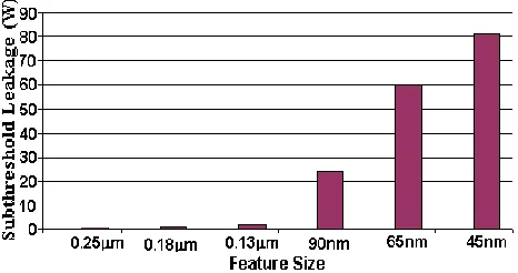
III. SUBT HRESHOLD LEAKAGE CURRENT (ISUB) Leakage power consumption has become an important factor in the design of high performance portable, handheld, and notebook processors. Process scaling has resulted in a continual reduction in the supply voltage to reduce the total power consumption and maintain circuit performance. The subthreshold leakage power trends is shown in figure 5 [10]. The subthreshold leakage current is the current that is conducted through a transistor from its source to drain when the device is intended to be off. Because of the dramatic increase in subthreshold current as shown in figu re 5, static power consumption is now one of the primary issues in deep submicron design and can account for as much as 50% of the total power dissipation for today’s processors. Then the subthreshold leakage power has become the dominant factor in the total power dissipation and battery life time due to the growing difficulty in controlling the device dimensions and characteristics.
Fig. 5. Subthreshold Leakage power trends
In the current CMOS technologies subthreshold leakage current is much larger than the other three leakage current components because of the lower threshold voltage and increasing short channel and drain induced barrier lowering effects, and is can be expressed by the equation ,
)
1
(
2 T
DS T
t GS
V V V
V V
T
sub
k
V
e
e
I
… (6)
Where, k is function of the technology, VT is the thermal voltage, Vt is the threshold voltage, VGS is the gate to source voltage, VDS is the drain to source voltage, and is the subthreshold swing coefficient [8].
It is clear from equation 6, that the reduction of threshold voltage by 100 mV increases the subthreshold leakage current by a factor of 10. Decreasing the length of transistors increases the subthreshold leakage current as well. Therefore, in a chip, transistors that have smaller threshold voltage and/or length due to process variation contribute more to the overall leakage.
Although the leakage current was important in systems with both active and inactive periods. So, the subthreshold leakage current reduction is a critical design concern in any system in today’s designs because it increases UPS or battery lifetime, reducing temperature, decreasing the production cost, and extended the IC lifetime.
Dual supply voltage scaling based to complementary pass transistor control unit design is an effective technique to reduce subthreshold current, leakage power, dynamic power (equation 4), and then the total power consumption in CMOS integrated circuits, es pecially in portable, notebook, and handheld processors at standby and varied workload conditions. As the supply adjusted between the two values VddL and VddH based on the workload prediction to complete the specific task with a targeted latency. Adjusting the supply voltage restricts the operating frequency accordingly because,
dd t dd clk
V
V
V
f
2
)
(
… (7)The reduction of the leakage power, dynamic power, and total power dissipation depending on the supply voltage adjustments are shown in figure 6 [11].
Fig. 6. Leakage power, dynamic power, and total power dissipation with supply voltage (Vdd) adjustment for a fixed clock frequency (fclk)
IV. COMPLEMENT ARY PASS TRANSIST OR CONT ROL UNIT
DESIGN BASED ON VDDL-VDDHSCALING
Microprocessors with complementary pass transistors based on dual supply voltages scaling technique have the dramatic effect on power consumption reduction when a specific computer system is in consideration; this technique can significantly reduce dissipated power without degrading speed by selectively lower supply voltage (VddL) along non-critical delay paths or light workloads and higher supply voltage (VddH) among heavy workloads. This work focuses on dual supply voltage usage. However, the same technique can be used in more than two supply voltage designs as well.
The main problem of designing dual supply voltage scaling in CMOS circuits is increasing leakage current in the high voltage gates when a low voltage gate is driving a high voltage gate. Figure 7 shows the case when a low voltage inverter is driving a high voltage inverter. [12].
Fig. 7. A low voltage inverter driving a high voltage inverter
To solve the problem of increased leakage current additional circuit of level converter is required, but it introduced area, and energy overhead. To reduce level converter problems some researchers proposed clustered voltage scaling (CVS), in such techniques no low voltage gate will drive a high voltage gate [13]. Both of these techniques introduce additional constraints to the dual supply voltage scaling process, and reducing the obtainable energy savings. Domino logic, however, does not require level shifting due to the lack of the PMOS tree in the domino gates, while the necessity to generate and route the additional supply voltages remains [14].
Other researchers introduced gate-level dual supply voltage assignment that requires the use of level shifters when a high voltage gate is driven by a low voltage gate. The level shifting circuitry in the optimized circuits constitutes 8% of the total energy consumption [15].
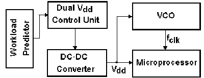
Battery-powered digital portable systems which are typically present in portable electronic devices such as cellular phones, notebook, and handheld computers, consist of the microprocessor, the DC/DC converter, voltage controlled oscillator (VCO), supply voltage control unit, and workload predictor as shown in the block diagram of figure 8.
Fig. 8. Block diagram of A battery powered system
The workload predictor unit predicts the cycles required for the next program execution tasks by calculating both the idle and event times, and then estimate the workload is it light or heavy to generate a control signal to the Vdd control unit in order to select the high or low supply voltage. The control unit of the high frequency DC-DC converter applicable to dual supply voltage CMOS circuits is presented in order to provide two voltage levels with low energy consumption.
The VCO (ring oscillator) converts the output of the DC-DC converter to a clock frequency. The DC-DC-DC-DC converter output with the generated clock frequency is fed to the processor.
There are two possible methods that can be providing switching between VddL-VddH supply voltages and control. The first method is creating by using DC-DC buck converters for each supply voltage separately as shown in figure 9.
Fig. 9. T he supply switching control using DC-DC buck converters
This method is not suitable for our proposed design because of voltage levels that produce more delay and more leakage power dissipation, and we require a change during the cycle of operation itself. Steadily a dual supply voltage can be used to provide fast and instantaneous switching between supply voltages. The second method is using two PMOS of transistors with complementary control signals that can used to select between the two supply voltages VddL-VddH efficiently.
The output of the shift registers are buffered through to generate the dual enable signals to drive the two PMOS transistors circuitry that can be separately controlled to select one of the VddL-VddH supple voltages. The complete design structure of dual supply voltage control is shown in figure 10 below,
Fig. 10. T he structure of the dual supply control unit
This structure draws current from one of the voltage supplies to drive the output by directly connecting them to the computer system microprocessor through the DC-DC converter for a period of time depending on the workload variation. VddL could be used to drive the circuit in an idle light workload state during the standby state, while VddH could be adjusted during active runtime or heavy workloads to tune the circuit block so that it only operates as fast as necessary and thus reduces active leakage currents and improves process yields. So, the proposed digital circuits can actually be configured at a minimum power level during all modes of operation. Thus, the technique balances subthreshold leakage power with dynamic switching power to reduce the overall power dissipation. Standard CMOS gates were used throughout this technique because it operates at dual or multiple supply voltages efficiently and it is very robust to noise and operating temperature. So, the battery -powered portable devices are considered to employ such dual supply voltages in the design process.
V. SIMULAT ION RESULT S
The complete hardware of complementary pass transistor control based dual supply voltage scaling of figure 10 has been designed, and then simulated Using H-Leakage simulator program depending on the A. Thomas measurement platform circuitry shown in figure 11 using the best known measure key of benchmark programs [16]. A sense resistor with a value of 0.01 Ohms is used. The voltage drop is measured across the sense resistor and amplified by the LT178 current sense amplifier and sent to the pin labeled output. This voltage can be measured by placing the probes at both the output node and the ground node.
Fig. 11. A. T homas circuit overview
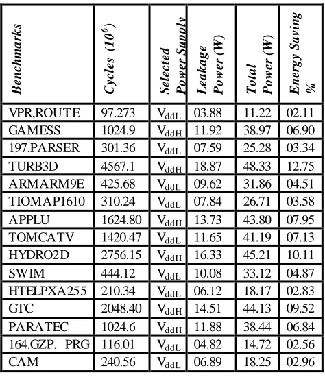
Using A. Thomas measurement platform circuit above is applied to 3.2GHz, 2.9-2.3V, 1GB SDRAM INTEL Pentium-M IV processor. The simulation results of table I are obtained using different Benchmark programs,
T ABLEI
SIMULATION RESULTS OF LEAKAGE & TOTAL P OWER CONSUMP TION USING DIFFERENT BENCHMARK P ROGRAMS.
B
e
n
c
h
m
a
rk
s
C
y
c
le
s
(
1
0
6 )
S
e
le
c
te
d
P
o
w
e
r
S
u
p
p
ly
L
e
a
k
a
g
e
P
o
w
e
r
(W
)
T
o
ta
l
P
o
w
e
r
(W
)
E
n
e
rg
y
S
a
v
in
g
%
VPR,ROUTE 97.273 VddL 03.88 11.22 02.11 GAMESS 1024.9 VddH 11.92 38.97 06.90 197.PARSER 301.36 VddL 07.59 25.28 03.34 TURB3D 4567.1 VddH 18.87 48.33 12.75 ARMARM9E 425.68 VddL 09.62 31.86 04.51 TIOMAP1610 310.24 VddL 07.84 26.71 03.58 APPLU 1624.80 VddH 13.73 43.80 07.95 TOMCATV 1420.47 VddL 11.65 41.19 07.13 HYDRO2D 2756.15 VddH 16.33 45.21 10.11 SWIM 444.12 VddL 10.08 33.12 04.87 HTELPXA255 210.34 VddL 06.12 18.17 02.83 GTC 2048.40 VddH 14.51 44.13 09.52 PARATEC 1024.6 VddH 11.88 38.44 06.84 164.GZP, PRG 116.01 VddL 04.82 14.72 02.56 CAM 240.56 VddL 06.89 18.25 02.96
The above benchmarks are used to compare the computer performance. Usually the speed of computers, in terms of the number of instructions per second, is compared using both constant supply and complementary control dual supply scaling. Benchmarks are supposed to be a standard measure of leakage power and total power for both cases.
The simulation results of table 1 shows that, the leakage power consumption is about 32.48% of the total power consumption, and the saved energy is 17.78% for the used benchmark programs.
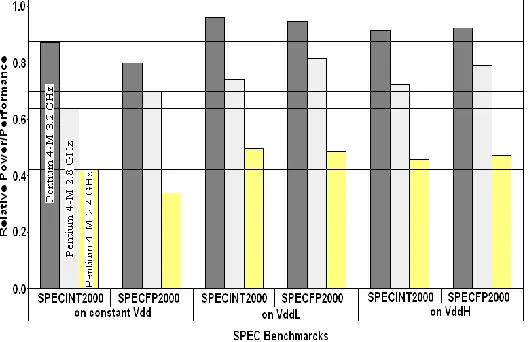
that are executed for timing purposes. The results are shown in figure 12.
Fig. 12. Relative Performance for different Laptops and Benchmarks using VddL-VddH Supply voltages
The simulation results of figure 12 shows enhanced effectiveness of the complementary pass transistor control based dual supply voltage VddL-VddH scaling of the proposed circuit, that increase the relative power/performance of the used systems for different SPEC benchmarks.
VI. CONCLUSION
In this paper a new design technique for complementary pass transistor control unit for reducing the subthreshold leakage current of digital portable systems was proposed based on dual supply voltage scaling technique, which can be considered as an effective mechanism and critical constraint for the current and future microprocessors subthreshold current and leakage/total power consumption reduction, and can improve the energy efficiency of battery -powered processor systems, especially for portable, handheld, and notebook devices.
The fully design of the proposed topology restrict the usage and problems of level converter, domino logic, and CVS circuits, and it’s also area efficient. In addition, since the proposed technique does not need multi-threshold process, it is a cheaper and hence preferable.
The H-Leakage simulation results yields that the leakage power consumption is about 32.48% of the total power consumption, and 17.78% of energy saving is achieved for the used benchmark programs.
This technique provides significant reduction in measured system energy consumption, thus significantly extending battery life.
Therefore, the proposed technique for complementary pass transistor control based on dual supply voltage scaling is becoming commonplace in high performance portable processor systems to save power and increase processing speeds.
REFERENCES
[1] M. Horowitz, T. Indermaur, and R. Gonzalez, Low-Power Digital Design, IEEE Sym posium on Low Power Electronics, pp.8-11, 1994.
[2] B. H. Calhoun, and A. P. Chandrakasan, Standby Power Reduction Using Dynamic Voltage Scaling and Canary Flip-Flop Structures, IEEE Journal of Solid-State Circuits, Vol. 39, No. 9, September 2004.
[3] Bose P., Brooks D., Irwin M., Kandemir M., Martonosi M., Vijaykrishnan N., Power-Efficient Design: Modeling and Optimizations, tutorial notes, the International Sym posium on Com puter Architecture (ISCA-28), Goteborg, Sweden, July 2001. [4] Miyatake H., Tanaka M., Mori Y., “A design for high-speed low power CMOS fully parallel content-addressable memory macros”, IEEE Journal of Solid-State Circuits, Volume: 36 Issue: 6 V pp. 956 -968, Jun 2001.
[5] N.E. Weste, K. Eshraghian, Principles of CMOS VLSI Design, 2nd
Edition, Addison Wesley Publishers, 1993.
[6] H. Qin, Deep Sub-Micron SRAM Design for Ultra-Low Leakage Standby Operation, PhD thesis, University of California, Berkeley, spring 2007.
[7] M. A. Sheets, Standby Power Management Architecture for Deep -Submicron Systems, PhD thesis, University of California, Berkeley, spring 2009.
[8] V. Kursum, Supply and T hreshold Voltage Scaling T echniques in CMOS Circuits, PhD Thesis, University of Rochester, New York, 2004.
[9] S. Sze, Physics of Semiconductor Devices, Wiley, New York, 1981. [10] Y.Lu and V.D.Agrawal, Statistical Leakage and T iming Optimization for Submicron Process Variation, In Proceedings of 20th International Conference on VLSI Design, 2007. [11] P.J.M. Havinga, G.J.M. Smit, DesignTtechniques for Low Power
Systems, Journal of Systems Architecture, Vol. 46, Issue 1, 2000. [12] Y. Cao, T . Sato, M. Orshansky, D. Sylvester, and C. Hu, New paradigm of Predictive MOSFET and Interconnect Modeling for Early Circuit Simulation, IEEE Custom Integrated Circuits Conference Proceedings (CICC’2000), pp. 201-204. 2000. [13] D. Chen, and J. Cong, Delay optimal low-power circuit clustering
for FPGAs with dual supply voltages, Proceedings of the international symposium on Low power electronics and design, ISPLED’04, USA, 2004.
[14] S. H. Rasouli, H. Koike, K. Banerjee, High -speed low-power FinFET based domino logic, Proceedings of the 2009 Asia and South Pacific Design Automation Conference ASP-DAC’09, Japan, 2009.
[15] X. Chen, Y. Wang, Y. Cao, Y. Ma, and H. Yang, Proceedings of the 14th ACM/IEEE international sym posium on Low power
electronics and design ISPLED’09, USA, 2009.