Towards a 15.5W Si-LDMOS Energy Efficient Balanced
RF Power Amplifier
for 5G-LTE Multi-carrier
Applications
B. A. Mohammed
1,2,*, A. S. Hussaini
4,5, R. A. Abd-Alhameed
1,3, I. M. Danjuma
1, A. S. Asharaa
1, I. T.
E. Elfergani
5,
and J. Rodriguez
5,61School of Engineering, Design and Technology, University of Bradford, Bradford, BD7 1DP, UK 2National Space Research and Development Agency, Abuja, Nigeria
3Depart. of Communication and Informatics Eng., Basra University College of Science and Technology, Basra 61004, Iraq 4School of InformationTechnology and Computing, American University Yola, Adamawa, Nigeria
5Instituto de Telecomunicacoes, Aveiro, Portugal 6University of South Wales, UK
Abstract
In this paper, a 15.5W Si-LDMOS balanced RF power amplifier has been designed using 2.620-2.690GHz frequency band to improve efficiency and linearity for 5G-LTE mobile applications. The amplifier was designed and simulated using large signal Si-LDMOS transistor model to achieve 53% PAE, 41dBm Pout, 14 dB gain at P1dB saturation point. The proposed
balanced RF power amplifier was fabricated and measurement results for phase variation of the signal between the carriers have been the main focus. At 1dB compression point power added efficiency increased to 81.5% with 19.5 gain at the Pout.
The AM-AM and AM-PM measured data of the balanced RF power amplifier was extracted from the MATLAB fitting tool to produce polynomials. The polynomials were used in the proposed pre-distortion technique to compensate for the nonlinearities of the balanced power amplifier. A simple linear model was designed for behavioural modelling of the memory-less baseband digital pre-distorter. A Simulink IEEE 802.11a OFDM Transceiver system was used to demonstrate validity of the proposed distorter. To the best of authors’ knowledge, this study presented excellent results of pre-distortion system that compensated the nonlinearity behaviour of the balanced RF power amplifier using the Simulink version R2011a.
Keywords: Balanced Power Amplifier (BPA); Linearity; Power Added Efficiency (PAE); Long Term Evolution (LTE); Digital Pre-distortion (DPD).
Received on 08 December 2017, accepted on 05 April 2018, published on 10 April 2018
Copyright © 2018 B. A. Mohammed et al., licensed to EAI. This is an open-access article distributed under the terms of the Creative Commons Attribution licence (http://creativecommons.org/licenses/by/3.0/), which permits unlimited use, distribution and
reproduction in any medium so long as the original work is properly cited. doi: 10.4108/eai.10-4-2018.155858
1. Introduction
In modern communication systems, frequency division multiplexing (OFDM) transceiver systems, such as long-term evolution (LTE), wideband code division multiple access (WCDMA), IEEE 802.11a OFDM Transceiver system and numerous IEEE wireless communication systems that adopt highly-efficient modulation schemes to enhance the spectral
*Corresponding author. Email: m.b.[email protected]
RF power amplifier is an important device not only in wireless communication systems but also in TV transmission, radar systems and RF heating with the amplitude of radio frequency signal increase to high value [4, 5]. Spectral efficiency and linearity are the main elements deriving the design of power amplifier. The most challenging aspect of power amplifier concept is achieving excellent efficiency with linearity [6]. Though, the design of power amplifier has to be accomplished in accordance to the system specifications, such as operating frequency, bandwidth, output power, gain, linearity, efficiency and return loss [7]. According to [8, 9], linearity is required to sustain information for error-free transmission. Efficiency reduces power consumption and improves battery lifespan at the mobile station [5, 10].
The effect of spectral re-growth in power amplifiers has become a major concern in communication systems engineering [11]. This phenomenon causes the apparent presence of nonlinearities in the frequency band which leads to transmission power loss and adjacent channel interference [3]. To reduce the effect of nonlinearity and achieve state-of-the-art system, a power amplifier must be designed carefully to increase high data rate and spectral efficiency for high-speed broadband services. The optimization of these technologies produces higher data rate and higher spectral efficiency from 20MHz signal bandwidth, with a downlink data rates of 100Mbps, and an uplink rate of 50Mbps is obtainable [5, 12].
2-way Signal Splitter
2-way Signal Combiner
Input
Internally Matched Class AB
Internally Matched Class AB
Output
50Ω Memory-less
Nonlinear Baseband Digital
Pre-distorter
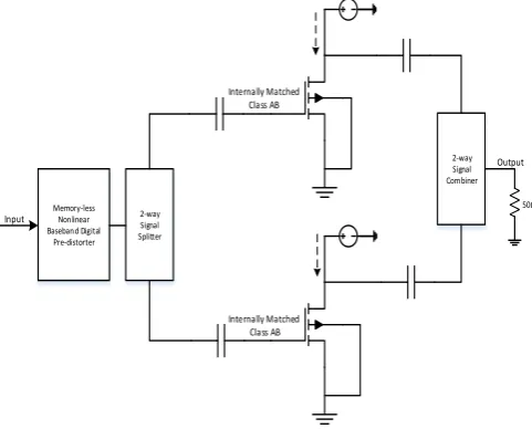
Figure 1. Balanced RF power amplifier architecture
This work discusses the design of a balanced RF power amplifier. The amplitude and amplitude-to-phase characteristics (AM-AM/AM-PM) of the amplifier used in the modelling of nonlinearities of wireless metropolitan area network IEEE 802.11a OFDM transceiver using Simulink version R2011a configuration is presented. The aim of this study is to design and implement a 5G power amplifier that can have increase in power added efficiency and respond to high linearity. This is in view of the demand to reduce power amplifier energy consumption and the need for
increase in battery life span. The objectives of this study is to design the proposed balanced RF power amplifier and implement the prototype. The design simulation and prototype measurement will be performed and compare. Amplitude and phase raw data of the proposed balanced amplifier will be extracted and converted to polynomial for linearization. A pre-distortion technique is proposed for cancellation of the proposed balanced RF power amplifier. Section 2 presents Power Amplifier Linearity, Efficiency and Output Power Requirement. The subsection 2.1 explains the Trade-off between linearity and efficiency. Section 3 describes in detail the circuit design architecture of the balanced RF power amplifier and the proposed system, while 3.1 discusses the circuit analysis of balanced RF power amplifier. Section 4 explains the design and simulation of a balanced RF power amplifier, while 4.1 presents simulation results and discussion. The design was implemented. A prototype for the balanced RF power amplifier has been shown. AM-AM and AM-PM measurement was conducted and is presented in section 4.1 respectively. Section 6 discusses the Linearization of balanced RF power amplifier Using Adaptive DPD. The section also covers the extraction and modelling of AM-AM and AM-PM polynomials in the pre-distorter. The work based on results from simulations and measurements discusses a potential technique to improve the efficiency in wide range linearity. Finally, the paper is concluded with the discussion in Section 7.
2. Power Amplifier Linearity, Efficiency and
Output Power Requirement
The 5G-LTE multicarrier systems require a more linear radio frequency amplification and higher efficiency. A balanced power amplifier is employed to provide a multicarrier signal, while putting linearity, efficiency and output power into consideration. The IEEE 802.11a standard for information technology and wireless communication systems have not identify the minimum requirement for the power amplifier intermodulation distortion. However, stated the maximum allowable intermodulation distortion in the system level requirement. These include the adjacent channel power ratio (ACPR), error vector magnitude (EVM) and envelope spectral mask (ESM).
The ACPR is the ratio between the total power transferred to the main channel and the signal power transferred to the adjacent channel. The multicarrier transmitter signal passing through the power amplifier is characterized using a complex RF band. The RF band is overwhelmed by the RF PA nonlinearity called spectral regrowth. This type of power amplifier nonlinearity is measured using the adjacent channel power ratio. There are two ways in which ACPR is measured. The first way is by defining 10*log of the ratio of the total pout
to the adjacent channel power expressed by.
.
log
10
3
3
B
A
C
P
ACPR
dBc imwhere Pim3 is the third order intermodulation distortion, C is
the number of carriers or the main channel, A is the upper adjacent channel and B is the lower adjacent channel. The measurement of the total output power and the adjacent channel power are calculated in logarithmic ratio. The second is based on the ratio of the specific output power in a less significant bandwidth around the centre of the carrier to the adjacent channel power. The smaller bandwidth is equal to the bandwidth of the adjacent channel signal, having an equivalent bandwidth of the main channel. The spectral mask is identified by the IEEE 802.11a standard as a metric for passing or failing signal at the output of the power amplifier [13]. The spectral mask provides facts about the dispersal of the modulated channel spectral energy. The test is through if the RF spectrum is within the stipulated limit defined by the mask, while the test fails if the energy level is not beyond the mask limit.
The error vector magnitude (EVM) also estimates the properties of deficiency in the communication system constellation. The error vector (E(c)) is the variation between the actual transmitted constellation point (AT(c)) and the ideal constellation point (I(c)). The error vector magnitude (EVM) can be expressed in RMS form by.
.
)
(
1
)
(
1
1 2 1
2
Nc N
c rms
c
I
N
c
E
N
EVM
(
2
)
where N is the total number of constellation points defining the level of modulation. The N is used for EVM calculation.
I(c) is the cth number of normalised constellation points and E(c) can be expressed by.
).
(
)
(
)
(
c
x
c
y
c
E
(
3
)
where x(c) is the measured normalised symbol. The rms value of the error vector magnitude is calculated by taking the average value of all the frames. In the measurement, it is recommended by the IEEE 802.11a for WLAN standard to take a large number of transmitted frames of at least 20 frames [13]. The computation of error vector magnitude for the IEEE 802.11a, WLAN standard is expressed in [13] by.
𝐸𝑉𝑀𝑟𝑚𝑠
=
∑ (√∑ (∑ {(𝑰 − 𝑰𝟎)2+ (𝑸 − 𝑸𝟎)2}
52
𝑛=1 )
𝐿𝑝
𝑣=1
52𝐿𝑝∙ 𝑃𝑎 )
𝑁𝑓 𝑎=1
𝑁𝑓 .
(4)
let 𝑰, 𝑰𝟎, 𝑸 and 𝑸𝟎 sequentially be expressed as:
[ 𝐼(𝑎, 𝑣, 𝑛), 𝐼0(𝑎, 𝑣, 𝑛), 𝑄(𝑎, 𝑣, 𝑛) and 𝑄0(𝑎, 𝑣, 𝑛)], where Nf
is the frame number, Lp is the packet data length, Pa is the average power of the constellation diagram and n is the OFDM symbol subcarrier. EVM can also be achieved in percentage by using the rms value. In the system level, it is
very important figure of merit to evaluate the precision of the OFDM signal. The EVM% can be expressed by.
%.
100
)
(
)
(
1
10
2 2
%
r N
a
er er
N
a
Q
a
I
N
EVM
f
)
5
(
where N is the number of symbols, Nr is the normalized reference of the EVM, a is the symbol index, while
I error = I reference – I measured
Q error = Q reference – Q measured
The EVM can as well be measured in decibel (dB) as expressed below.
.
log
10
10
reference error dB
P
P
EVM
)
6
(
Where Perror stands for the error vector power, and Preference is the reference constellation point power for both single and multiple carrier modulation. It is the average power of the reference constellation. In the IEEE 802.11 standard for LTE, the adjacent channel power ratio (ACPR), envelope spectral mask (ESM) and error vector magnitude (EVM) are demanding as expressed in the existing standard.
2.1. The trade-off between Linearity and
Efficiency
The aim of realizing energy efficient power amplifier with excellent linearity is to have a system with high efficiency over a magnificent range of input power. The most challenging task in RF power amplifier design is to obtain high efficiency with a wide range of linearity [14, 15]. However, achieving high efficiency with a wide range of linearity at the same time is a difficult task, except with advent of linearization and efficiency enhancement approaches. At low-level output power, high efficiency can be achieved if the efficiency enhancement method in the linear operation region of RF power amplifier is adopted. Maximum efficiency can, however, be realised once the output power of RF power amplifier reaches almost the maximum saturation level, which is the 1dB compression point. This leads to serious intermodulation distortion where efficiency drastically decreases with the decrease in output power.
output power back-off end off with a very low efficiency. A study in [12] has shown that low efficiency must be reduced to conform to the standard or will otherwise affect the operation of other applications.
However, RF power amplifier design has continued to be a challenging task when trying to satisfy this linearity-efficiency and power requirement trade-off. Previous studies have shown that there is no breakthrough in the trade-off. To optimise linearity-efficiency trade-off, more investigation is required on various power amplifier architectures.
3. Balanced RF Power Amplifier Circuit
Design Architecture
Figure 1 has shown the balanced RF power amplifier architecture. The balanced power amplifier is a cascaded system with two transistor device opposite to each other. The two amplifiers share the same input and output. They have parallel output power capability, but different in the biasing circuit. The two amplifiers are operating in class-AB with the first one in first carrier stage and the second one in second carrier stage respectively. At this point, the first carrier stage is referred to the first amplifier, while the second carrier stage refers to the second amplifier. The signal from the input is divided equally using a 3dB signal splitter. The splitter is designed with 900 phase difference and same amplitude, to
drive the two cascaded class-AB amplifiers. The output of both amplifiers are connected to a combiner which collects the amplifiers signals to the final stage of amplification [16, 17].
The balanced RF power amplifier attains high efficiency as a result of output power back-off over the traditional single stage amplifier. Hence, the multicarrier applications are affected by nonlinear distortion due to peak to average power ratio (PAPR), which the efficiency of the power amplifier can be enhanced by the used of efficiency enhancement and linearization techniques.
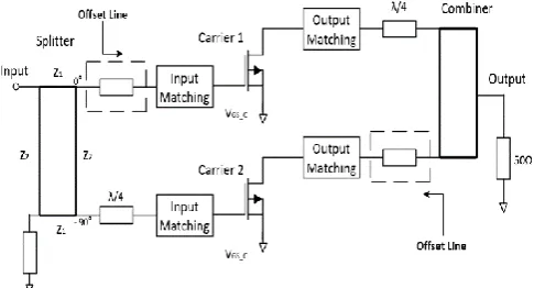
Figure 2. Proposed schematic diagram of the balanced RF power amplifier with offset lines
Figure 2 has shown a proposed balanced RF power amplifier with two amplifiers parallel to each other having equal output power capability. The two amplifiers have the
same bias point which means they are both carrier amplifier stage operating in class AB mode. The phase difference between the two amplifiers is 900 phase shift. A special signal
splitter was separately designed for the input. A coupler was also designed for the output. Independent measurements were taken in term of operational bandwidth and frequency response for both the splitter and the output coupler. In the design, no mode was chosen to behave as the carrier amplifier. Both class-AB modes operate at the same time and capable of improving the efficiency. Resonator circuits are applied to the input of the first carrier and output of the second carrier. These acts as the summing circuits which act as a phase difference signal compensator. The circuits constructively supplement the signal from the two amplifiers to the output load. The quarter-wave transmission line similarly applied to the input of the second carrier and the output of the first carrier. According to the study, the proposed balanced RF power amplifier design complexity increases and equally improve the efficiency with a wide range of linearity which will be discussed in the next section.
3.1. Balanced Power Amplifier Circuit Analysis
This section derives and demonstrates the equation that runs the relationship between input current (Iin) and input voltage (Vin) to the output current (Iout) and output voltage (Vout) in the transmission line, showing how the frequency dependent impedance of the material present the attenuation and distortion of the high-frequency signal as expressed in matrix form [14, 18].
.
2
cosh
2
sinh
2
sinh
1
2
cosh
out out o o in inI
V
z
z
I
V
)
7
(
The source impedance Zin = Vin/Iin, Zo is the characteristic impedance of the transmission line, while ZL is the load impedance given as ZL = Vout/Iout. Hence, the source impedance Zin can be expressed by.
.
2
cos
2
sin
)
(
2
sin
2
cos
o L o L inZ
Z
j
jZ
Z
Z
(
8
)
From the wave equation to the relationship between voltage and current, quarter wave transmission line source Zin can be defined by.
.
)
(
)
(
)
(
)
(
j l j lo l j l j o o in
e
e
V
e
e
V
Z
l
I
l
V
Z
)
9
(
.
l j o L o L l j l j o L o L l j o ine
Z
Z
Z
Z
e
e
Z
Z
Z
Z
e
Z
Z
)
10
(
This equation can be expanded by.
.
j l j lo l j l j o l j l j o l j l j L o in
e
e
Z
e
e
Z
e
e
Z
e
e
Z
Z
Z
)
11
(
and this can be extended in sine waveform by.
.
sin
cos
sin
cos
l
Z
l
Z
l
jZ
l
Z
Z
Z
L o o L oin
)
12
(
Finally, the impedance Zin, looking into the transmission line is given by.
.
tan
tan
l
jZ
Z
l
jZ
Z
Z
Z
L o o L o in
(
13
)
The two-stage balanced RF power amplifier is shown in figure 2 with the quarter wavelength at the output of the first carrier and the input of the second carrier amplifier respectively. These act as the basis for the impedance to stay low when the two carriers are on the active stage.
Figure 3. Current and voltage analysis diagram for balanced power amplifier
Figure 3 shows a balanced RF power amplifier analysis diagram which will be used for the current and voltage analysis. The phase output current of the first carrier (Ic1) leads the phase output current of the second carrier (Ic2) by 900. This
implies that the phase difference of the splitter is separating the two amplifiers by 900 phase shift. Nevertheless, the
operating principle of the balanced amplifier two-stage load modulation can be derived by splitting the level of input signal
to high-level drive. In this mode, first carrier (Ic1) and second carrier (Ic2) are set to be turned on and there will be current flow through the circuit. When the balanced amplifier is in ON state, the current envelope can be expressed by.
).
1
(
3
max 1x
I
I
c
(
14
)
).
1
(
3
max
2
x
I
I
c(
15
)
At high-level drive, the x component will have a value of 1, where the two carrier amplifiers will turn on. The effective impedance (ZQ) will have to pull influence on both carriers at the load as expressed below.
.
1
2
Q c L QI
I
R
Z
(
16
)
and
.
1
1 2
c Q L cI
I
R
Z
(
17
)
where the resistive impedance of the quarter wavelength increases, the two carrier amplifiers acts as load modulation. The quarter wavelength transmission line input, output transformation and the characteristic impedance can be expressed by.
.
2 1 Q x cZ
Z
Z
(
18
)
The output impedance can be substituted to the effective impedance (ZQ) and can be seen by both amplifiers. The output impedance is written as.
.
1
2 2 1
Q c L x cI
I
R
Z
Z
)
19
(
The effective output voltage (Vc1) of first carrier amplifier is expressed by.
.
1
2 2 1 1 1 1
Q c L x c c c cI
I
R
Z
I
I
Z
Since IQ = Vc1/Zx then output voltage becomes.
.
1
1 2 2 1 1
c x c L x c cV
Z
I
R
Z
I
V
)
21
(
Ic1 and Ic2 have been substituted into Zc1 to become.
1
2
.
2
2 max
1
I
Z
x
R
x
R
x
R
Z
V
x L LL x
c
(
22
)
But RL = Ropt/2. Hence the output voltage will be.
.
2
2
2
1
2 max 1
x
R
x
R
x
Z
I
R
Z
V
opt opt x opt x c)
23
(
Then Zx = Ropt
.
2
2 max 1
R
I
x
x
V
c opt(
24
)
Finally, the mathematical illustration has shown that the output voltage maintains the stability at a high stage when the two carriers remain in the active stage. The output voltage increases negligibly.
4. BPA Design and Simulation
The balanced RF power amplifier has been designed and discussed in this paper, using two transistor models for high data rate, providing efficiency with a dynamic range of linearity. Dynamic load adaptation is conveyed by the use of transmission line impedance inverter of 50Ω quarter wavelength. In the design of this amplifier, there are stages that are followed to achieve high-level performance [19, 20]. The first stage of the design is DC circuit design and simulation. Simulation of the DC circuit determines the bias point and bias network. This is in accordance with the class of operation and power requirement. The bias condition set drain-source voltage (Vds) = 28V, drain-source current (Ids) = 422mA and gate-source voltage (Vgs) = 2.7V. The bias network is designed based on class-AB carrier. The DC simulation results also indicate the class of operation. The main purpose of good biasing is to prevent signal reflection. The DC quiescent current is obtained to prevent signal distortion [5]. The radio frequency signal is prevented from going back to the DC source. For the matching network, this transistor requires no matching process, as indicated in the datasheet of the component, input and output impedance are
internally matched. The 21mm length of microstrip line are connected using line-calc from Agilent advanced design system simulator (ADS) with RT 5880 substrates, parameters; Er = 2.2, H = 0.508mm, zo = ohms, T = 3um and TanD = 0.017. The 50Ω impedance of 900 open and a short circuit is
incorporated to the right angle of the RF blocking transmission lines. A class-AB power amplifier element values have been positioned using tune tool of the ADS simulator for best performance of the proposed system.
Linear and nonlinear simulation was performed for class-AB design. The design and simulation process for class-class-AB amplifier is necessary in order to prepare the single stage class-AB design into a multiple stage balanced power amplifier. The linear simulation has shown a good flat gain, where the S11 is almost 14dB, the return loss, S11 and S22 are
also satisfactory. The nonlinear single tone simulation result of class-AB amplifier was achieved. However, it also produced up to 29% PAE at 39dBm P1dB. A 3dB 2-ways 900
hybrid splitter was designed using 100Ω impedance for optimum matching. This is to achieve 900 phase difference
between the first carrier AB and the second carrier class-AB amplifier. For a two-stage balanced PA, the first carrier and second carrier bias points are in the same mode, the input-output matching circuitry and the input-output impedances are similar as well. For the two-way splitter, various simulation tests were performed such as isolation response over the operating bandwidth, phase difference across port 2 and 1-3, and insertion loss response of the splitter [3]. From the 3dB splitter, the insertion loss achieved is reasonably low due to the high return loss, the phase difference of two signals are parallel to each other by 100Ω, which means they are separated by 900 and have equal magnitude, and the isolation
between 2 and 3, which results to -48.56dB at 2.655GHz centre frequency. Consequently, these results represent a response to protect the amplifier with all the instruments connected to it and allow measurement with reasonable accuracy. At the output of the two-stage amplifier is a combiner coupling the first carrier and second carrier amplifiers signal to the output of the balanced amplifier [3, 21].
Table 1: Performance comparison with selected work based on power amplifiers
Device Freq [MHz] PAE [%] Pout [dBm] Gain [dB] Reference
LDMOS 2655 51 41 14.6 Balanced
LDMOS 2655 29 39 15 Class-AB
LDMOS 2140 54 48.77 30 [4]
GHEMT 2655 37.14 41.18 12.78 [10]
GHEMT 2125 33.4 34.9 7.7 [11]
GHEMT 2500 48 46 13.4 [13]
LDMOS 1900 50 40 14.5 [14]
operating frequency is presented. The design presented a two-stage line-up of Doherty amplifiers, consisting of a High Voltage HBT Doherty final design cascaded with a 20W LDMOS Doherty driver, exhibiting up to 325W (55dBm) power to improve the gain to 30dB. In the case of [10] a high power hybrid envelope elimination and restoration transmitter were designed using gallium arsenide high electron mobility transistor (GaN-HEMT) at 2.655GHz operating frequency. The design introduced a conventional hybrid switching amplifier with up to 71.2% PAE. However, the efficiency of H-EER transmitter reduced to 37.04% at 41.18dBm Pout. In
[11] a conventional balanced amplifier with 90o branch line
hybrid coupler (BLHC) was used to achieve power matching rather than maximum high gain. The impedance matching is not excellent and there is inherent out-of-phase characteristic cause from the properties of 900 BLHC. To improve the
performance and correct the high signal reflection, an auxiliary amplifier was added to the conventional balanced amplifier design, only to increase the PAE to 33.4%. The design for [22] used up to 250W output power at saturation to achieve 60% drain efficiency. The final 40W GaN-HEMT Doherty power amplifier design used a digital pre-distorter to enhance linearity, as a result, experienced a reduction in PAE to 48%. Finally, in [14] a 10W, Si-LDMOS transistor power amplifier was presented with 50% PAE, 14.5dB gain achieved at 41.8dBm saturation within 1.8 to 2.0GHz operating frequency. The drawback of [14] is that heat sink is used due to excessive heating produced by the amplifier, which extensively affects the general performance of the system.
However, the current work presents a simplified balanced amplifier using Si-LDMOS transistor, while achieving up to 53% PAE, 14dB gain at 41dBm P1dB. This design is matched
perfectly due to the internal input and output matching network in the transistor device. There is no evidence of leakage or signal reflection from the first stage of the design to the design of balanced amplifier. Another advantage of this design is for its simplicity, requires no auxiliary amplifier or additional cascade Doherty device to improve the efficiency. Additional circuit accounts for extra power consumption, but have negligible impact to the overall efficiency of the amplifier [3].
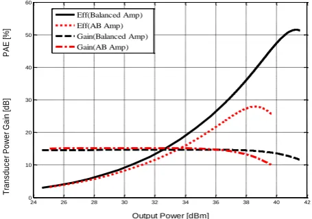
Figure 4. Simulated results of the proposed balanced RF power amplifier and conventional class AB showing PAE and gain characterization
4.1. Simulation Results and Discussion
The proposed balanced amplifier consisting of two similar class-AB amplifiers tested and simulation results are discussed. The results have shown the signal waveforms for best of performance and hence the best choice for LTE base station applications. Figure 4 shows the results of the balanced amplifier in comparison with the conventional class-AB amplifier. This indicates good performance from the balanced amplifier, achieving up to 53% PAE with 14dB gain at 41dBm P1dB, as against the conventional class-AB amplifier with 29%
PAE, 39dBm Pout and 15dB gain.
These results presented above is based on the linear simulation was conducted for the nonlinear simulation. The results obtained are the gain compression for 1dB compression point. The gain compression result is flat as expected, excellent input and output return loss was also achieved as shown in figure 4 The flat gain, S(2, 1) is almost 14 dB, the return loss, S(1, 1) and S(2, 2) was also achieved at 1 dB compression point. The results have shown quite a few kinds of signal waveforms to characterize the best of performance and the best choice for 2.620-2.690 GHz applications.
Figure 5. AM-AM and AM-PM characterization of the balanced RF power amplifier
In the one-tone nonlinear simulation test, the obtained AM-AM and AM-AM-PM characterization parameters are shown in figure 5. These are very important parameters in the characterization of PA and demonstrate that AM-AM distortion appears in a nonlinear PA, while the AM-PM distortion appears in MOSFET PA’s and produces memory effects.
5. Implementation of Balanced RF Power
Amplifier
5.1. Circuit Design Layout
The balanced power amplifier was designed and implemented using ADS software with RF field effect Si-LDMOS 15.5W transistor at 2.620-2.690GHz frequency band. The final stage circuit of the amplifier is fabricated with RT 5880 substrates,
24 26 28 30 32 34 36 38 40 42 0
10 20 30 40 50 60
Output Power [dBm]
T
ra
n
sd
u
ce
r
P
o
w
e
r
G
a
in
[d
B
]
P
A
E
[%
]
Eff(Balanced Amp) Eff(AB Amp) Gain(Balanced Amp) Gain(AB Amp)
10 12 14 16 18 20 22 24 26 28 30 32 20
30 40 50 60 70 80 90 100
Input Power [dBm]
A
M
-A
M
[
d
B
m
]
A
M
-P
M
[
D
e
g
]
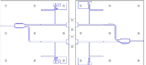
H=0.5mm and relative permittivity of 2.2. Figure 6 shows the layout of the balanced RF power amplifier. In order to experimentally verify the proposed power amplifier circuit topology, the agilent advanced design system generated microstrip layout was used. The layout was exported as Gerber files from ADS and it was milled on a printed circuit board known as PCB. Note that metal pads have been added in the layout as ground plane and power supply connection in the layout. Further, the amplifier has been subjected to following mechanical engineering:
• The length of the cooling ribs was cut to fit the card • Holes for the transistor was milled out
• A total number of 44 screw holes were threaded into the board
• 4 for the transistors
• 36 for in and outsides of the board • 4 for each SMA connectors
The screws were tried to be positioned so that they would have minimal impact on scattering field from the lines. At the same time, it was necessary to place multiple screws relatively close to the transistor in order to provide a good signal ground at this point. The same procedure was done with screws at each SMA connector. The components were fitted on the finished circuit board.
Figure 6. Design layout of balanced RF power amplifier
5.2. Circuit Prototype
The balanced RF power amplifier circuit is fabricated with RT 5880 substrates, H=0.5mm and relative permittivity of 2.2. The RT/duroid 5880 high-frequency laminate from Rogers Corporation is used. The substrate material is good for microstrip and strip-line applications. Because of the uniform dielectric constant over a wide range of frequency and the low dissipation factor of RT/duroid 5880, it extends its usefulness compared to FR-4 substrate in high-frequency Ku-band and above. The Line-Calc application from ADS is able to calculate the width and the length of microstrip line given the characteristics impedance and electrical distance or vice versa at 2.655GHz. Some important characteristics of RT/duroid 5880 such as dielectric constant, the height of board and conductivity are defined in ADS Line-Calc.
Figure 7. A prototype of the two-stage balanced RF power amplifier Fabricated with FR-4 substrate
While verifying the impedances in schematic and layout, the Gerber files are created from the layout and the circuit is milled on the RT/duroid 5880 board. During the RF operation, heat generation of the transistor would be one of the biggest problems causing performance degradation. Therefore, the transistor has to be mounted right on a heat sink in order to diffuse generated heat. In this project, a large piece of aluminium plate will be used as a heat sink and the skeleton to support the PA. The transistor is mounted on the aluminium plate with thermal paste glued in between in order to maximize heat transfer. The PA consists of two parts, the input board and the output board. SMA connectors are inserted at the input and output terminals. Banana plugs must be used for power connection as required by the competition rules. Vias are created by putting wire through drilled holes or inserting long copper tape through cut slits as connection bridges between the top and bottom ground planes. Vias should cover as much area as possible on the PA in order to provide the same reference level between the top and bottom ground planes. Components are then soldered on the board. 300pF capacitors are used as coupling capacitors at the input and output board. 1pF/1000pF/33pF capacitors are used as a decoupling capacitor in the gate bias. 1pF/1000pF/33pF/ capacitors are put in parallel and used as decoupling capacitors in drain bias.
5.3. Measurement
Figure 8. Phase variation of the proposed balanced RF power amplifier
Figure 8 shows the phase variation of the proposed balanced RF power amplifier which was derived as a function of the input power level. The result shows a range of frequency band used which is within the LTE mobile frequency level. The phases of the amplifier path are almost fixed along with bias condition throughout the range of the power used in the amplifier. There is no record of phase variation between the first carrier and second carrier in the low or high power region. The reason behind this development is because the balanced amplifier consists of same class-AB amplifiers in both carriers.
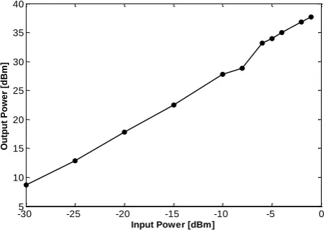
Figure 9. Output versus the input power of the balanced RF power amplifier
Nevertheless, the result shows power derive has increased at the output level when compared with that of input as the phase variation through both carriers path is almost close. It is anticipated a small drop at the full drive and both signals will look equal and disappear. The power that has been used between the input and the output of the amplifier is shown in figure 9. It represents the evaluation of the phase variation of the signal. And this clearly shows how much power has been derived through the amplifier. Up to 37dBm output power has been accomplished at the linear region of the proposed balanced RF power amplifier.
Figure 10. Measured results of the proposed balanced RF power amplifier with improved power added efficiency and gain
Figure 10 shows the performance of proposed balanced RF power amplifier through measured PAE and gain. The same frequency range of 2.620-2.690 GHz has been used for the simulation as well as the measurement. 1dB compression point of the amplifier was used to obtain up to 40dBm of the output power because of the two cascaded class-AB amplifiers working actively at the same time. However, the balanced amplifier output saturation power (Psat) point
reached up to 40.90dBm. The power added efficiency of the balanced amplifier at 40dBm and 40.90dBm were 83% and 81.5% respectively. While the gain of the amplifier reached up to 20dB which was reduced to 19.5dB before saturation point. Increase in gain and PAE improves the linearity of the amplifier. This is attributed to the input and output offset lines used in the design and fabrication. This performance shows that the design and fabrication of the proposed balanced RF power amplifier has achieved a substantial improvement in this class of power amplifiers.
6. Linearization of Balanced RF Power
Amplifier Using Adaptive DPD
In this section, the balanced RF power amplifier was linearized using the AM-AM and AM-PM transfer functions to generate polynomials in the MATLAB. The extracted AM-AM and AM-AM-PM data are measured in the context of the normalized input voltage as a function of the output voltage. The MATLAB curve fitting generated AM-AM polynomials is expressed as: a6 = 33.066, a5 = -85.52, a4 = 82.06, a3 =
-34.052, a2 = 2.85, a1 = 3.21 and a0 = -0.01. The AM-AM
distortion is effected by the device reaching a saturation point. The normalized input voltage as a function of output phase of the balanced amplifier is also considered with the following AM-PM MATLAB fitted coefficients to generate polynomials expressed as: b6 = 3.5485, b5 = -5.7836, b4 =
3.0384, b3 = -0.8434, b2 = 0.1826, b1 = -0.0225 and b0 =
0.1001. The AM-PM distortion is effected by the device reaching a saturation point. This data will be embedded in the device under test (DUT) of a simulink transceiver system
-30 -25 -20 -15 -10 -5 0
-150 -100 -50 0 50 100 150 200
Input Power [dBm]
Phase Variation [Degree]
2.620 GHz 2.655 GHz 2.690 GHz
-305 -25 -20 -15 -10 -5 0
10 15 20 25 30 35 40
Input Power [dBm]
based on IEEE 802.11a OFDM HiperLAN/2 standard. The variations of AM-AM and AM-PM can be presented in (25) and (26), expressed by:
𝑦(𝑡) = 𝑎5𝑢5+ 𝑎4𝑢4+ 𝑎3𝑢3+ 𝑎2𝑢2+ 𝑎1𝑢 + 𝑎𝑜 (25)
𝑧(𝑡) = 𝑏5𝑢5+ 𝑏4𝑢4+ 𝑏3𝑢3+ 𝑏𝑢2+ 𝑏1𝑢 + 𝑎𝑏𝑜 (26)
Where y(t) and z(t) are the AM-AM and AM-PM responses of the balanced RF power amplifier [17].
Simple linear formulas are presented for the functions involved in the amplitude and phase nonlinear models of the balanced amplifier as shown in the above equations and fit measured data very well. This model is exported to the memory-less baseband digital pre-distorter to linearize the DUT at the front-end of the OFDM transceiver system. The multiple-input-single-output (MISO) transceiver system is set to run on a simple linear model with baseband digital pre-distortion to compensate for the nonlinearity of a balanced power amplifier. In the transmitter, the signal was coded before OFDM. The modulation was normalised as a frame where 16-QAM was chosen for the OFDM system. The signal handed over to OFDM was cyclic prefixed. The OFDM as complex signal can be seen in frequency domain. The OFDM transmitter passed the complex signal to the power amplifier in the form of real and imaginary. The signal from the power amplifier is fitted in order to achieve signal variation. The amplitude of the input voltage of the power amplifier is 3volts. After the amplifier, the signal was handed over to the channel. The noise added to the channel is the Additive White Gaussian Noise (AWGN). A magnitude in +ve and -ve polarities is used to re-organise the signal which remain exactly the same. Results have been produced to show the validity of the pre-distortion algorithms used in the process of transmitting OFDM signal through the proposed balanced RF power amplifier which the measured data was extracted for linearization [23].
The amplifier has been implemented on OFDM transceiver system. Most figures of merits demonstrated the existence of amplifier distortion in the signal without linearization and several results showing removal of distortion with the use of linearization technique. The transceiver has undergo several stages of simulation such as transmission without amplifier, adding RF amplifier to demonstrate the existence of distortion and introduction of linearization technique to remove the amplifier distortion.
In the first stage, OFDM signal was transmitted to the channel without amplifier. The signal is expected to be linear with no nonlinear distortion of all kinds. No amount of distortion demonstrated in all the results simulated, unlike when adding the power amplifier in the RF chain. In the case where balanced RF power amplifier is added to the RF front-end of the transmitter, performance results have shown different ways in which the distortion was described such as display of AM-AM, AM-PM, 16-QAM constellation, bandwidth spectrum signal and OFDM signal in time scope frame.
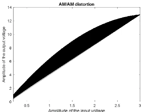
Figure 11. AM-AM distortion of the proposed balanced RF power amplifier
First of all, figure 11 and 12 depict results of AM-AM and AM-PM signal distortions of the proposed balanced RF power amplifier. The responses of the amplifier has shown clearly that the device under taste is without linearizer. The AM-AM characteristics are displayed with thousands of bits which errors were introduced because of the magnitude. Errors occurred due to variation of the magnitude. This also depends on the signal-to-noise-ratio (SNR). Hence, the errors can be reduced by increasing the level of SNR and controlling the magnitude.
Figure 12. AM-PM distortion of the proposed balanced RF power amplifier
Figure 13. OFDM transmitted and received signal constellations without linearization
Figure 14 shows the spectrum analyser figure of merit describing the OFDM frequency domain signal before and after the channel. The bandwidth and the sampling frequency used in OFDM signal shown. It shows the bandwidth that has been utilised during the transmission.
Figure 14. Spectrum signal illustrating the bandwidth
Figure 15 shows the time scope figure of merit demonstrating the OFDM complex signal in two forms which is before the power amplifier and after the AWGN channel. Each signal has been displayed with real and imaginary potion as shown below.
The first signal was obtained before the RF power amplifier and the second was after the channel. The noise added to the signal that passed through the amplifier introduced disturbance. Because of the distortion affecting the magnitude in the signal, the imaginary side of the signal after the channel is not following the imaginary side of the signal before the channel. Without distortion, the two signals are expected to demonstrate similarities. Even with increase in SNR will not make a major impact in the signal due to the distortion. This has been proven in the BER performance of the receiver side as shown in figure 22.
Figure 15. OFDM complex signal on time scope frame before linearization
The OFDM transceiver shows the BER performance of the signal received when the balanced RF power amplifier is used in the system. As shown in figure 22, the BER displayed number of bits received and the number of errors. Number of errors occurred base on amplifier distortion. However, change in SNR will change the configuration. This will affect the magnitude due to signal variation. This is to say the symbol is moving in and how to recover it is only by adapting the pre-distorter.
In the previous stage, OFDM signal was transmitted to the channel with our proposed balanced RF power amplifier where results were presented with distortions causing signal variation in the system. In the next stage, pre-distortion is introduced to linearize the nonlinearity of the RF power amplifier. In linearization, signal variation does not change the phase, but changing the magnitude and will stay where it is or on the same angle. This implies that the phase distortion is not existing in the signal. To analyse the pre-distortion, it is assume that the pre-distorter is added before the power amplifier, which means adding the phase on the signal to remove the amplitude. The pre-distorter and the power amplifier can be expressed mathematically as:
.
0
J
J
Ae
Pe
(
27
)
where
Pe
Jis the linearizer andAe
J is the PA distortion. The expression can be rewritten as:.
0
)
(
e
JPJA
PA
(
28
)
Then
.
0
AP
To cancel the RFPA distortion, we can say that
.
A
P
(
30
)
From the equations above, to compensate for the nonlinearity of the balanced RF power amplifier, a pre-distorter is added to add to the angle of the input signal. However, performance results have shown different ways in which the distortion of the power amplifier was compensated.
Figure 16. Normalized AM-AM balanced RF power amplifier pre-distorted signal
First result on linearizing the power amplifier is shown in figure 16. Figure 16 shows the normalized AM-AM response of the balanced RF power amplifier signal linearized using the pre-distortion technique. The responses of the amplifier has shown clearly that the device under taste was responding to linearization. The AM-AM characteristics are displayed with thousands of bits which errors were introduced because of the magnitude. Errors occurred due to variation of the magnitude. However, adapting pre-distorter reduced the thousands spikes and linearized the signal.
Figure 17. Normalized AM-PM balanced RF power amplifier pre-distorted signal
Figure 17 shows the normalized AM-PM balanced RF power amplifier pre-distorted signal. The performance of the pre-distorter towards figure 16 and 17 was illustrated respectively. Because of the spikes on the amplitude signal which affected the performance of the pre-distorter and cannot remove the distortion properly which has also shown not very effective impact on BER. The amplitude and phase of the amplifier were simulated by de-normalization. AM-AM and AM-PM signals were pre-distorted by not normalizing the polynomials. The performance of the pre-distorter without normalization of polynomials has improved the AM-AM signal of the amplifier.
Figure 18. Non-normalized AM-AM balanced RF power
amplifier Pre-distorted signal
Figure 18 shows the non-normalized AM-AM balanced amplifier distorted signal. The performance of the pre-distorter towards the results has improved. The spikes have been reduced, the distortion was properly reduced and the BER has improved at the receiver end.
Figure 19. Non-normalized AM-PM balanced RF power
Figure 19 shows the non-normalized AM-PM balanced amplifier distorted signal. The performance of the pre-distorter towards the results has improved more than the normalized AM-PM pre-distorted signal. The pre-distorter produced better linearization even before reaching 3 Volts at the input voltage than the one in figure 17 which is the normalized pre-distortion. However, the pre-distorter ensures no BER at the receiver end.
Figure 20. OFDM transmitted and received signal constellations after linearization
Figure 20 shows the transmitted signal before OFDM transmitter and received signal after AWGN channel. The signal constellations represent the coded 0-15 16-QAM modulation which at the transmit shows clean bits of signal without adding noise. The received signal is the signal after demodulation of the OFDM signal which can be seen as similar constellation to the transmitted signal constellation which in this case pre-distortion has been used to cancel the high distortion of the power amplifier. Pre-distorter gas made the receive signal almost close to the transmit signal.
Figure 21. OFDM complex signal on time scope frame after linearization
Figure 21 shows the time scope figure of merit demonstrating the OFDM complex signal in two forms which is before the power amplifier and after the AWGN channel.
Each signal has been displayed with real and imaginary potion as shown above. The first signal was obtained before the RF power amplifier and the second was after the channel. The noise added to the signal that passed through the amplifier introduced disturbance. Because of the distortion affecting the magnitude in the signal, the imaginary side of the signal after the channel might not follow the imaginary side of the signal before the channel. The pre-distorter has compensated the high distortion which the signals have demonstrated similarities both on real and imaginary. This has been proven in the BER performance of the receiver side as shown in figure 23. This study has been compared with some other works that was done before and were referenced accordingly. The study has relatively try to understand the knowledge of other works and improve based on facts of findings and practical experiments.
Figures 22 and 23 are the BER results that illustrated performances of the transceiver system when balanced RF power amplifier was connected and when pre-distorter was applied to the system. Both of them has practically displayed a clear proof of authenticity existence of these particular devices in action.
The OFDM transceiver shows the BER performance of the signal received when the balanced RF power amplifier is used in the system. As shown in figure 23, the BER displayed number of bits received without the number of errors. Number of errors occurred base on amplifier distortion. In this case, the errors have been removed by the pre-distorter.
The results presented in this work, to the best of author’s knowledge are potentially good efficiency and pre-distortion performance of the balanced RF power amplifier and adaptive pre-distorter used in the Simulink transceiver system based on IEEE 802.11a OFDM HiperLAN/2 standard to cancel the distortion and linearize the OFDM baseband signal.
7. Conclusion
In this study, the balanced RF power amplifier was designed and implemented. A 2.620-2.690GHz frequency band on large signal Si-LDMOS transistor model to achieve 53% PAE, 41dBm Pout, 14 dB gain at P1dB saturation point. The
proposed balanced RF power amplifier was fabricated and measurement results for phase variation of the signal between the carriers have been the main focus. At 1dB compression point power added efficiency increased to 81.5% with 19.5 gain at the Pout. The AM-AM and AM-PM measured data of
Figure 22. OFDM transceiver illustrating BER performance before linearization
Figure 23. OFDM transceiver illustrating BER performance after linearization
Acknowledgements.
This work is carried out under the grant of the Fundacão para a Ciência e a Tecnologia (FCT - Portugal), with the reference number: SFRH / BPD / 95110 / 2013. This work has received funding from the European Union’s Horizon 2020 research and innovation programme under grant agreement H2020-MSCA-ITN-2016 SECRET-722424.
References
[1] M. Helaoui, S. Boumaiza, A. Ghazel, and F. M. Ghannouchi, "Low-IF 5 GHz WLAN linearized transmitter using baseband digital predistorter," in Electronics, Circuits and Systems, 2003. ICECS 2003. Proceedings of the 2003 10th IEEE International Conference on, 2003, pp. 260-263 Vol.1.
[2] F. H. Raab, P. Asbeck, S. Cripps, P. B. Kenington, Z. B. Popovic, N. Pothecary, et al., "Power amplifiers and transmitters for RF and microwave," Microwave Theory and Techniques, IEEE Transactions on, vol. 50, pp. 814-826, 2002.
[3] B. A. Mohammed, N. A. Abduljabbar, R. A. Abd-Alhameed, A. S. Hussaini, C. Nche, M. Fonkam, et al., "Towards a green energy RF power amplifier for LTE applications," in Internet Technologies and Applications (ITA), 2015, 2015, pp. 388-392.
[4] P. Page, C. Steinbeiser, T. Landon, G. Burgin, R. Hajji, R. Branson, et al., "325W HVHBT Doherty Final and
LDMOS Doherty Driver with 30dB Gain and 54% PAE linearized to-55dBc for 2c11 6.5 dB PAR," in Compound Semiconductor Integrated Circuit Symposium (CSICS), 2011 IEEE, 2011, pp. 1-4. [5] A. S. Hussaini, T. Sadeghpour, R. Abd-Alhameed, M.
B. Child, N. T. Ali, and J. Rodriguez, "Optimum Design of Doherty RFPA for Mobile WiMAX Base Stations," in Mobile Multimedia Communications, 2012, pp. 700-705.
[6] H. Deguchi, N. Ui, K. Ebihara, K. Inoue, N. Yoshimura, and H. Takahashi, "A 33W GaN HEMT Doherty amplifier with 55% drain efficiency for 2.6 GHz base stations," in Microwave Symposium Digest, 2009. MTT'09. IEEE MTT-S International, 2009, pp. 1273-1276.
[7] Z. Wang, "Demystifying Envelope Tracking: Use for High-Efficiency Power Amplifiers for 4G and Beyond," Microwave Magazine, IEEE, vol. 16, pp. 106-129, 2015.
[8] H. Deguchi, N. Watanabe, A. Kawano, N. Yoshimura, N. Ui, and K. Ebihara, "A 2.6 GHz band 537W peak power GaN HEMT asymmetric Doherty amplifier with 48% drain efficiency at 7dB," in Microwave Symposium Digest (MTT), 2012 IEEE MTT-S International, 2012, pp. 1-3.
[9] A. A. Ismail, A. T. Younis, N. A. Abduljabbar, B. A. Mohammed, and R. A. Abd-Alhameed, "A 2.45-GHz class-F power amplifier for CDMA systems," in Internet Technologies and Applications (ITA), 2015, 2015, pp. 428-433.
IEEE 802.16e mobile WiMAX application," in Microwave Symposium Digest, 2008 IEEE MTT-S International, 2008, pp. 411-414.
[11] L. Jongsik, P. Chunseon, K. Jakyung, C. Hyeonwon, J. Yongchae, H. Sang-Min, et al., "A balanced power amplifier utilizing the reflected input power," in Radio-Frequency Integration Technology, 2009. RFIT 2009. IEEE International Symposium on, 2009, pp. 88-91. [12] A. Markos, K. Bathich, A. Tanany, D. Gruner, and G.
Boeck, "Design of a 120 W balanced GaN Doherty power amplifier," in Microwave Conference (GeMIC), 2011 German, 2011, pp. 1-4.
[13] P. Celka, N. J. Bershad, and J.-M. Vesin, "Stochastic gradient identification of polynomial Wiener systems: Analysis and application," IEEE transactions on signal processing, vol. 49, pp. 301-313, 2001.
[14] S. C. Cripps, Advanced Techniques in RF Power Amplifier Design: Artech House, 2002.
[15] F. H. Raab, "An Introduction to Class-F Power Amplifier RF Design," vol. 19, pp. 79-84, May 1996. [16] A. S. Hussaini, R. Abd-Alhameed, and J. Rodriguez,
"Design of energy efficient power amplifier for 4G user terminals," in Electronics, Circuits, and Systems (ICECS), 2010 17th IEEE International Conference on, 2010, pp. 611-614.
[17] B. Mohammed, N. Abduljabbar, M. Al-Sadoon, K. Hameed, A. Hussaini, S. Jones, et al., "A 15.5 W Si-LDMOS Balanced Power Amplifier with 53% Ultimate PAE for High Speed LTE," in International Conference on Wireless and Satellite Systems, 2016, pp. 193-201. [18] R. Kshetrimayum, Electromagnetic Field Theory,
2012.
[19] H. Sano, N. Ui, and S. Sano, "A 40W GaN HEMT Doherty power amplifier with 48% efficiency for WiMAX applications," in Compound Semiconductor Integrated Circuit Symposium, 2007. CSIC 2007. IEEE, 2007, pp. 1-4.
[20] D. Dai, L. Sun, J. Wen, G. Su, and L. Guo, "A 10W broadband power amplifier for base station," in Microwave and Millimeter Wave Technology (ICMMT), 2012 International Conference on, 2012, pp. 1-4.
[21] S. Kim, J. Moon, J. Lee, Y. Park, D. Minn, and B. Kim, "Mitigating Phase Variation of Peaking Amplifier Using Offset Line," Microwave and Wireless Components Letters, IEEE, vol. PP, pp. 1-3, 2016. [22] A. Z. Markos, D. Gruner, K. Bathich, and G. Boeck, "A
2 W GaAs doherty amplifier for 5.5-5.6 GHz applications," in Microwave Radar and Wireless Communications (MIKON), 2010 18th International Conference on, 2010, pp. 1-4.