http://www.sciencepublishinggroup.com/j/jpmt doi: 10.11648/j.jmpt.20180401.12
ISSN: 2469-8423 (Print); ISSN: 2469-8431 (Online)
Implementation of Novel Binary Logic Gates with
Temperature Stability Factor Analysis in Quantum-dot
Cellular Automata
Soudip Sinha Roy
Department of Nanotechnology, Amity University, Noida, India
Email address:
To cite this article:
Soudip Sinha Roy. Implementation of Novel Binary Logic Gates with Temperature Stability Factor Analysis in Quantum-dot Cellular Automata. Journal of Photonic Materials and Technology. Vol. 4, No. 1, 2018, pp. 8-14. doi: 10.11648/j.jmpt.20180401.12
Received: January 17, 2018; Accepted: February 5, 2018; Published: February 28, 2018
Abstract:
Quantum-dot cellular automata is a molecular logic synthesis technology which is the utmost instance for the shift of microelectronics technology towards the molecular electronics. Nowadays the quantum-dot cellular automata has been playing a major role in the list of the most emerging quantum information computation techniques. Quantum-dot cellular automata is a nanoscale information computational technology which operates through the quantum bits that are temporarily created as a result of electron tunneling in between two qdots. This is an electron configuration based device which utilizes the electrostatic repulsive force to initialize a particular binary logic state based on electronic orientation inside quantum dots. In this paper a few novel methodologies for binary logic gate designing have proposed which are highly optimized in terms of area occupancy and clock latency. Using the proposed universal gates one adjoined half adder-half subtractor, 1 bit comparator and 2 to 1 multiplexer layouts have designed. Moreover, the temperature stability factor for the proposed circuits have also analyzed to reveal the dynamic errors of the circuits during its operation. This temperature stability factor asserts that both of the proposed circuits’ adjoined adder-subtractor and the 1 bit comparator have the same operating range of temperature within 1 K to 6 K. Moreover, the cell wise power dissipation analysis for proposed gates has also performed to specify the input polarization strength limit.Keywords:
S-gates, Temperature Stability Factor, Quantum Computing, Quantum Dot Cellular Automata, Power Dissipation1. Introduction
In present quantum electronics, nowadays the quantum-dot cellular automata have been a popular nanoscale logic gate implementation technique which offers low operating latency and high computational accuracy. In artificial process inside the quantum dots the electrons are implanted precisely, which are confined by interatomic energy barrier. Those electrons are typically free but not movable in un-polarized condition. The electrons are accelerated from one quantum dot to another quantum dot by creating external electric field [1]-[4]. This device operates through quantum tunneling effect of the electrons that offers the maximum operating frequency of the device at 50 Peta Hz [3]. The electric field transfers the energy to the electrons and enforces those to be tunneled through the inter atomic trapped state (tunneling barrier) and
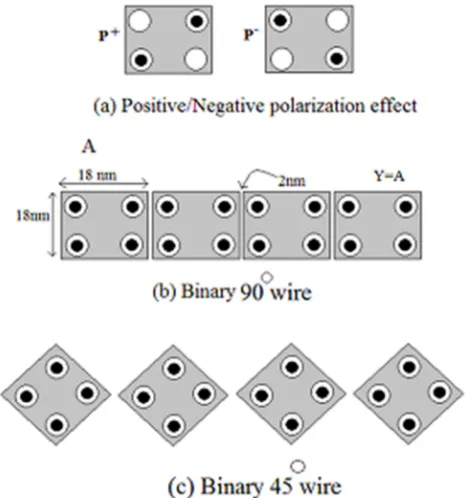
after tunneling it occupies another quantum dot temporarily. The orientation of the electrons inside the qdot defines the two binary logic states high and low. P+ originates the right handed alignment of the electrons which states binary logic state ‘1’ and the P- polarization gives logic state ‘0’, as figure 1 (a). In figure 1(b,c) the binary 90 wire and 45 wire have shown [5]-[9]. In QCA the tunneling barrier resistivity is mathematically expressed as [3],
ρ =
Whereas, d stands for the effective tunneling distance, Γ defines the tunneling rate i.e. 50 PHz, e is the electronic charge,
This paper presents some novel and optimized circuits which are named as S-gates. The proposed S gates are sophisticated enough in their designing status and the performance accuracy. The temperature stability factor has also analyzed to reveal the stability of the adjoined adder and the comparator under the temperature attack. Due to the very low temperature operability there has a probability of the electrons to get ejected from the qdots that could induce an inaccuracy in circuit performance. To resolve this complication the temperature stability analysis becomes an exigent part of circuit designing flow.
Figure 1. (a) Electron orientation under positive/negative polarization, (b) Binary 90 wire, (c) Binary 45 wire.
2. Proposed S Gates
As an emerging research field in nanotechnology, quantum-dot cellular automata (QCA) welcomes the researchers into the molecular level logic circuit designing for the vast advancement of the technology for mankind. In this research report one new gate named S-gate have been introduced which accelerates the current circuit designing flow to make that more sophisticated for further large scale logic circuit designs in QCA. In this research report six S-gates have proposed which are further convenient for very high fan out circuit planning purpose. In below figure 1, the S universal gates have proposed which consists of 6 qcells including a rotated driver cell. This S universal gate also follows the majority voter output format.
A. Proposed S-universal gates
S-universal gates are designed and configured as NAND/NOR gates which are able to provide the standard output waveform of universal gates. Both of the universal gates in figure 2 (a), have strong output strength MAX:
9.52e-001 and MIN: -9.51e-001.
B. S universal translated gates
In the next design figure 2(b), the translated cell universal gates have proposed, which consists of five qcells including translated driver cell. The translation casus a partial polarization impact on the rest cells upon the cell bed. This translation drives the signal from A and B which enriches to nand output waveform. The polarization strengths meets with the standard output polarization strengths MAX: 9.54e-001 and MIN: -9.47e-001 [10]-[14].
C. S- NOT gate
In following design S inverter gate have been planned, which is shaped by 3 cells only and the intermediate cell is partially polarized with a fixed polarization. The unite polarization is not used here to form the S-NOT gate, here +0.20 polarization is used to configure the NOT gate appropriately, figure 2(c) [7], [15]. This gate is operable with the best performance within the 0.0100 to 0.2000 fixed polarization range.
D.S-XOR gates
In figure 2(d) the S-XOR gate is proposed which is performing the binary XOR operation only through five q-cells. In this design the inputs are kept closer to make a contiguous effect of electrostatic interaction and the output is driven out from the terminal cell of the wire [16], [17]. The polarization strengths are MAX: 9.55e-001 and MIN: -9.55e-001. The horizontal wire in this layout can be extended more as per the requirement. The most effective point of this unit is the fixed polarization-less operation. In every QCA circuits the uses of the fixed polarizations causes high power dissipation on the particular cell which is skipped in this design. But this circuit avoids the large power drop by eliminating the use of FP cell.
In figure 2(e), another efficient S-XOR gate is proposed. This XOR gate is L shaped and configured by the unite polarization. The polarization strength of XOR 2 gate is MAX: 9.54e-001 and MIN: -9.55e-001.
Figure 2(f) is the ultimate design of a sophisticated XOR gate. This is the third design of a different type XOR gate. Which is appropriately configured as the binary Ex-Or gate.
Proposed three S-XOR gate layouts are sophisticated and the smallest layout have proposed ever. Above XOR unites are useful in various cases to design the large-scale circuits in QCA technology. In table I, the proposed design metrics are illustrated briefly which competes over the existing QCA logic gate designs in performance and compactness. The switching time of every designs above have computed by the following equation [3],
= (C-1)Γ
Figure 2. (a) S-NAND NOR gate, (b) S-universal gates in translated approach, (c) S-inverter gate in partially polarized technique, (d): Layout of S-XOR gate 1, (e) Layout of S-XOR gate 2, (f) Layout of S-XOR gate 3.
Table 1 Comparison of several design metrics for proposed s gates
Sr. No Design O-Cost Clock Latency Switching time (attoseconds) Area ( AUF Cost-I
1 Universal S-gates 6 0.25 0.16 4800 2.46 0
2 Universal S-translated gate 5 0.25 0.20 3840 2.37 0
3 S –Not gate 3 0.25 0.04 1600 1.64 0
4 S-XOR gate 1 5 0.25 0.12 3200 1.97 0
5 S-XOR gate 2 5 0.25 0.08 3600 2.22 0
6 S-XOR gate 3 6 0.25 0.14 4800 2.46 0.25
3. Adjoined Adder-Subtractor, 1 bit
comparator and 2:1 MUX Design
using S-gate Approach
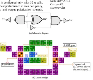
A. Proposed adjoined half adde-half subtractor is designed by S-XOR gate approach
This layout is a novel design for an adjoined adder-subtractor, figure 3, that is configured only with 32 q-cells. This circuit provides the best performance in area occupancy, cell count, clock latency and output polarization strength.
This high output polarizations stand for the high probability of the presence of the electrons in the q-dot after a logic operation. That exhibits a good precision in the layout design. It has 0.50 psec clock latency and 31200 nm which are strongly acceptable in comparison to standard design metrics. In history of QCA circuit designs this is the firstly proposed design, which has adjoined segments of adder and substrate at a very less area.
General equations: Sum/Sub= A⊕B Carry= AB Borrow= ̅B
B. Proposed 1 bit comparator using S-XOR gate and layered cells
Proposed comparator layout has been developed with the S-XOR gate practice, figure 4. In this design one XOR unite is used to shape the 1 bit binary comparator circuit. This circuit is developed with 30 qcells which has 0.50 clock latency.
Figure 4. S-gate 1 bit comparator.
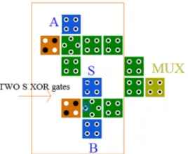
C. Proposed 2 to 1 Multiplexer layout in S gate methodology
This MUX is designed by S universal gates. The proposed MUX has shaped by 14 qcells which has 0.25 psec clock latency. Standard MUX output equation is A ̅+Bs, here A is the MSB and s is the LSB which is strictly followed by the proposed design, figure 5.
Figure 5. 2 to 1 multiplexer layout using S-universal gate.
Table 2 Comparison of several design parameters
Sr.No Design Cell used Occupied area (nm^2) Switching time (attosec) Clock latency (picosec) Cost-I
1 Adjoined adder-subtractor 32 31200 0.60 0.50 7
2 1 bit comparator 30 31200 0.56 0.50 20.50
3 2:1 MUX 14 14400 0.26 0.25 6.5
4. Temperature Stability Factor Analysis
Temperature stability factor analysis is a dynamic fault tolerance computational technique for QCA devices which can state appropriately that during the circuit operation if the temperature variation occurs then how the circuit will respond on that current temperature. The TSF analysis offers the investigation on the dynamic dependency of a QCA circuit performance (in terms of output polarization strength) on the surrounding temperature variation. The main goal of the TSF analysis is to justify and specify the circuit behavior under the temperature attack to reveal the occurred faults in the circuit output polarization strengths and to exhibit the preventing proficiency of the circuit from the output polarization strength fluctuation to escape from the unstable state of operation. The TSF analysis can provides the information about the stable operating zone of temperature for the proposed circuits. This technique has been proposed previously to show the circuit runtime behavior under temperature attack [2]. This TSF plots can explain the instantaneous output polarization strength variation due to the operating temperature moderation.
A.TSF plots for proposed S adjoined half adder and half subtractor circuit
Figure 6. TSF plot for max polarization.
In this plot it is reported that the temperature stability is the best within the temperature range of 1K to 6.5 K for S adjoined half adder and half subtractor circuit. In figure 6, the MAX polarization TSF are plotted which shows that it has a stability within 1K to 6K temperature range. Likewise, figure7 states that the stability in MIN polarizations is within 1K to 6.5K. Therefore, the entire circuit is stable under 1K to 6K temperature zone. It is shown that if the temperature is extended further than 6K then the circuit will not respond properly as desired. The reported TSF limit for this circuit is 6K.
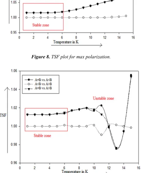
B.TSF plots for proposed 1 bit comparator circuit
Figure 8. TSF plot for max polarization.
Figure 9. TSF plot for min polarization.
Figure 8, 9 are the TSF plots for 1 bit comparator layout. This plot shows that this circuit is stable under 1K to 6K temperature but not beyond that. This recommends that this circuit is operable with maximum accuracy within the given TSF limit. The reported TSF limit for this circuit is 6K.
Figure 10. Variation in output polarization of proposed MUX under temperature attack.
Figure 11. Temperature Stability Factor analysis for proposed MUX design.
The TSF analysis asserts that the proposed 2:1 MUX circuit is stable within 1K to 7K temperature range and for further increment of operating temperature causes the miss-functionality of the circuit, figure 11.
5. Energy Dissipation Calculation for
Proposed s Universal Gate
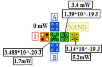
For any electronic circuit the power dissipation computation is a vital step for investigating the device dynamic behavior. The following is the power dissipation analysis for proposed S universal gate which reveals the cell wise power dissipation flow by the help of the following mathematical expression [3],
!" =#$%&&'&
(!" =)+*,- . 1 0123 45123 657 (8
driven polarization energy strength is taken 3.149 10 :;.
Figure 12. Power dissipation mapping for proposed S universal gate.
From this analysis it is found that if 3.149 10 :; of energy is used to trigger the first cell (FP) then after one iteration of the logic cycle the entire input energy is going to be dissipated till the last cell (output). This analysis asserts and specifies that the input polarization strength should always be equals or little higher than this specified polarization strength i.e. 3.149 10 :;. This is specified lowest energy strength is termed as qbit sensitizing energy.
6. Conclusion
In present nanoscale quantum information computational technologies the quantum dot cellular automata has a major role in creation of very low power and high performance molecular circuits. The QCA is being to be the mostly accepted quantum computation technology which is nowadays considered as the upcoming replacement technology for the CMOS, NMOS and other traditional binary logic synthesis technologies.
In this letter one novel gate designing technique has proposed which is named as S-gate. Here, the S universal gates have proposed and several types of efficient XOR gate layouts have proposed. By the help of the proposed S-gate unit one adjoined half adder-subtractor unite and one bit comparator have designed. The obtained layout parameters for every designs have achieved the design metrics as reported in table I, which are significantly accepted in terms of QCA circuit layout design. In section IV subsection A and B, the Temperature Stability Factor (TSF) analysis reveals the error dynamicity of the proposed adder-subtractor and the comparator circuit. The TSF analysis justifies that the both circuits adder-subtractor, 1 bit comparator are highly stable within the operating temperature zone 1K to 6K and the MUX circuit is stable within 1K to 7K temperature during temperature attack. But the further increment of temperature can lead the circuits towards the fluctuation of the output cell polarization strengths. Only within the TSF limits the circuits are considered as the stable circuit. Furthermore, the cell wise power dissipation for proposed S universal gate has also been illustrated that justifies the designing accuracy and specifies the input polarization strength rating for this circuit.
References
[1] ITRS internation trechnology roadmap for semiconductors 2011 update technical report [online] www.itrs.com
[2] Soudip Sinha Roy, “Fault Tolerance and Temperature Stability: The Dynamic Error Estimation in Quantum-dot Cellular Automata”, IEEE 3rd International Symposium on Nanoelectronic and Information Systems (iNIS), in press, doi: 10.1109/iNIS.2017.27, (2017).
[3] Soudip Sinha Roy, “Generalized Quantum Tunneling Effect and Ultimate Equations for Switching Time and Cell to Cell Power Dissipation Approximation in QCA Devices”, doi: 10.13140/RG.2.2.23039.71849, (self-publication) (2017). [4] Soudip Sinha Roy, "Simplification of master power expression
and effective power detection of QCA device (Wave nature tunneling of electron in QCA device)," IEEE Students’ Technology Symposium (TechSym), Kharagpur, pp. 272-277. doi: 10.1109/TechSym.2016.7872695, (2016).
[5] Jason R. Janulis, P. Douglas Tougaw, Steven C. Henderson, and Eric W. Johnson, Serial Bit-Stream Analysis Using Quantum-Dot Cellular Automata, IEEE Transaction on Nanotechnology, vol.3, no. 1, pp. 158-164, March 2004, DOI:10.1109/TNANO.2004.824014
[6] Gino A. Dilabio, Edmonton (CA); Robert A. WolkoW, Edmonton (CA); Jason L. Pitters, Edmonton (CA); Paul G. Piva, Edmonton (CA), “Atomistic Quantum Dots”, Pub. No. US2015/0060771 A1, 5th May 2015.
[7] K. Walus, G. Schulhof, G. A. Jullien, R. Zhang, W. Wang, “Circuit Design Based on Majority Gates for Applications with Quantum-Dot Cellular Automata”, IEEE proc. ISSN 0-7803-8622-1, pp. 1354-1357, 2004.
[8] Soudip Sinha Roy "pGate: An Introduction to A Novel Universal Gate and Power Drop Calculation of QCA circuits" International Journal Of Engineering And Computer Science (IJECS), https://www.ijecs.in, Volume 6 Issue 4, April 2017, 20967-20972, DOI: 10.18535/ijecs/v6i4.31
[9] C. S. Lent, P. D. Tougaw, W. Porod, G. H. Bernstein, “Quantum cellular automata,” Nanotechnology, vol. 4, pp. 49– 57, 1993.
[10] C. S. Lent, P. D. Tougaw, W. Porod, "Bistable saturation in coupled quantum-dot cells," Journal of Applied Physics, vol. 74, pp. 3558-3566, 1993.
[11] P. K. Rahi, S. Dewangan, S. Mirania, Md Muzaheru, “Low Power and Area Efficient Design of 1-BitCMOS Comparator Using Different Foundry”, International journal for research in emerging science and technology, vol. 2, no. 5, May 2015. [12] Lu, Yuhui & Lent, Craig, “Self-doping of molecular
quantum-dot cellular automata: Mixed valence zwitterions”, Physical chemistry chemical physics: PCCP. 13. 14928-36. 10.1039/c1cp21332f.
[14] Blair, Enrique & S. Lent, Craig, “Environmental decoherence stabilizes quantum-dot cellular automata”, Journal of Applied Physics, 113. DOI: 10.1063/1.4796186.
[15] Pulimeno, Azzurra & Graziano, Mariagrazia & Wang, Ruiyu & Demarchi, Danilo & Piccinini, Gianluca. “Charge distribution in a molecular QCA wire based on bis-ferrocene molecules”, Proceedings of the 2013 IEEE/ACM International Symposium on Nanoscale Architectures, (NANOARCH) 2013. DOI: 10.1109/NanoArch.2013.6623041.
[16] Lu, Yuhui & S. Lent, Craig. “Counterion-free molecular quantum-dot cellular automata using mixed valence zwitterions - A double-dot derivative of the [closo-1-CB9H10]- cluster”, Chemical Physics Letters, 582. 86-89. 10.1016/j.cplett.2013.07.019.
[17] QCADesigner. Accessible online at www.qcadesigner.ca/
Biography
Soudip Sinha Roy, the devoted researcher of science. He has received the B. Tech degree in Electronics and Communication Engineering from University of Engineering and Management, Jaipur, India in 2017.