Microplasma Array Serving as Photonic Crystals
and Plasmon Chains
∗)Osamu SAKAI, Teruki NAITO and Kunihide TACHIBANA
Department of Electronic Science and Engineering, Kyoto University, Kyoto 615-8510, Japan (Received 9 September 2008/Accepted 7 March 2009)
An array of microplasmas with sizes ranging from a millimeter to a micrometer, has potential for novel and promising electromagnetic-wave media, especially when the wave frequency is below the electron plasma frequency. Photonic crystals or band-gap materials composed of microplasmas have unique properties arising from their loss term, and they can become band-pass filters instead of the band-stop filters usually observed in photonic crystals of dielectrics. Such behavior is well understood using the dispersion relation in a three-dimensional space of frequency and complex wavenumber with real and imaginary parts. Another functional array is a simple one-dimensional (1D) array; it can conduct microwaves for a wide frequency range below the electron plasma frequency. The propagating modes are similar to the coupling of localized surface plasmon polaritons observed along a metallic nanoparticle chain in the photon range; however a 1D microplasma array features differ from those of a metallic sphere array, leading to a dynamic wide-band waveguide.
c
2009 The Japan Society of Plasma Science and Nuclear Fusion Research
Keywords: microplasma, electromagnetic waves, photonic crystal, surface wave, localized surface plasmon po-lariton
DOI: 10.1585/pfr.4.052
1. Introduction
Electromagnetic waves propagating in a large plasma have been explored in plasma physics for wide applica-tion to control fusion plasmas and to understand phenom-ena in the ionosphere [1, 2]. In most cases wave propaga-tion has been investigated implicitly in the region where the plasma size is larger than the wavelength of electro-magnetic waves. Plasma production for material process-ing has been also in similar regimes, where radiofrequency waves and microwaves with their wavelength less than the characteristic length of the device are the sources of power consumption or are simply coupled to a plasma capaci-tively or induccapaci-tively.
The present report investigates wave propagation where the wavelength is comparable to the characteristic length of a given periodic structure. Another important as-pect of our study is the spatial design of plasma discon-tinuities and periodicities, around which electromagnetic waves transmit and reflect due to different refractive in-dexes in both cases, and sometimes propagate as surface wave modes. Furthermore, since available plasmas in gas discharges are collisional, electron elastic collisions induce an imaginary part of the wavenumber. To study such mat-ters, this report focuses on uses of microplasmas with size ranging from a millimeter to a micrometer and electron densitiesneranges from 1012cm−3to 1016cm−3.
Periodic structure in the range of the wavelength
author’s e-mail: [email protected]
∗) This article is based on the invided talk at the 14th International
Congress on Plasma Physics (ICPP2008).
of electromagnetic waves has been well investigated as photonic crystals in photonics [3, 4], in which dielectrics are arranged periodically in two- or three-dimensional (2D or 3D) space. Band gaps and other prominent fea-tures have been observed so far. If we use microplas-mas as components of photonic crystals, the time-varying and frequency-dependent dielectric constant in plasmas is expected to add novel functions to photonic crystals. This has been proposed theoretically [5–7] and verified experimentally [8–12]. In addition, the effects of the imag-inary part of the wavenumber, which are outstanding below the electron plasma frequencyωpe, alter the functions of these band-gap materials significantly [13, 14], which will be explained in this report specifically in Secs. 2 and 3 be-low.
Another interesting phenomenon of periodic struc-tures in the photon range is a metallic-nanoparticle chain yielding a photon waveguide by coupled localized sur-face plasmons [15–17]. A similar function for conduc-tion of electromagnetic waves in the microwave range is possible along a microplasma chain below ωpe, based on the suggestions in the previous studies about surface waves on plasmas [18–24]; we reported such phenomena briefly [14]. This phenomenon is also studied in more de-tail in this manuscript in Secs. 2 and 3 below.
In Sec. 4, we discuss these two functional structures. We point out differences plasma “plasmon” chains and or-dinary metallic-nanoparticle chains; aside from the diff er-ence in frequency range, their physical properties will be compared. Also we describe the emerging conditions of
c
2009 The Japan Society of Plasma
band-gap materials and plasmon chains in a microplasma array; this discussion will clarify the requirements for fu-ture applications to high-frequency devices using these two structures.
2. Dispersion
Relations
of
Micro-plasma Array
2.1
Band gap in a complex wavenumber
plane
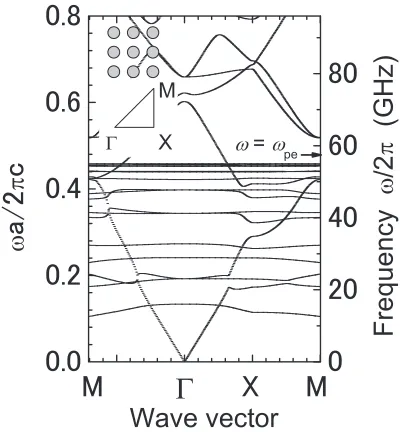
Figure 1 shows the dispersion relation of 2D wave propagation in a 2D microplasma array; in solid physics, it is called a band diagram, and the wavenumber is cho-sen as a real number. This band diagram was derived using the modified plane-wave expansion method [10], assuming that microplasmas with an electron density of 4×1013cm−3 and diameter of 1.0 mm were arranged in a square lattice of lattice constanta =2.5 mm, surrounded by a dielectric with permittivity of 3.0. The electron elastic collision fre-quencyνm was set to 0.5ωpe. When the electromagnetic wave frequencyω/2πwas aboveωpe/2π, features similar to those in band diagrams in a dielectric photonic crys-tal were observed. Belowωpe, flat bands with very low group velocity were present throughout the frequency, and a branch along the light line went across them. A band gap in theΓ-X direction was found aroundωa/2πc=0.3 along this branch. This band gap is well belowωpe, where the permittivity is less than zero, and an additional prop-erty may be present that does not occur in typical dielectric
Fig. 1 Dispersion relation (or band diagram) of microplasma ar-ray calculated by modified plane-expansion method. Mi-croplasma has a diameter of 1.0 mm with lattice constant of square lattice 2.5 mm. The shape of the profile of elec-tron density of 4×1013cm−3 resembles that in the slab
case, and the electron elastic collision frequency is set to be 0.5ωpe.
photonic crystals.
In a general collisional plasma, the loss term of elec-tromagnetic waves arising from electron elastic collisions becomes large belowωpe. Such a tendency is displayed in Fig. 2, where the imaginary part of the wavenumberkias well as the real partkr in a bulk plasma is shown in a 3D ω−kr−kispace. We assume that the permittivityεis in the Drude model, as
ε=1−ω 2 pe ω2
1
1−j(νm/ω). (1)
To derive the dispersion relation in Fig. 2, ωpe/2π is set to 57 GHz, and νm = 0.5ωpe. kr is not zero even when ω < ωpe, although the real part ofεis negative whereω2< ω2
pe+ν2m. kiis large whenω < ωpe, andkr andki are not coupled via a simple function. The resultant trajectory on the kr −ki plane is complicated, and so the propagation constant (γ=α−jβ) is very distinctive in a plasma, unlike in other solid materials.
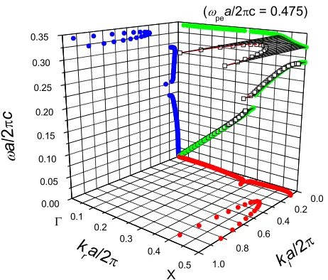
When we consider such effects resulting from the complicatedkrandkirelationship, other underlying prop-erties of lossy band gap materials can be noted. In Fig. 3, we redrew the part of the band diagram in theΓ-X direction in Fig. 1 in a similar manner to Fig. 2; not onlyω−kr but alsoω−kiwas plotted using the relationωi =−vgki[25], wherevg=dω/dkandωiis the imaginary part of the wave angular frequency derived by the modified plane-wave ex-pansion method. We also note that a number of the flat bands shown in Fig. 1 were removed, and we concentrated on the branch along the light line.
In theω−kr plane in Fig. 3, a band gap was clearly observed fromωa/2πc=0.29 to 0.32, and the dispersion relation was divided into upper and lower bands. In the lower band, there was a gap fromωa/2πc=0.17 to 0.21 arising from the crossing of one flat band, butkrandkiwere continuous on both sides of the gap. This fact indicates that this is a simple frequency band gap caused by deformation of the flat-band crossing.
Fig. 2 Dispersion relation of an infinite non-magnetized plasma in 3D space with 3 axes of real and imaginary wavenum-ber and frequency. Electron density is 4×1013cm−3, and
Fig. 3 Dispersion relation (or band diagram) of microplasma ar-ray in 3D space with parameters similar to those in Fig. 1. Data points ofkiatkia/2π >1.0 are out of range in this
figure.
However, the band gap fromωa/2πc = 0.29 to 0.32 yielded very large differences between the upper and lower bands. Althoughkr was equal on both sides atωa/2πc = 0.29 and 0.32,kiof the upper band was one order of mag-nitude larger than that of the lower band. The trajectory on thekr−kiplane clarifies that these two bands had com-pletely different properties. This is mainly attributed to dif-ferent wave-field profiles in one lattice [12]. On the upper band, wave fields concentrate on the plasma region where εis relatively small, but on the lower band, wave fields are localized outside the plasma region whereε is relatively large. If a band gap is located aboveωpe/2π, the diff er-ences in the field profile changes only the matching condi-tion between inside and outside the array regions, and the band gap shows the features of a band-stop filter [11]. On the other hand, if a band gap is located belowωpe/2π, the field profile in the periodic structure strongly affects atten-uation of the propagating waves by electron elastic colli-sions [14]. The experimental observation of this band gap will be described in Sec. 3.1.
2.2
Coupling of localized surface waves
As shown in Fig. 1, a number of flat bands are present belowωpe/2π, and they are composed of coupled modes of localized surface waves; Ito and Sakoda discussed the cou-pling conditions in the case of localized surface plasmons (LSPs) on a metal sphere in the photon range [26]. Here we show similar wave propagation by coupling of the lo-calized surface modes, and the outstanding features in the case of plasmas are addressed.Figure 4 shows the dispersion relation of 2D prop-agation in a rectangular lattice. This band diagram was derived using the direct solution of the wave equation
us-Fig. 4 Dispersion relation (or band diagram) of microplasma ar-ray determined by direct calculation of the wave equation with complex electric field. Microplasma has a diame-ter of 1.0 mm with lattice constants of rectangular lattice 3.0×7.5 mm. The profile of electron density has a peak value of 1×1013cm−3; its shape resembles that ofJ
0with
zero at the boundary.
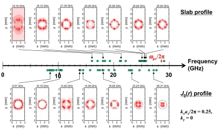
ing complex electric fields [10], and here we assumed that microplasmas with ne of 1×1013cm−3 and diameter of 1.5 mm were arranged in a rectangular lattice of lattice constantsax = 3.0 mm anday = 7.5 mm, surrounded by free space. Electron elastic collisions were neglected in this calculation for simplicity, and an electron-density pro-file consisting of a Bessel function of the first kind of the 0th orderJ0(Ar) was assumed, whereris the position from the center of the circular cross section of a microplasma, and constant A was set to fulfill the boundary condition with densityne =0 on its edge. The peak density was set to 1×1013cm−3, which was also the value in the case of the slab density profile with constantnein Fig. 5. When we in-vestigate wave propagation along a microplasma “chain,” the partial dispersion relation in theΓ-X direction is con-sidered.
At frequencies aboveωpe/2π(∼28 GHz), propagation in equivalent dielectric poles was observed. At lower fre-quencies, multiple flat bands with very low group velocity were present, similar to those in Fig. 1; this supports the existence of LSP-like modes, which will be verified later in Fig. 5. Because the bands are almost flat in theω−k di-agram, they can match various wave modes with different space impedance, which is expressed in the gradient of the ω−kplot.
Fig. 5 Spatial profiles of wave electric fields in one rectangular lattice of a microplasma array with parameters similar to those in Fig. 4.
present at up toωpe/√2; this is not consistent with the case in Fig. 5, because a microplasma in this configuration is not single but forms periodic structure that raises the upper frequency limit [12].
In the lower part of Fig. 5, profiles in the density-gradient case exhibit some features common to the slab case, but clearly different points are also found. Electric fields concentrated on the boundary of the microplasma column at low frequencies, which was similar to the pro-files in the slab case. However, as the frequency increased, localized electric fields spread into the central region. Fur-thermore, the lower limit of the wave propagation was down to 8 GHz, which was approximately half that of the slab case. These features are due to radial dependence of ωpe; because a density gradient exists in the plasma column and the characteristic length of its gradient exceeds the width of the localized electric-field profile, electric fields are present just outside the layer of “local” electron plasma frequency.
This shrinking of the localized electric-field area might give rise to change in the attenuation of transmitted waves. At higher frequencies nearωpe, there exist propa-gating modes with electric fields inside a microplasma col-umn, and their wave energy penetrates through its outer re-gion. Collisional damping and accumulated attenuation of the waves along a microplasma chain would reduce trans-mission efficiency.
3. Experimental Results
3.1
Band gap in lossy photonic crystals
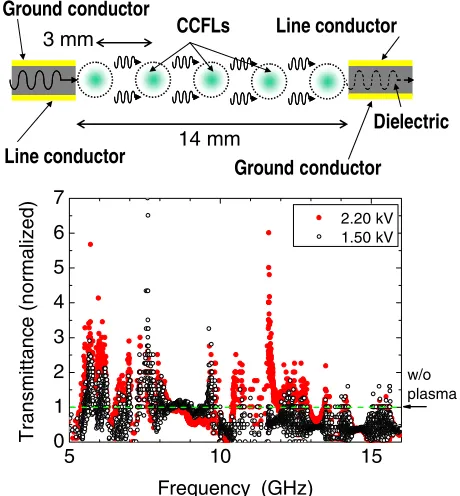
We briefly review experiments on lossy photonic crys-tals, which are described in detail in Ref. [14].A columnar plasma was confined in a fine cold cath-ode fluorescent lamp (CCFL) tube, i.e., a glass tube with an outer diameter of 1.8 mm and thickness of 0.2 mm. The discharge gas was an Ar and Ne mixture with Hg evapo-rated from liquid mercury. A bipolar square-pulsed volt-age was applied to the electrodes with an individual series resistance of 47 kΩ, and the pulse width was set to 5µs with a repetition frequency of 30 kHz. The voltage ampli-tude was 1.5-2.2 kV as a zero-to-peak value. That is, this discharge was operated in a direct-current pulse mode. Ex-perimental data for microwave transmission on microstrip and coplanar lines with an adjacent CCFL array indicated that the electron density in this columnar plasma was 0.4-1.0×1013cm−3[14], which corresponds toωpe/2πat 18-28 GHz. The CCFLs in this experiment demonstrated here were arranged between the conductors of a usual copla-nar waveguide conductors with periodic lengtha = 3.0-12.0 mm.
where wave propagation is forbidden. That is, this band-gap material works as a band-pass filter that has a pass band just below the band gap.
We point out, as a reference, the case of periodic lossless dielectrics such as photonic crystals in the pho-ton range;kr(ω) around the band gap is very similar to that shown in Fig. 3, and two frequency bands are present at the samekr(kra/2π=0.5), so that the stored energy in the elec-tromagnetic fields should differ in the two bands. Then, above the band gap, the electric fields are localized in the “air” where the permittivity is smaller, and below the band gap the electric fields are localized in the dielectric where the permittivity is larger. Inside the band gap region, the density of states is zero since their presence is forbidden, leading to a band-stopfilter. That is, both the phenomenon in lossy plasma periodic structures similar to a band-pass filter and that in a lossless dielectric periodic structure sim-ilar to a band-stop filter arise from the frequency band gap, which gives rise to the change in the field profiles.
Another aspect of the measured frequency spectra of transmitted waves leads to diagnostics of plasma parame-ters through derivation of band diagrams by surveying pa-rameters such as ne and electron temperature Te, which mainly affectskr andki, respectively; Tecan be revealed by estimation of elastic collision frequency in the Drude model.
3.2
Dynamic waveguide of a microplasma
chain
In this experiment, we also used similar CCFLs to construct a microplasma array, as described in Sec. 3.1. Here we arranged CCFLs to form a 1D array; a very simple “chain” structure.
To launch microwaves at one end of the chain and to detect them at the other end, truncated microstrip lines were set at both ends. A microwave generator (Agilent Technology, 83624B) swept frequencies from 2 to 20 GHz very slowly, in contrast to discharge voltage pulses at a 6.0-30 kHz repetition. Transmitted signals were detected by a rectifier diode and recorded in a digital storage oscil-loscope.
Figure 6 shows transmittance as a function of mi-crowave frequency. Here the definition of transmittance is similar to that in Sec. 3.1, so it indicates an enhancement factor due to plasma generation. The frequency spectrum of the transmittance shows a number of distinct and sharp peaks at 5-17 GHz; each mode of microwave propagation supported by the plasma chain was in a very narrow fre-quency region. Wwithout plasma generation, microwaves localized on the open edge of the microstrip line spread only in a near-field mode, which does not propagate as a far-field electromagnetic wave. That is, this enhance-ment of transmitted waves is attributed to wave propaga-tion along the chain of these microplasma columns.
Figure 7 displays typical time evolutions of
trans-Fig. 6 Schematic view of experimental setup and transmittance spectra at 11µs after discharge pulse. Bipolar voltage with 2.4-µs-wide square pulse is used. Time evolution of signals of transmitted waves is shown in Fig. 7.
Fig. 7 Time evolutions of signals of transmitted waves at two wave frequencies. Experimental setup was similar to that in Fig. 6.
gen-Fig. 8 Dispersion relation of surface waves on a layer withne-gradient profile. The maximumneis 1×1013cm−3. (a)α1=3×106cm−1,
(b)α1=2×104cm−1, and (c)α1=4×101cm−1. When we calculate the dispersion relation in (d), we assume a pressure term as meβ2n
e, similar to the metal case, andα1=4×101cm−1.
eration led to this signal enhancement. After the saturation of the enhanced signals, they attenuated gradually, but their attenuation rate and phase depend on wave frequency. This is partly becausenechanges in the afterglow phase after the discharge voltage is turn off; the condition of wave propa-gation on a flat band at each frequency varies one by one. Furthermore, becausekiis different in each flat band, the evolution of transmittance varies with time in a different manner.
Both experimental and numerical results strongly sug-gest that the observed microwave propagation arose from wave propagation on the LSP-like-mode chain. However, there might be other influences which would come from geometrical effects. In the experiment shown here, only five CCFLs were set, and finite array effects should be con-sidered. This finite size might also yield reflection back and forth on each CCFL, which would lead to phenom-ena like Fabry-Perot interference. Such other effects will be discussed in the future, but in practical terms this mi-crowave waveguide holds promise for forming a dynamic and flexible waveguide, independent of its physical mech-anism.
4. Discussion
Figures 4, 5, and 6 indicate that surface waves were in a wider band than surface plasmon polaritons around
a small metallic sphere forωpe/√3 < ω < ωpe/√2; on a microplasma array, numerical results indicated that sur-face waves propagated at a much lower frequency than ωpe, and transmittance enhancement, possibly by surface waves, was observed in the experiments. The numerical analysis shown in Sec. 3.2 was based on a plasma equiv-alent to a “cold” dielectric. Here we perform theoretical analysis based on the fluid model [20, 28–31], that is, a momentum balance equation including a term for electron pressurepe.
The momentum balance equation of electrons in a gas discharge is described as
mne(z)due(z)
dt =−ne(z)eE(z)− ∇pe(z) −mne(z)ue(z)νm,
(2)
where t is the time, ue the electron fluid velocity, e the charge of an electron, and E the electric field. z is set along the gradient ofne density profile. In metal optics, a similar description is referred to as the hydrodynamic formulation. Each variable is divided into static and fluc-tuating (wave-field) parts such asne = ne0+ne1, and the fluctuating part was considered to derive surface-mode dis-persion relations, although the first term of the right-hand side in Eq. (2) is approximately replaced by−ne0(z)eE1 = ε0mω2
con-tinuous change in dielectric constant with a decrease of ne0(z) down to zero, the surface waves propagating along its surface have acontinuousfrequency spectrum down to much lower frequencies thanωpe, as shown in Figs. 4 and 5.
However, a gas-discharge plasma with finite electron temperature is not the case, and we have to solve Eq. (2) with Poisson’s equation, the continuity equation, and ad-equate boundary conditions [29]. When we assume that a plasma is in the state of 1D adiabatic compression, we can setpe1(z)=3kTene1(z), wherekis the Boltzmann constant. Following the previous analyses [28, 29], we assumene0(z) profile ofω2
pe0(z)=ω2pe0(−∞)(1−cosh−
2(α1z)), whereα1 represents the surface diffuseness of thene0(z) profile, and 1/α1 is approximately the width of the electron-density gradient region in the plasma edge. That is, α1 directly affects the first term of the right-hand side of Eq. (2), and the derived dispersion relations are strongly deformed by α1.
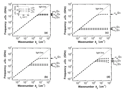
Figure 8 shows several cases of dispersion relations of surface wave modes derived from Eq. (2). Here we show the main mode saturating atωsp=ωpe/√2, the first lowest mode at a resonance frequencyω1, and the second lowest mode at a resonance frequencyω3. When we reduceα1 and make the density profile softer, the frequency spectra of the two lowest modes becomes by two orders of magni-tude lower thanωsp, as shown in Figs. 8 (a)-(c).
When we considered sheath formation on the plasma edge, the propagation mode at the very low frequencies in Fig. 8 (c) should be ruled out, since the boundary condition assumed in Ref. [29] in which polarization disappears at the edge might not be true; for instance, if we consider pe-riphery plasma withneof 1×1012cm−3, the sheath thick-ness is tens ofµm [32], which is one order of magnitude smaller than the plasma radius. As a result, the lowest fre-quency spectrum of the surface waves on a plasma in the experiment would be around 1 GHz. If we adopt a pressure term similar to that of metals, pe1(z) =meβ2ne1(z), where β2 = (3/5)v2
F and vF is the Fermi velocity [27], the fre-quency spectra of the two lowest modes remain in a range similar to that ofωsp, as shown in Fig. 8 (d). That is, the wide band of surface wave modes on the microplasma ar-ray is attributed to a soft density gradient on the edge, ex-cept for the sheath region and the pressure term in the mo-mentum balance.
In Secs. 2.1 and 2.2 we described two distinct but dif-ferent features of a microplasma array atω < ωpe. Here we briefly discuss their emerging conditions. The band gap, which occurs aroundnωa/(2πc)∼0.5, wherenis the refractive index, is clear whenahas a range similar to that of the wavelength and a significant spatial gap exists be-tween microplasmas. On the other hand, plasmon chains or flat bands in the dispersion relation are dominant when the spatial gap between microplasmas is relatively small in comparison with the wavelength and can be present at fre-quencies much less thanωpedue to its large wavenumber.
Parameters used in Figs. 1 and 4 meet such requirements for each case.
5. Summary
A microplasma array at frequencies less than ωpe serves as a photonic crystal, which is a band-gap material equivalent to a band-pass filter, and as a plasmon chain, which becomes a dynamic waveguide. We drew a band di-agram of a microplasma array in a 3Dω−kr −kispace, which clarified the band-gap properties including a fre-quency gap and attenuation discontinuity. Such features have not been noted in the previous reports of (metal-lic) photonic crystals. Plasmon chains composed of mi-croplasma arrays functioned as a dynamic waveguide, and their frequency spectra were fairly wide. Such a feature of wave propagation mainly depends on softnegradient on the edge. These microplasma array functions, verified in this report, will lead to novel wave controller devices from the microwave to the terahertz wave range.
Acknowledgments
This work was supported in part by Grants-in-Aide for Scientific Research from the Japanese Ministry of Ed-ucation, Culture, Sports, Science, and Technology, and by the Industrial Technology Research Grant Program of 2006 from the New Energy and Industrial Technology Develop-ment Organization (NEDO) of Japan.
[1] T.H. Stix, The Theory of Plasma Waves (McGraw-Hill, New York, 1962).
[2] V.L. Ginzburg,The Propagation of Electromagnetic Waves in Plasma(Pergamon Press, Oxford, 1964).
[3] E. Yablonovitch, Science289, 557 (2000).
[4] S. Noda and T. Baba, ed.,Roadmap on Photonic Crystals
(Kluwer Academic Publishing, Boston, 2003).
[5] J. Faith, S.P. Kuo and J. Huang, Phys. Rev. E 55, 1843 (1997).
[6] D.K. Kalluri, Electromagnetics of Complex Media(CRC Press, Boca Raton, 1998).
[7] H. Hojo and A. Mase, J. Plasma Fusion Res80, 89 (2004). [8] O. Sakai, T. Sakaguchi and K. Tachibana, Appl. Phys. Lett.
87, 241505 (2005).
[9] O. Sakai, T. Sakaguchi, Y. Ito and K. Tachibana, Plasma Phys. Control. Fusion47, B617 (2005).
[10] O. Sakai, T. Sakaguchi and K. Tachibana, J. Appl. Phys. 101, 073304 (2007).
[11] T. Sakaguchi, O. Sakai and K. Tachibana, J. Appl. Phys. 101, 073305 (2007).
[12] O. Sakai and K. Tachibana, IEEE Trans. Plasma Sci.35, 1267 (2007).
[13] O. Sakai, T. Sakaguchi, T. Naito, D.-S. Lee and K. Tachibana, Plasma Phys. Control. Fusion49, B453 (2007). [14] T. Naito, O. Sakai and K. Tachibana, Appl. Phys. Express
1, 066003 (2008).
[15] J.R. Krenn, A. Dereux, J.C. Weeber, E. Bourillot, Y. Lacroute, J.P. Goudonnet, G. Schider, W. Gotschy, A. Leitner and F.R. Aussenegg, Phys. Rev. Lett. 82, 2590 (1999).
Rev. B62, R16356 (2000).
[17] S.A. Maier, P.G. Kik, H.A. Atwater, S. Meltzer, E. Harel, E., B.E. Koel and A.A. Requicha, Nature Mat. 2, 229 (2003).
[18] A.W. Trivelpiece and R.W. Gould, J. Appl. Phys.30, 1784 (1959).
[19] J.C. Nickel, J.V. Parker and R.W. Gould, Phys. Rev. Lett. 11, 183 (1963).
[20] J.V. Parker, J.C. Nickel and R.W. Gould, Phys. Fluids7, 1489 (1964).
[21] H.C. Hoh, Phys. Rev.133, A1016 (1964). [22] D.J. Cooperberg, Phys. Plasmas5, 862 (1998). [23] Y. Yasaka and H. Hojo, Phys. Plasmas7, 1601 (2000). [24] I.P. Ganachev and H. Sugai, Surf. Coat. Technol.200, 792
(2005).
[25] K.C. Huang, E. Lidorikis, X. Jiang, J.D. Jannopoulos, K.A. Nelson, P. Bienstman and S. Fan, Phys. Rev. B69, 195111 (2004).
[26] T. Ito and K. Sakoda, Phys. Rev. B64, 045117 (2001). [27] F. Forstmann and R.R. Gerhardts,Metal Optics Near the
Plasma Frequency(Springer-Verlag, Berlin, 1986). [28] A. Eguiluz and J.J. Quinn, Phys. Rev. B14, 1347 (1976). [29] J.E. Sipe, Surf. Sci.84, 75 (1979).
[30] C. Schwartz and W.L. Schaich, Phys. Rev. B 26, 7008 (1982).
[31] J.M. Pitarke, V.M. Silkin, E.V. Chulkov and P.M. Echenique, Rep. Prog. Phys.70, 1 (2007).