Nanometer-Scale Patterning on PMMA Resist
by Force Microscopy Lithography
Sadegh Hassani, Sedigheh*+; Sobat, Zahra; Aghabozorg, Hamid Reza Catalysis Research Center, Research Institute of Petroleum Industry (RIPI),
P.O. Box 18754-4163 Tehran, I.R. IRAN
ABSTRACT:Nanoscale science and technology has today mainly focused on the fabrication of nano devices. In this paper, we study the use of lithography process to build the desired nanostructures directly. Nanolithography on polymethylmethacrylate (PMMA) surface is carried out by using Atomic Force Microscope (AFM) equipped with silicon tip, in contact mode. The analysis of the results shows that the depth of scratches increases with the increase of applied normal force. The scanning velocity is also shown to influence the AFM patterning process. As the scanning velocity increases, the scratch depth decreases. The influence of time and number of scratching cycles is also investigated.
KEY WORDS: Nano-lithography, Nano-patterning, Force lithography, Atomic force microscopy, Scanning probe lithography.
INTRODUCTION
Scanning Probe Microscopy (SPM), such as Scanning Tunneling Microscopy (STM) and Atomic Force Microscopy (AFM) has become a standard technique for obtaining topographical images of surface with atomic resolution [1]. Much research has been performed regarding the application of such SPMs to semiconductor processing taking advantage of the high resolution and alignment accuracy [2,3]. Therefore, allowing the fabrication of reliable nanometer scale electronic devices, which could not be achieved by conventional lithographic techniques [4,5]. Most popular SPM lithographic techniques are resist film lithography and lithography by oxidation [6,7]. An interesting way of performing nanometer pattern is direct scratching of the sample
surface mechanically by the probe [8,9]. This method has the advantage that is not restricted to conductive materials [10].
Garcia et al. have described a review of various lithographic methods by AFM [11,12]. The AFM nano-lithography technique takes advantages of the imaging facility and the ability of moving a probe over the sample in a controllable way [13]. For this purpose, AFM head employs an optical detection system in which a laser beam is focused onto the backside of a reflective cantilever and is reflected from the cantilever onto a sensitive photo detector.
Variation in the height of the surface leads to deflection of the cantilever spring, which is directly
*To whom correspondence should be addressed.
+E-mail:[email protected]
proportional to the tip-sample interaction force [14]. The normal force between tip and sample is estimated from cantilever deflection (nA) curve plotted against Z-displacement of the cantilever and converting this curve to Force-Distance curve [15-17].
To apply force optimally for making nanoscratches, we require to understand underlying behavior and parameter that control it, a tip which is optimized for applying force under the experimental conditions, and scanning techniques which allows one to use these tips and retain desired properties [18].
In this work, the nanolithography is performed on the polymeric surface by atomic force microscope. The investigation of direct writing, where the AFM probe “scratches” a polymeric surface, is reported. For scratching we mean the mechanical action of the tip that is used as a sharply pointed tool in order to produce fine scratches. The direct scratching is possible with high precision but low quality results are obtained due to probe wear during lithographic process.
Before lithography performance, a soft thin film of PMMApolymeronthe silicon substrate is prepared. Since its hardness is much less than silicon, the direct resistless formation of nanoscratches could easily be achieved.
Various important factors such as, magnitude force, time, number of scratching cycle and velocity of scanning are studied.
EXPERIMENTAL
All the nanolithographic process and imaging in this paper are performed on silicon substrate, which is covered by PMMA (LG-IH830), thin film.
A commercial atomic force microscope (Solver P47 H, NT-MDT Company) operated in contact and non-contact modes, equipped with a NSG11 cantilever is used to perform the lithography of PMMA layer.
The cantilever made of silicon nitride, has a rectangular shape, and its lengths, widths and thickness are 100 ± 15 µm, 35 ± 3 µm, and 1.7-2.3 µm respectively. Its normal bending constant measured by supplier is 11.5 nN/nm. This probe is sufficient to reach plastic deformation of PMMA and also for obtaining good image of scratches. To prepare the surface for nanolithography, silicon surface is washed and sonicated in acetone/ethanol (50-50 % vol) for 15 minutes at room temperature. For making PMMA thin film, a very small amount of diluted
PMMA/CHCl3 solution is coated over silicon surface
by using spin coater with 6000 rpm for 30 seconds. Then the coated substrate is dried in an oven at 130 oC for 30 minutes. The thickness of this coated layer is 150 nm, measured by atomic force microscope.
The lithography process is executed with the use of lithography menu supported by the microscope software. The AFM tip is brought into contact with the sample surface using the smallest force possible to minimize any undesired surface modification. An image of the PMMA surface is prepared in order to choose a suitable area free of defects for lithography. Then the nanolithography process is executed under various specific and controlled conditions to analyze the effect of lithography important factors on the shape of scratches.
For analyzing force effect, the AFM is operated in contact mode with a normal force (F) ranging from 1300 to 3510 nN. For AFMscratching,theforceis increased by applying a higher voltage to the piezo-scanner in order to reach the cantilever deflection ( Z) corresponding to the force (F) range where plastic deformation of PMMA occurs.
These compared to “imaging”, much higher forces are achieved by accordingly increasing the applied voltage to piezo scanner. From the cantilever deflection (∆Z), the forces are calculated using Hook’s law (F= K∆Z).
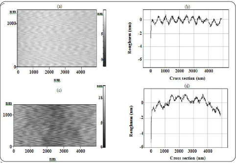
Fig. 1: The evolution of the topography image and profile of (a, b) silicon surface after cleaning, (c, d) PMMA thin film.
the contact mode is chosen to image the scratches, they are probably damaged because of soft surface of PMMA.
RESULTS AND DISCUSSION
In order to choose suitable area for nanolithography process, the roughness of the film is studied with the AFM. InFig.1theevolution of the topography image and profile of the silicon surface after cleaning (a, b) and PMMA thin film coating (c, d) are presented. It’s seen that the roughness is low and surface profile of PMMA layer is appropriate for lithography. An accurate study is performed on this sample in order to find the optimum patterning conditions for the PMMA film.
Nano scratches are created using the AFM tip. The main factor in pattern formation is the magnitude of the force applied to the sample. The influence of the normal applied force has been investigated on silicon covered by the PMMA film.
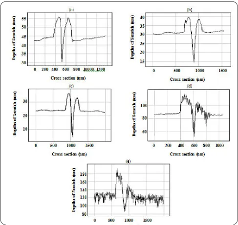
In Fig.2(a-e)someofsurfaceprofileof nano scratches arepresented,whichareformedwiththeconstant scanning
velocity 140 nm/s, number of scratching cycle 10, time 25 ms, and at the various forces (2350, 2700, 3050, 3400, and 3510 nN). These profiles indicate that the increase of normal applied force leads to the deeper scratches.
The scratches show a V-shape, however protrusions are visible along some of the scratches indicating the presence of permanent deformation. We find that the optimum value for normal applied force is about 3050 nN. The scratch made by this force is shown in Fig. 3.
In Fig. 4, the scratch depths are plotted as a function of the normal applied force. As expected, the scratch size increases with force load. The depth varies from 4 to 32 nm by increasing force load from 1300 to 3510 nN. However due to the convolution effect of the tip and substrate topography, the scratch depth may appear smaller by AFM imaging than their actual size [19].
Fig. 2: a-e) Surface profile for scratched PMMA layer. (N= 10 cycles, T=25 ms and V=140 nm/s) and F is: (a) 2350 nN, (b) 2700 nN, (c) 3050 nN, (d) 3400 nN and (e) 3510 nN.
Fig. 3: Topography images of the scratch performed at N= 10 cycles, T=25 ms, V=140 nm/s and F= 3050 nN. ((a) two dimensional image and (b) three dimensional image)
Cross section (nm)
(a) (b)
nm 30
20
10
nm 30
20
10 nm
20 500
0
0 1000 2000
3000 4000
nm
Fig. 4: Dependence of the scratch depth to the normal applied force. The time, number of scratching cycle and scanning velocity are: 25 ms, 10 and 140 nm/s respectively.
Fig. 5: Dependence of scratch depth to the number of cycles (N). The normal applied force, scanning velocity and time are 2350 nN, 140 nm/s, and 25 ms respectively.
applied force 2350nN, scanning velocity 140 nm/s and time 25 ms is presented. This figure shows that the depth varies from 4 to 30 nm by increasing the number of cycles. As expected, the depths of scratches increase with N linearly. This linear relationship between depth and number of cycles confirms layer-by-layer removal mechanism, which was presented by Santinacci and co-workers [20].
The influence of the scanning velocity on the lithography pattern, taken at a normal force of 2350 nN is presented in Fig. 6. As it is shown in this figure, the depth varies from 24 to 8 nm by decreasing scanning velocity from 140 to 540 nm/s. It is observed that the increase of the scanning velocity induces a decrease in the scratch depth. Thus, slower scans seem to generate higher
Fig. 6: The influence of the scanning velocity on the depth of the lithographed pattern. The normal applied force, time and number of cycle are 3125 nN, 25 ms and 10 respectively.
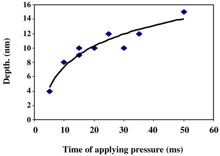
Fig. 7: The indentation depth as a function of the time of
applying pressure. Thenormal applied force, scanning velocity
andnumberofcycle are 2350 nN, 140 nm/s and 10 respectively.
pressure and as a result deeper scratch pattern are obtained. However, we could not determine whether the depth decreases linearly or exponentially with the increase of the scanning velocity (see Fig. 6).It has to be noted that the low scanning velocity is a limiting factor of final throughput (number of patterns per hour), however results in better patterns in nanolithography.
To analyze the time effect, nano-indentations are performed on the PMMA surface. The indentation depth as a function of the time over which the constant force is applied has been presented in Fig. 7.
In this case, prior to unloading, the load is held constant for periods ranging from 5 to 50 ms. It can be seen in Fig. 7 that by increasing the time (of applying pressure), indentation depth is increased. The increase of
35 30 25 20 15 10 5 0 D ep th . ( nm )
1000 1500 2000 2500 3000 3500 4000
Force (nN) 35 30 25 20 15 10 5 0 D ep th . ( nm )
0 5 10 15 20 25 30 35
Number of cycles (N)
30 25 20 15 10 5 0 D ep th . ( nm )
0 1000 2000 3000 4000 5000 6000
Velocity (Å/s) 16 14 12 10 8 6 4 2 0 D ep th . ( nm )
0 10 20 30 40 50 60
the lithography depth with the loading time shows that the plastic deformation on the PMMA film is time dependent. In this case, to accumulate the tip-induced stress, dilation changes such as defects created or absorbed near the vicinity of the deformed region on the surface occur. This effect leads to an additional plastic deformation of the film.
CONCLUSIONS
This paper summarizes the study of the force microscopy lithography process which includes, the deposition of PMMA thin film by use of spin coater on a silicon substrate, and the use of the atomic force microscope to draw a pattern, in a controlled way, on the surface of PMMA layer.
The analysis of the roughness of the surface shows that the concept using a thin insulting layer of PMMA on silicon surfaces as a scratching mask can be successfully performed for nanopatterning.
The necessary parameters to control the drawing procedure on the PMMA layer are analyzed. It was shown that the depth of the lithography mark increases with the increase of the applied normal force with a linear trend.
It is presented that the increase of the scanning velocity induces a decrease in the scratch depth. The increase of the lithography depth with the loading time suggests that the plastic deformation on PMMA layer is time dependent. In this case, to accumulate the tip induced stress, dilation changes such as defects created or absorbed near the vicinity of the deformed region on the surface might occur, which would lead to an additional plastic deformation of the film.
The influence of the number of scratching cycle in the drawing of the lithography pattern is also investigated. It is shown that the depth of the lithography mark increases with the increase of the number of scratching cycle.
Acknowledgements
We are grateful to the National Iranian Oil Company (NIOC) for financial support, which enabled this work to be undertaken. We would also like to thank Dr. M.M. Ahadian and Miss M. Davoodi for their good cooperation. Acknowledgements are also addressed to Mrs. Ekaterina Alexeeva (from NT-MDT company), for her helpful guidance.
Received : 13th July 2007 ; Accepted : 2nd June 2008
REFERENCES
[1] Hyon,C.K., Choi, S.C., Hwang, S.W., Ahn, D., Kim, Y. and Kim, E.K., Appl. Phys. Lett., 75(2), 292 (1999).
[2] Martin, C., Rius, G., Borrise, X. and Perez-murano, F., Nanotechnology, 16, 1016 (2005).
[3] Sheehan, P.E. and Whitman, L. J., Physical Review Letters, 88, 156104 (2002).
[4] Lyuksyutov, S.F. Paramonov, P.B., Juhl, Sh. and Vaia, R.A., Applied Physics Letters, 83, 4405 (2003).
[5] Lyuksyutov, S.F., Paramonov, P.B., Sharipov, R.A. and Sigalov, G., Physical ReviewB, 70, 174110 (2004).
[6] Sheglov, D.V., Latyshev, A.V. and Aseev, A.L., Applied Surface Science, 243, 138 (2005).
[7] Sugimura, H., Uchida, T., Kitamura, N. and Masuhara, H., Appl. Phys. Lett., 63, 1288 (1993). [8] Lyuksyutov, S.F., Paramonov, P.B., Dolog, I. and
Ralich, R.M., Nanotechnology, 14, 716 (2003). [9] Park, J. and Lee, H., Material Science and
Engineering C, 24, 311(2004).
[10] Fonseca Filho, H. D., Mauricio, M. H. P., Ponciano, C.R. and Prioli, R., Material Science and Engineering B., 112, 194(2004).
[11] Geissler, M. and Xia, Y., Adv. Mater., 16, 1249 (2004).
[12] Garcia, R., Martinez, R. V. and Martinez, J. Chem. Soc.Rev., 35, 29(2006).
[13] Samori, D., Chem. Soc. Rev., 34, 551 (2005). [14] Heimberg, J. A. and Zandbergen, H. W., Phys. Rev.
Lett., 92(12),126101 (2004).
[15] Yeung, K.L.N. and Yao, J., Nanosci. Nanotechol.,
4, 1 (2004).
[16] Carallini, M., Biscarini, F., Leon. S., Zerbetto, F., Bottari, G. and Leigh, D.A., Science 299, 531(2003). [17] Santinacci, L., Zhang, Y. and Schmuki, P., Surface
Science, 597(1-3), 11 (2005).
[18] Yasin, Sh., Khalid, M.N., Hasko, D.G., and Sarfraz, S., Microelectronic Engineering, 78-79, 484 (2005). [19] Sadegh Hassani, S. and Ebrahimpoor Ziaie, E.,
Materials Science: An Indian Journal, 2 (4-5), 134 (2006).