© 2016 IJSRSET | Volume 2 | Issue 3 | Print ISSN : 2395-1990 | Online ISSN : 2394-4099 Themed Section: Engineering and Technology
Study and Review on VLSI Design Methodologies and Limitations using
CMOS Adder Circuits
Niranjan Kumar, Vipul Aggarwal
Department of Electronics and Communication Engineering, Trinity Institute of Technology and Research Bhopal, Madhyapradesh, India
ABSTRACT
In this review paper different design techniques of multi bit adder are deliberate using linear parameters logic gates. The comparison is carried by several parameter mainly focus on a number of linear threshold gates, a number of CMOS transistor, power dissipation, power delay product (PDP), average power dissipation time delay and size of the full adder circuit. Adder circuits basically implemented using basic logic gates namely XOR and AND gates. Half Adders or Full adders may be realized in various ways depending on the various process technologies and design methodologies deployed for making these digital integrated circuits design. The Full adder, 14T, pseudo-nMOS, MULTIPLEXER-BASED FULL ADDER , 8T, Inverter-based full-adder with pass transistors, Conventional CMOS (C-CMOS), 20T,10Twith 4T-XNOR, 6T, 16T, 9T, Double gate MOSFET and hybrid 1-bit full adder full adders etc
Keywords: CMOS, Adders, VLSI Design, CAD, process technology, delay analysis
I.
INTRODUCTION
In this paper, a full adder design employing both complementary metal–oxide–semiconductor (CMOS) logic and transmission gate logic is reported. The design was reviewed firstly implemented for 1 bit and then extended for 32 bit also. The circuit was implemented using many professional VLSI CAD such as Cadence Virtuoso tools in 180-and 90-nm technology. Performance parameters such as power, delay, and layout area were compared with the existing designs such as complementary pass-transistor logic, transmission gate adder, transmission function adder, hybrid pass-logic with static CMOS output drive full adder, and so on. For low power voltage supply at process technology below 180-nm technology, the average power consumption few µW less than 10 µW was found to be extremely low with moderately low delay less than 200 ps resulting from the deliberate incorporation of very weak CMOS inverters coupled with strong transmission gates. Corresponding values of the same were 1.17664 µW and 91 The design was further extended for implementing 32-bit full adder also, and was found to be working efficiently with only
variable and contant delay logic styles and power tabulated at 180-nm (90-nm) technology for 1.8-V (1.2-V) supply voltage. In comparison with the existing full adder designs, the present implementations were found to offer significant improvement in terms of power and speed and overall performance as well.
[1,8]The chip design process enforced the automation of process, automation of simulation based verification i.e. replacing of traditional breadboard techniques through HDL (hardware description language) development. The various modular hierarchical techniques of design created the scenario that CAD tools are inevitable [11].
II.
METHODS AND MATERIAL
A. VLSI Technology and Design
A VLSI System integrates millions and millions of electronic components in a small area. The main objective is to make the analog or digital system as compact as possible with the required functionalities. Tens and thousands of transistors are fabricated on a small piece of wafer. The circuits are tested and fabricated because once an error is created the whole design is waste and it costs million and millions of dollars. Therefore CAD tools came into the picture. CAD tools are inevitable.[9] This chip design forced automation of process, automation of simulation based verification. This CAD assistance has led to Electronic Design Automation.
B. Design Methods
Systematic design methods or the design methodologies are necessary for successfully designing complex digital hardware.
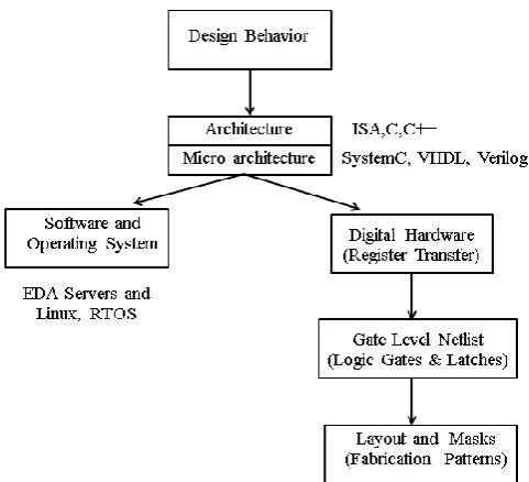
Figure 1. Abstraction Hierarchy for VLSI Adders 1 Our design methods usually differ by the number of abstraction levels and the complexities involved.
Figure 2. Abstraction Hierarchy of VLSI Adders 2
Comparing structurally different views of a VLSI Design include divide and conquer techniques which includes sorting by structure and sorting by issues. The design hierarchy that uses existing techniques has an unacceptable restriction that they use identical hierarchies. Structurally hierarchy transformation is the first step and hierarchy base comparison is the last step.
Figure 3. Design representation levels and formats associated
A. Structured Design Techniques B. Programmable Logic Design C. Gate Array and Sea of Gates Design D. Cell Based Design
E. Full Custom and Semi-custom Design F. Platform based Design and SOC More levels of abstraction
Less levels of abstraction
C. Adder Designs using various Technologies
There are numerous topologies and designs exist in literature. Few of them are as follows
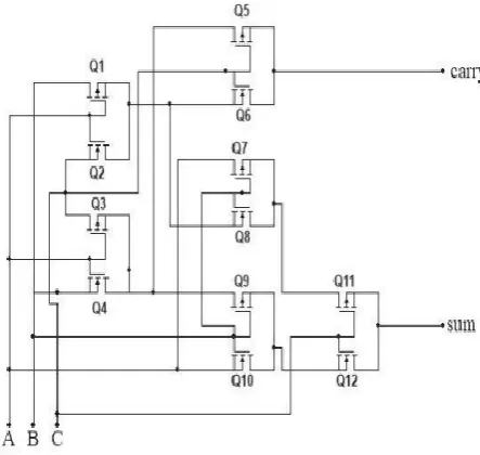
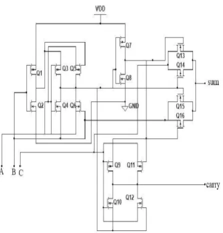
Figure 4. Gated design for Adder Circuits
Figure 5. Schematic for SERF Adder
Figure 6. 14T transistor Adder circuit
Figure 7. Pseudo nMOS Adder Circuit
Figure 8. Multiplexer based Adder circuit design
Figure 10. Inverter and Transmission Gate based adder design
Figure 11. Hybrid Adder Circuit Design
III.
RESULTS AND DISCUSSION
A. Comparison of various adders based on their delay analysis and associated process
technologies
The performance analysis of several full adders drawn in table- 1 shows different adders with different parameter values and different technology, no single adder have less delay,. Thus, there exists tradeoff between these parameters. The results are helpful in selection of an adder according to desired result and application.
Table 1. Comparison Table of Various adder circuits on the basic of delays and associated process technologies
Design Name Process Technology
Delay (in ns)
6 Transistor 350 nm 0.133 ns
8 Transistor 150 nm 0.010 ns
9 Transistor 120 nm 0.295 ns
10 Transistor 180 nm 1.057 ns
12 Transistor 350 nm 0.217 ns
14 Transistor 180 nm 0.338 ns
20 Transistor 180 nm 0.250 ns
Pseudo NMOS 180 nm 0.182 ns
CMOS 180 nm 0.127 ns
A kind of activity which uses a computer to assist on the creation, modification and analysis of design. CAD tools generally consist of the following components, input handler (input from mouse or keyboard), data structure and algorithms (in memory), output handler (output to display). CAD environment generally consists of a simulator, design space exploration and design sign off. The front end tools are used for design entry editors, simulation synthesis and timing analysis and test generation tools. The back end tools include floor planning place and route, extraction etc. Editors ,simulators, analyzers and synthesizers together contributes in computer oriented design.
B. VLSI CAD Tools Vs Methodology for Adder Design
of the design technology are tightly coupled and correlated in terms of their impact.
Figure 12. VLSI CAD/EDA vs CMOS Design Methodologies [1]
VLSI Design incorporates both the design methodologies and associated CAD tools because both forms the integral parts and should go hand in hand as they evolve based on the designer’s needs.
IV.
CONCLUSION
With design technology, it would be possible to implement, verify and test the complex integrated circuits like adders which is the basic unit of all arithmetic circuits. It is through design technology that the ideas and objectives of design, circuit and fabrication engineers are transformed into reality and the quality of the design tools and associated methodologies determine the design time, performance, cost and the correctness of the final product chip. The development in the design tools, collaborative design methods, the role of human factors and integration factors in the design technology marks the outline of various design methodologies. This paper explains design quality metrics from a CAD tool perspective and basic comparison of various adder topologies. Various shortcomings of the current designs and methodologies to tackle the VLSI design challenges were discussed and several promising remedies and their implications on design and methodologies are explored.
V.
REFERENCES
[1] Randal E. Bryant, Kwang-TingCheng , Andrew B
Kahang, Kurt Kreutzer, Wojciech Maly,Richard Newton, Lawerance Pileggi, Jan M Rabaey, Alberto Saniovanni- Vincentelli, “Limitations and Challenges of CAD technology for CMOS VLSI”
[2] S. Roy and C. T. Bhunia, “On Synthesis of
Combinational Logic Circuits,” International Journal of Computer Applications, vol. 127,no 1, pp. 21-26, 2015.”
[3] A.H. Farrahi, D.J. Hathaway, M.Wang and
M.Sarrafzadeh, “Quality OF EDA CAD Tools: Definitions, Metrices and Directions”
[4] Anantha Chandrakasan, Isabel Yang, Carlin Veiri,
Dimitri Antoniadis, “Design Considerations and tools for Low voltage Digital system Design”
[5] Mike Spreitzer “Comparing Structurally different
views of a VLSI Design”
[6] Catherine H. Gebotys, Mohamed I. Elmasry,
“VLSI Design Synthesis and Testibility”
[7] T.S. Cheung, K.Asada, K.L. Yip, H. Wong, Y.C.
Cheng, “Low Power CMOS Design
Methodologies with reduced voltage swing ”
[8] K.A. Sumithra Devi, “Algorithms for CAD tools
VLSI design”
[9] Jan M. Rabaey, Anantha Chandrakasan, Borivoje
Nikolic, “Digital Integrated Circuits” , A Design perspective Second edition
[10] Dr. Nicos Bilalis, “Computer Aided Design
CAD”, January 2000 edition
[11] Course: “Trends in VLSI Design: Methodologies
and CAD tools”. Presenter Raj Singh. IC Design group,CEERI,Pilani-333031
[12] P.van der Wolf. “CAD Frameworks: Principle and
Architecture” Kluwer Academic Publishers,236pp
[13] K.Chaudhary, A.Onawaza, and E.S. Kuh.
“Algorithms for Performance Enhancement and Crosstalk Reduction”. In International conference on Computer Aided Design, pages 697-702,1993.
[14] C.Chen and M.Sarrafzadeh. “Provably Good