Analysis of Structural Stress in InSb Array
Detector without Underfill
Qingduan Meng
Henan University of Science and Technology/School of Electronic Information Engineering, Luoyang, China Email: [email protected]
Xiaoling Zhang and Liwen Zhang
Henan University of Science and Technology/College of Electronics and Information Engineering, Luoyang, China Email: {sunnyzhangxl, zlwshm}@163.com
Abstract—Hybrid infrared focal plane arrays (IRFPAs) are more and more used in both infrared medium and long wavebands for many different applications. In order to offer more spatial resolution, larger format (2048×2048) start to be available, yet its final yield is so low that its cost is very high, and is not affordable. In this paper, basing on viscoplastic Anand’s model, the structural stress of indium antimonide (InSb) infrared focal plane arrays detector without underfill dependent on both indium bump sizes and array formats is systematically researched by finite element method. For shortening simulation time, three-step method is employed to research Von Mises stress and its distribution in InSb infrared focal plane arrays. First, the structural stress of 8×8 InSb infrared focal plane arrays detector is systematically analyzed by finite element method, and the impacts of design structural parameters including indium bump diameters, heights and InSb chip thicknesses on both Von Mises stress and its distribution are discussed in this manuscript. Simulation results show that as the diameters of indium bump decreases from 36µm to 24µm in step of 2µm, the maximum stress existing in InSb chip firstly reduces, then increases linearly with reduced indium bump diameters, and reaches minimum with indium bump diameter 30µm, the stress distribution at the contacts areas is uniform and concentrated. Furthermore, it seems that the varied tendency has nothing to do with indium bump standoff height. With indium bump diameter 30 µm, as the thickness of InSb chip reduces from 21µm to 9µm in step of 3µm, the varying tendency of the maximum stress value in InSb chip is just like the letter U, as the indium bump thickness decreases also from 21µm to 6µm in step of 3µm, the maximum stress in 8×8 InSb IRPFAs decreases from 260MPa to 102MPa, which is the smallest Von Mises stress value obtained with the indium diameter 30µm, thickness 9µm and InSb thickness 12µm. Basing on the above simulated results, a typical InSb infrared focal plane arrays structure with indium bump diameter 30µm, standoff height 20µm and InSb thickness 10µm is selected, then, InSb IRFPAs array format is doubled once again from 8×8 to 64×64 to learn the effect from array size, thus, the Von Mises stress and its distribution of 64×64 InSb IRFPA is obtained in a short time. Simulation results show that Von Mises stress maximum in InSb chip and Si readout
integrated circuit almost do not increases with array scale, and the largest Von Mises stress is located in InSb chips. Besides, stress distribution on the bottom surface of InSb chip is radiating, and decreases from core to four corners, and stress value at contacting area is smaller than those on its surrounding areas, contrary to stress distribution on top surface of InSb chip. Finally, employing the relative displacement theory produced by thermal cycles between InSb detector and silicon readout integrated circuit, an equivalent method is proposed to simulate the relationship between the structure stress of large format InSb infrared focal plane arrays versus array format. The simulated results show that as array format is enlarged from 32×32 to 256×256, the maximal Von Mises appearing in InSb chip fluctuates at 280MPa, simultaneously, the site at which the maximal Von Mises appearing in InSb chip is fixed at the diagonal line of indium bump array with the distance of 5 indium bumps. When the array format is over than 384×384, the maximal Von Mises increases linearly from 326MPa to 1090MPa, which is the maximal Von Mises appearing in InSb chip with format 1024×1024, here the site at which the maximal Von Mises appearing in InSb chip is also fixed at the diagonal line of indium bump array with the distance of 10 indium bumps.
Index Terms—Infrared focal plane array, structural stress, finite element method, stress concentration
I. INTRODUCTION
Indium antimonide (InSb) pn junctions are widely used as infrared photovoltaic detectors and imaging sensors for the 3-5 µm spectral range [1, 2]. For higher spatial resolution of the image, InSb staring infrared focal plane arrays (IRFPAs) detector is commonly designed with larger formats, such as 1024×1024 pixels (1024 columns, 1024 rows), and 2048×2048 or even more larger arrays [3-5]. InSb IRFPAs is usually fabricated by flip chip bonding technology, that is, indium bumps are formed firstly on both detector arrays and Si readout integrated circuits (ROIC), then the detector arrays and Si ROIC are aligned and force is applied to cause indium bumps to cold-weld together, after that underfill is dispensed between InSb die and Si ROIC substrate for increasing the reliability of flip-chip packaging. In order to obtain
Manuscript received March 20, 2011; revised June 1, 2011; accepted July 1, 2011.
higher signal to noise ratio, InSb IRFPAs usually operate at liquid nitrogen temperature (77K), yet stored at room temperature (300K), when its temperature rapidly reduces from 300K to 77K, due to thermal mismatch of the different coefficients of thermal expansion (CTE) of neighboring components, the induced thermal strain and stress are the major causes of fracture in InSb chip, especially in larger format infrared focal plane arrays, which limits the final yield. To reduce the number of InSb chip fracture during rapid temperature dropping, it is necessary to analyze the induced thermal strain and stress values and its distribution in InSb chip.
At present time, various techniques have been developed for the prediction and assessment of long-term reliability of flip chip device. Among them, the low cycle fatigue testing and numerical simulation techniques are two widely accepted methods. In low cycle fatigue testing [6-9], the commonly used techniques are the actual in situ deformation testing of the solder joints. The measured thermal deformation was then substituted into fatigue models, which enabled the fatigue lives of the packages to be predicted. But they tend to be very expensive and time-consuming. In numerical simulation [10-12], statics-based numerical methodologies such as finite element method (FEM) modeling are applied for reliability prediction. Yet as the format of infrared focal plane arrays increases, the meshing number of IRFPAs model increases sharply, which usually makes FEM program operate more slowly [13], for example, to calculate the structural stress of an infrared focal plane array with meshing number over one million, operated on a workstation with two CPUs and 8G memory, its solving time last 21days, so only the small format flip chip device are assessed by this method.
It is well known that the displacement indium bumps experience during thermal cycles is proportional to the distance from the indium joint to the center point of FPAs hybrid, the CTE mismatch between silicon readout integrated circuit and InSb chip and temperature change [14]. Thus when the format of infrared focal plane arrays increases, its side is enlarged, according the equivalent principle, the side elongation can be replaced by increasing thermal mismatch existing between silicon ROIC and InSb chip, at the same time, keeping the product of both the distance from the indium joint to the center point of FPAs hybrid and the thermal mismatch between silicon ROIC and InSb chip unchangeable. This is the modified method proposed in this manuscript, which is used to simulate the structural stress of larger format infrared focal plane array.
Indium is commonly used as an attachment material in packaging structures intended for operation at extreme cold-temperature environment applications for its excellent wetting characteristics, greater ductility, and excellent conductivity at cryogenic temperatures [15-17]. Indium remains very ductile even at cryogenic temperatures (e.g., 196℃). The deformation behavior in thermal fatigue is associated with the irreversible, temperature- and rate-dependent inelastic characteristics, which are known to be viscoplastic. In particular, indium
has been shown to exhibit creep and stress relaxation-dominated deformation behavior at its high homologous temperature as low as 15℃. In 2009, Ruiwu Chang research group delivers the constitutive relations of indium in extreme-temperature in Anand’s model [18-20], a rate and temperature dependent constitutive model, applied to represent the inelastic deformation behavior of indium at low temperatures down to -150℃. Based on the above research results, firstly, the structural stress of 8×8 InSb array detector without underfill dependent on both indium bump sizes and InSb thickness is systemically researched by finite element method. Then basing on the above simulated result, the sizes of InSb IRFPAs is doubled once again to learn the stress value varying tendency with array scale, thus, the stress and its distribution of 64×64 InSb IRFPAs is obtained in a short time. In order to learn the relationship between the structure stress of larger format InSb IRFPAs versus array format, the equivalent method proposed in this paper is used to simulate the structural stress of large format infrared focal plane array.
II. MODEL CREATION AND PARAMETERS SELECTION
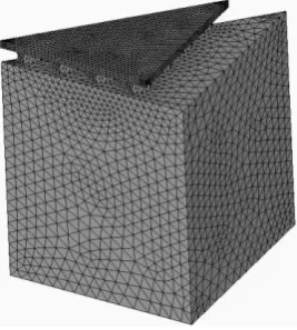
When creating the finite element analysis model of InSb IRFPAs detector, indium bumps are assumed to be octagonal prisms, and no defects existing in the whole device. InSb IRPFAs is composed of InSb photodiodes array, indium bumps array and Si ROIC, just as shown in Fig. 1. InSb chip dimensions are 400μm×400μm ×9~21μm, and attached to the Si ROIC substrate with 8×8 indium bumps array, Si ROIC substrate dimensions are 500μm×500μm×300μm, indium bump has diameter range of 24~36μm with 50μm pitch, and its height increases from 6μm to 21μm in step of 6μm. Using the geometrical symmetry, only one eighth of the overall package is modeled. One eighth models contain 6 full and 4 half indium bumps.
Figure 1. Three dimensional model of infrared focal plane arrays.
InSb IFFPAs finite element analysis model is created by top down method, that is, model is made up of block volume, then Booleans operation is used to divide the block, after that the glue command realizes the contacts between any neighboring components.
parameters listed in table 1, E is the Young’s modulus, µ is the Poisson’s ratio, and CTE is the coefficient of thermal expansion. Flip chip process is completed at 370 K, at this temperature, no residual stress is assumed to exist within the whole package. In the simulation, the temperature is gradually reduced from 370K to 77K, which causes thermal stresses to develop. Throughout the temperature drop, no transient heat transfer is considered and the temperature within the model is assumed to be uniform. About 71 seconds time increments are taken to lower the temperature to ensure the accuracy. Horizontal displacements normal to the symmetrical surfaces are set to zero, at the same time; the bottom surface center point of the Si ROIC substrate also remains zero to avoid body motion.
TABLE I.
LINER ELASTIC MATERIAL PARAMETERS
Materials
Elastic modulus (E/MPa)
Poison’s ratio (µ)
CTE
(αl ppm/K)
Si ROIC 163000 0.28 2.50
InSb chip 409000 0.35 5.04
Indium bump 10600 0.45 33.00
Indium bump deformation is strongly temperature and time dependent, and associated with the irreversible, temperature and rate dependent inelastic characteristics, which are known to be viscoplastic. Here Anand’s viscoplastic constitutive model has been used to describe mechanics of constitutive relationship of indium bump. Within the framework of this model, there appears a scalar-valued function for the equivalent plastic strain rate and an evolution equation for the internal variable. Based on the compression test data, the material parameters of indium bump in Anand’s model were determined to simulate the steady-state viscoplastic behavior and stress/strain responses [18]. The model accommodates the strain rate dependence on the stress using the following expression
m p
s RT
Q A
1
)] )[sinh(
exp(
, (1)
where p is the inelastic strain rate, A is the
pre-exponential factor, Q is the activation energy, R is universal gas constant, T is absolute temperature, m is strain rate sensitivity of stress, ξ is multiplier of stress, s is coefficient for deformation resistance saturation value, and σ is stress. The evolution equation for the internal variable s, which includes the three mechanisms of strain hardening, dynamic recovery, and static recovery, is derived as follows
1 , )} 1 ( 1
{ 0 * *
a
s s sign s
s h
s p
a
, (2)
n p
RT Q A
s
s*[ exp( )] , (3)
where h0 is hardening/softening constant, α is strain rate
sensitivity of hardening or softening, s* is the saturation value of s, ŝ is the coefficient, and n is the strain-rate sensitivity for the saturation value of deformation resistance. There are nine material parameters in the Anand’s model, A, Q, ξ, m, h0, ŝ, n, a and s0, with the last
being the initial value of the deformation resistance. As shown in table 2.
TABLE II.
MATERIAL PARAMETERS OF INDIUM FOR STEADY-STATE PLASTIC
FLOW
Material parameters Values
A (1/s) 2.33×10⁸
Q/R (1/K) 9369.7
ζ 49.97
m 0.30
ŝ (N/m2) 2.83×10⁷
n 0
h0 0
a 1
s0 (N/m2) 2.83×10⁷
III. SIMULATION RESULTS ANALYSIS
A. 8×8 InSb IRFPAs
When temperature of InSb IRFPAs is gradually reduced from 370K to 77K in 10 seconds, Von Mises stress distribution of indium bumps is illustrated in Fig. 2. For those indium bumps locating on diagonal, Von Mises stress on the contacting areas is apparently concentrated and larger. Compared with non-diagonal sites indium bumps, indium bumps situated on diagonal have the larger distance to neutral point (DNP) on the chip, so have larger induced thermal stress. Yet the maximal Von Mises stress appears on the contact area between indium bumps and InSb chip, which is the farthest away from the neutral point, this is different from conventional PbSn solder joints flip chip device, where the maximal stress appears at the biggest coefficient of thermal expansion mismatch existing in two neighboring materials. The maximal stress location changes from indium bump bottom surface to top surface is attributed to thinner thickness InSb chip (10µm) is used, as the InSb chip became thinner and thinner by chemical mechanical polishing method, its anti-deformation intensity changes smaller and smaller, thus the Von Mises stress will redistribute among the whole device, the final stress distribution means the smallest system energy.
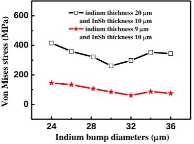
Fig.3. When indium bump height is fixed 20µm, the maximal Von Mises stress in the InSb chip reduces firstly from 344MPa to 261MPa, increases then linearly to 415MPa with reduced indium bump diameters. When indium bump height is fixed 10µm, the maximal Von Mises stress in the InSb chip has the same varied tendency, just like indium bump height with 20µm, that is, reduces firstly from 75MPa to 61MPa, then, increases to 146MPa. The only difference is that the stress value is smaller, and the varied amplitude is also smaller. It is worth noticing that when the diameter of the indium bump is set to 30µm, the maximum stresses in InSb chip reaches the minimum, and the stress distribution at the contacts areas is uniform and concentrated, this phenomena has nothing to do with indium standoff height. So when researching the relationship of stresses in InSb chip dependent on indium bump height and InSb thickness, the indium bump diameter is set to 30µm.
Figure 2. Von Mises stress distribution of 3-D indium bump array.
24 28 32 36
0 200 400
600 indium thichness 20 m
and InSb thickness 10 m
indium thichness 9 m
and InSb thickness 10 m
Indium bump diameters (m)
Von Mises st
re
ss (M
Pa)
Figure 3. Von Mises stress maximum values of InSb chips as a function of indium bump diameters.
In order to learn the effect from the indium bump height and InSb chip thickness on Von Mises stress value and distribution in InSb chip, here the height of indium bump reduces from 21µm to 6µm in step of 3µm, and InSb chip thickness decreases from 21µm to 9µm also in step of 3µm. For any structure, model meshing, constraints, loading are identical for comparison of
simulation results, just as shown in Fig. 4. For a fixed indium height, as the InSb chip thickness reduces from 21µm to 9µm, Von Mises stress maximum values of InSb chip follows a non-monotonic trend, this indicates that for this specific architecture, the optimum levels of these parameters are in the selected range. The total varying tendency is just like the letter U, the minimal value exists with some specific sizes. For fixed InSb chip thickness, as the indium height reduces from 21µm to 6µm in step of 3µm, the maximum Von Mises stress values of InSb chip increases firstly, then decreases, later on increases again, reaches minimal value as indium bump height is 9µm, about one third of maximal value with 18µm indium bump height. So indium bump height has a remarkable effect on maximal stress value than InSb chip thickness.
9 12 15 18 21
100 200 300 400 500
In height 21 m
In height 18 m
In height 15 m
In height 12 m
In height 9 m
In height 6 m
Von Mises str
ess (
M
Pa)
Thickness of InSb (m)
Figure 4. Von Mises stress maximum values of InSb chip as a function of InSb thickness with varied indium bump standoff height.
Figure 5. Von Mises stress distribution of InSb chip bottom surface.
value is about 40MPa, and the stress existing on non-contact areas fluctuate around 15MPa. There is an obvious stress gradient from contact section to non-contact region, and the stress value of non-contact areas along diagonal are larger than other’s. Von Mises stress existing on contact areas between Si ROIC and indium bump also shows concentrated and uniform, its value is also about 40MPa, and the stress existing on non-contact areas is negligible, as shown in Fig. 6 [21].
Figure 6. Von Mises stress distribution of Si-CMOS readout integrated circuit.
B. 64×64 InSb IRFPAs
Usually the indium solder bump with higher standoff height provides better reliability life cycles. In this paper, for obtaining the Von Mises stress value and its distribution in 64×64 InSb IRFPAs in short time period, a typical structure with indium bump diameter 30µm, thickness 20µm and InSb thickness 10µm, is selected. As the indium bump number in row and column increases from 8 to 64 in step of double, that means the InSb IRFPAs scale increases from 8×8 to 16×16, 32×32 and 64×64, here InSb chip is meshed with smart meshing, then refined with one level, the edge length of indium bump is divided by one and the height of indium bump is divided by two, and Si ROIC is also meshed with smart meshing. Simulation results are shown in Fig. 7. Apparently, Von Mises stress maximum in both InSb chip and Si ROIC almost keep constant, and do not vary greatly with increased indium bump array scale, besides, Von Mises stress difference between them is also invariable, which seem to have nothing to do with array scale. And stress in InSb chips is larger than that in Si ROIC, which means that the largest Von Mises stress is located in InSb chips.
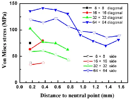
In order to learn the Von Mises stress dependence of indium bump locations, here some typical sites are selected, one group is located in the diagonal of the square array, the other is situated in the middle column or row array parallel to the sides of the array square, their spacing are 0.28mm and 0.20mm, respectively. Simulation results are illustrated in Fig. 8 and Fig. 9. Apparently, for those sites far away from the neutral point in the diagonal of any array scales, their stress
values (about 80MPa) are almost at the same level, but for the sites with 0.16 mm distance to neutral point, as the detector array scale increases from 8×8 to 64×64, its Von Mises stress increases from 75 to 63, 103, 136MPa, for larger array scales, it seem that the adjacent stress value difference is almost fixed at 35MPa. For the 64×64 InSb IRFPAs, when the sites change from neutral point to four corners, its Von Mises stress varying tendency is just like letter Z, firstly fluctuates at 140MPa, then decreases sharply to 80MPa and later on keeps invariable.
8 16 24 32 40 48 56 64
0 50 100 150 200 250
Numbers of indium bump in row and column InSb
Si
Von Mises st
re
ss (M
Pa)
Figure 7. Von Mises stress value of InSb chip VS numbers of indium bump in row and column.
Figure 8. Von Mises stress value of InSb chip VS distance to neutral point for sites in diagonal.
which is vertical to the InSb chip surface, here the displacements in Z direction for the sites situating in the middle row array change from -0.64μm to -0.19μm, which means the whole InSb chip moves downward with temperature dropped to 77K, but for those sites near the neutral point, whose displacements are larger than those sites far away from the neutral point, thus the inner parts of the InSb chip is compressed larger than the outer part, correspondingly Von Mises stress in inner part is larger than that in outer part. For those sites at diagonal, whose displacements in Z direction increase from -0.66μm to 0.27μm, which means, for those sites near the neutral point, which move downward, yet for those sites far away from the neutral point, which shift upward. Thus in the core of the array the structure is compressed greatly and at the corners of the array the structure is stretched slightly, so the stress distribution is radiating, and the stress values decrease from inner to outer region. For the 64×64 InSb infrared focal plane array, Von Mises stress values in diagonal fluctuate at 105MPa with amplitude of 35MPa, and Von Mises stress values in middle row fluctuate at 100MPa with amplitude of 20MPa. On the whole, the stress distribution is uniform and favorable to avoiding InSb cracking.
Figure 9. Von Mises stress distribution of InSb chip top surface with 64 × 64 arrays.
Figure 10. Von Mises stress distribution of InSb chip bottom surface with 64 × 64 arrays.
Fig. 9 and Fig. 10 are Von Mises stress distribution of InSb chip top surface and bottom surface with 64×64 arrays, respectively. Apparently in the core of the 64×64 array, the Von Mises stress is larger, and at the four corners, the stress is smallest, and stress distribution is radiating, decreases from core to four corners. Furthermore, Von Mises stresses at InSb chip top surface, over the contacting areas between InSb chip and indium bump arrays, is larger than its surrounding zone, this is contrary to InSb chip bottom surface stress distribution, here the stress on contacting areas is smaller than its surrounding areas. This phenomenon originates from the contacted areas which are glued together [22].
Von Mises stress existing on contact areas between Si ROIC and indium bump is shown in Fig. 11. Apparently the stress on the contacting areas is concentrated and uniform, its value is about 30MPa. There is an obvious stress gradient from contact section to non-contact region, and the stress value of contact areas along diagonal are larger than other’s. It is noticed that although the contacting areas between indium bump arrays and Si ROIC are completely identical, yet on the Si ROIC top surface center, its Von Mises stress distribution region is obviously larger than that on the four corners. Just like Von Mises stress distribution on the InSb surfaces, the stress appears radiating and decreases from the core to the four corners.
Figure 11. Von Mises stress distribution of Si ROIC top surface with 64 × 64 arrays.
C. Larger Format InSb IRFPAs
Due to the CTE mismatch between InSb chip and Si substrate, indium bumps for most IRFPAs experience stress from the thermal cycling between 300K and 77K that occurs during normal detector operation. These thermal cycles produce relative displacement between the InSb chip and the Si ROIC resulting in shear stress at the interfaces between the indium bumps and metal pads. The displacement indium bumps experience during thermal cycles is represented as
T
L
L
FPA
Si
where L0 is the distance from the indium joint to the center point of FPAs hybrid, which we can treat as a neutral point where the ROIC and FPA substrate do not contract relative to each other.
FPA and
si are the CTE of the FPA substrate and Si, respectively. T is the temperature change. The shear stress produced by this displacement is represented as:solder Si FPA
h
T
L
0(
-
)
, (5)where is the tangential displacement of indium joint,
which is L per unit joint height hsolder. Apparently both
the displacement and the shear stress indium bumps experience during thermal cycles is proportional to L, the CTE mismatch between silicon readout integrated circuit and InSb chip and temperature change. Usually when the format of infrared focal plane arrays increases twice, according to (4) and (5), both the displacement and the shear stress indium bumps experience is also enlarged twice over. In order to achieve the identical displacement and the shear stress indium bumps experience during thermal shock from room temperature to 77K, a modified method is proposed in this manuscript, which is used to simulate the structural stress of large format IRFPAs without increasing meshing numbers. Here a small format FPAs is used to replace the larger format FPAs to simulate the structural stress existing in larger format FPAs, that is, the thermal mismatch existing between silicon readout integrated circuit and InSb chip is increased twice, and fixing the side length of FPAs. According to (4) and (5), both the displacement and the shear stress indium bumps experience in this method are also enlarged twice over.
In order to learn the relationship of Von Mises stress in InSb chip dependent on the format of InSb IRFPAs, here a small format FPAs (32×32) is selected for time and memory saving. When the array format is enlarged from 32×32 to 256×256, the maximal Von Mises appearing in InSb chip fluctuates at 260MPa, simultaneously, the site at which the maximal Von Mises appearing in InSb chip is fixed at the diagonal line of indium bump array with the distance of 5 indium bumps. When the array format is over than 384×384, the maximal Von Mises increases linearly from 326MPa to 1090MPa, which is the maximal Von Mises appearing in InSb chip with format of 1024×1024, here the site at which the maximal Von Mises appearing in InSb chip is also fixed at the diagonal line of indium bump array with the distance of 10 indium bumps. Just as shown in Fig. 12 and Fig. 13. Compared with the simulated results in Fig. 7, where the format of InSb IRFPAs increases from 8×8 to 16×16, 32×32 and 64×64, the Von Mises stress maximum in InSb chip increases gradually from 180MPa to 200Mpa, and do not vary greatly with increased indium bump array scale, below the format 256×256, the relationship of Von Mises stress in InSb chip dependent on the format of InSb IRFPAs, obtained by employing the modified equivalent method, is almost identical with that appears in Fig. 7. This means that the proposed method is available and
accurate in a certain range. Obviously the indium bump with diameter 30µm and height 20µm has the capability of standing the displacement during thermal shock from 300K to 77K with the FPAs format less than 256×256, when the array format is over than 384×384, the thermal mismatch is so large that it can not be absorbed through indium bump distortion, so the location of maximal Von Mises stress in InSb chip changes from the fifth indium bumps to the center point of FPAs hybrid to the tenth indium bumps along the diagonal line of indium bump array, besides, its Von Mises stress increases linearly with FPAs format.
Figure 12. Von Mises stress value of InSb chip VS numbers of indium bump in row and column with 32× 32 equivalent method.
Figure 13. Location of maximal Von Mises stress in InSb chip VS numbers of indium bump in row and column with 32× 32 equivalent
method.
Figure 14. Von Mises stress distribution of InSb chip with format 32× 32.
Figure 15. Von Mises stress distribution of InSb chip with format 384×384 simulated by 32× 32 equivalent method.
Figure 16. Von Mises stress distribution of InSb chip with format 768×768 simulated by 32× 32 equivalent method.
the stress is obviously larger than others region. When the FPAs format is set with 384×384, the Von Mises stress distribution is intervenient between 32×32 and 768×768. It should be noted that the optimal allocation of thermal stress obtained in a small format arrays, such as 8×8, can
not be used in larger format arrays, such as 384×384 and 768×768. As the FPAs format increases, the Von Mises stress uniformed distribution disappears, and along the diagonal of the array, the Von Mises stress becomes much larger and more concentrated, and at others region, the Von Mises stress is reduced to a small level. It should be also pointed out that the optimal allocation of thermal stress obtained in a small format arrays, such as 8×8, can be used to predicate the Von Mises stress distribution of InSb chip with format arrays below 256×256, in this format arrays range, the indium bump arrays can withstand the displacement, caused by the larger CTE mismatch between InSb die and Si ROIC. And the location of maximal Von Mises stress in InSb chip does not change.
Ⅳ. CONCLUSIONS
REFERENCES
[1] Y. Gau, L. Dai, S. Yang, S. Yang, P. Weng, K. Huang, et al, “256×256 InSb focal plane arrays,” Proceedings of SPIE, vol. 4078, pp. 467-479, 2003.
[2] W. Parrish, J. Blackwell, G. Kincaid, and R. Paulson, “Low-cost high performance inSb 256×256 infrared camera”, Proceedings of SPIE, vol. 1540, pp. 274-284, 1991.
[3] A. W. Hoffman, C. Elizabeth, J. L. Peter, J. Rosbecka, M. Michael, A. Fowler, et al, “2K×2K InSb for astronomy”,
Proceedings of SPIE, vol. 5499, pp. 59-67, 2004.
[4] A. Rogalski, “Infrared detectors: status and trends”, Prog. Quant. Electron., vol. 27, pp. 59-210, 2003.
[5] A. W. Hoffman, J. L. Peter, and P. R. Joseph, “Mega-pixel detector arrays: visible to 28 µm”, Proceedings of SPIE
vol.5167, pp. 194-203, 2004.
[6] X. Q. Shi, H. L. J. Pang, W. Zhou and Z. P. Wang. “Low cycle fatigue analysis of temperature and frequency effect in eutectic solder alloy”, Int J Fatigue, vol. 22, pp. 217-228, 2000.
[7] R. Ghaffarian, N. P. Kim, “Reliability and failure analyses of thermally cycled ball grid array assemblies”, IEEE T Compon Pack T, vol.23(3), pp. 528-534, 2000.
[8] J. H. L. Pang, D. Y. R. Chong and T. H. Low. “Thermal cycling analysis of flip chip solder joint reliability”, IEEE T Compon Pack T, Vol. 24, pp. 705-712, 2001.
[9] C. Kanchanomai, Y. Miyashita and Y. Mutoh. “Low cycle fatigue behavior of Sn–Ag, Sn–Ag–Cu and Sn–Ag–Cu–Bi lead-free solders”, J Electron Mater, vol. 31(5), 456-465, 2002.
[10]B. Z. Hong. “Finite element modelling of thermal fatigue and damage of solder joints in a ceramic ball grid array package”, J Electron Mater, vol. 26(7), pp. 814–820, 1997. [11]J. Pang and D. Chong, “Flip chip on board solder joint reliability analysis using 2-D and 3-D FEA models”, IEEE T. Adv. Packaging, vol. 24, pp. 499-506, 2001.
[12]Z. Zhang and C. P. Wong, “Recent advances in flip-chip underfill: materials, process, and reliability”, IEEE T. Adv. Packaging, vol. 27, pp. 515-523, 2004.
[13]Q. Meng, X. Zhang, X. Zhang and W. Sun, “Finite element analysis on structural stress of 64×64 InSb infrared focal plane array”, Appl. Mech. Mater., vols.34-35, 212-216, 2010.
[14]J. Jiang, S. Tsao, T. O’Sullivan, M. Razeghi and G. J. Brown, “Fabrication of indium bumps for hybrid infrared focal plane array applications”, Infrared Phys. Techn.
vol.45, pp. 143-151, 2004.
[15]S. Kim and H. Ledbetter, “Low-temperature elastic coefficients of polycrystalline indium”, Mater. Sci. Eng., A, vol. 252, pp.139-143, 1998.
[16]E. Hermida, D. Melo, J. Aguiar and D. Lopez, “Temperature dependence of the viscoelastic response of In, Sn and In-Sn alloys”, J. Alloys Compd., vol. 310, pp. 91-96, 2000.
[17]R. Reed, C. McCowan and R. Walsh, “Tensile strength and ductility of indium”, Mater. Sci. Eng., vol. 102, pp. 227-236, 1988.
[18]R. Chang and F. Patrick Mccluskey, “Constitutive relations of indium in extreme temperature electronic packaging based on Anand model”, J. Electron. Mater., vol. 38, pp.1855-1859, 2009.
[19]G. Wang, Z. Cheng, K. Becker and J. Wilde, “Applying Anand model to represent the viscoplastic deformation behavior of solder alloys”, J. Electron. Packaging, vol. 123, pp.247-253, 2001.
[20]J. Wilde, K. Becker, M.Thoben, W. Blum, T.Jupitz, G. Wang and Z. Cheng, “Rate dependent constitutive relations based on Anand model for 92.5Pb5Sn2.5Ag solder”, IEEE T. Adv. Packaging, vol. 23, pp.408-414, 2000.
[21]Q. Meng, X. Zhang, X. Zhang and W. Sun, “Finite element analysis on structural stress of 8×8 InSb infrared focal plane array”, Appl. Mech. Mater. vol. 33-34, pp.207-211, 2010.
[22]Q. Meng, Q. Lin, X. Zhang, W. Sun, “Finite element analysis on structural stress of large format InSb infrared focal plane array”, Adv. Mater. Res., vols.152-153, pp. 1721-1725, 2011
Qing-Duan Meng was born in Henan Province, China, in 1978. He received the B.S. degree in applied physics in 2000 and the M.S. degree in microelectronics and solid-state electronics in 2003 from Dalian University of Science and Technology, and the Ph.D. degree in condensed matter physics from Institute of Physics, Chinese Academy of Sciences (CAS), in 2006. His research interests are the design and fabrication of high temperature superconductor (HTS) filters, tunable ferroelectric devices, infrared (IR) detectors.
He is currently an Associate Professor in the College of Electronics and Information Engineering, Henan University of Science and Technology. From 2008 to 2010, he was with the School of Physics and Optoelectronic Technology, Dalian University of Science and Technology, majoring in modeling and simulation in advanced packaging development.
Xiao-Ling Zhang was born in Henan Province, China, in 1977. She received the B.S. degree in computer software from Zhengzhou University in 2000 and the M.S. degree in applied computer technology from Henan University of Science and Technology in 2008. Her research interests include pattern recognition, tunable devices simulation and IR detectors structural optimization.