Optimization of Power and Delay in Nonlinear
Interconnects by using Schmitt Trigger
M. Jayanthi S. Hemalatha
Assistant Professor Assistant Professor
Department of Computer Science & Engineering Department of Computer Science & Engineering PSNA College of Engineering & Technology, Dindigul PSNA College of Engineering & Technology, Dindigul
Abstract
Interconnect delay and power is a primary criterion in design of an Integrated Circuit due to its close relationship to the speed of IC. Interconnect Buffers in very large scale integration (VLSI) circuits is most common method used to reduce power and delay but they result in high Delay and power dissipation, thereby degrading the performance (i.e.) operating speed of an integrated circuit. Use of buffers in interconnect is mainly for optimizing power dissipation and delay in interconnect, but Buffers themselves have certain switching time that contributes to crosstalk delay and power dissipation. For efficiently minimizing both delay and power dissipation in long interconnects is done by replacing buffers with Schmitt Trigger in the Nonlinear Interconnect. since Schmitt trigger have low threshold voltage, Schmitt trigger allows the reduction in rise time and hence saves in terms of total delay. The proposed Schmitt trigger have larger band gap so it reduces the noise compare to that buffer. Keywords: Schmitt Trigger, Buffer, Interconnect, VLSI, DSM
________________________________________________________________________________________________________
I. INTRODUCTION
In deep submicron (DSM) technologies, interconnects no longer behave as Resistors but may have associated parasitic such as capacitance and inductance. With a linear increase in interconnect length, both the interconnect capacitance (C) and interconnect resistance (R) increase linearly, making the RC delay increase quadratic ally. Although the RC delay is not a precise measure of the time necessary for a signal to propagate through a wire, the total RC delay of a section of a line may be useful as a figure of merit. In order to increase the operating speed of an integrated circuit, it is necessary to reduce the RC delay. In addition to increased signal propagation delay, increased power dissipation is another effect of large interconnects impedance. Buffer insertion is becoming a bulky technique for DSM technologies to reduce interconnect delay, requiring to find the solution with different approach. The objective of the project is to develop an alternative approach to buffer Insertion for the purpose of delay, power and noise reduction in VLSI interconnect in DSM technology.
Delay and noise are two equivalent factors in DSM technology. For the purpose of signal restoration and to handle the on-chip delay and noise, buffer insertion technique has been modified and Schmitt trigger is used to replace it in VLSI interconnects at all the possible nodes. In Schmitt trigger, the threshold voltage of the device can be adjusted, so if it is set to low then it can get an early rise in rising signals and hence less propagation delay.
Buffer insertion technique is to find where to insert buffers in the interconnect so that the timing requirements are met. Since the propagation (Elmore) delay has a square dependence on the length of an RC interconnects line, subdividing the line into shorter sections is an effective strategy to reduce the total propagation delay [2].
Owing to the tremendous drop in VLSI feature size, a huge number of buffers are needed for achieving timing objectives for interconnects. It is stated in a recent study [3] that the number of nets that need buffer insertion and the number of buffers will rise dramatically as shown in figure 1
Need for Better Approach
Buffer Insertion is a very effective approach for delay reduction. But as is clear from the above section, in every new generation deep submicron technology, buffer insertion is becoming a major problem, because of their number and also because they now a major source of power dissipation. Hence a trade-off is required between delay and power consumed. Thus there is a need for a new approach that while reducing the delay, also consumes less power.
One of the major limitations of buffer insertion is the increasing number of repeaters in system. As it is shown in figure 1 shows the increasing percentage of total buffered nets in every technology node. Similarly figure 1 shows the increase in buffered cell with each next technology. Hence buffers are occupying a major portion of total area in the system. Similarly this shows the exponential increase in area consumed by buffers for Different interconnect length.
All these factors are not in favour of buffer insertion for interconnect modelling. Thus a major breakthrough is needed to handle interconnects. Hence keeping in mind of all the problems being faced and to be coming with buffer insertion, in this paper, an[1] alternate to buffer is proposed for linear Interconnects.
Schmitt Trigger
[1]Schmitt trigger can be adjusted to deal with analog input signals. The main purpose of Schmitt trigger is to restore the shape of digital signals.
Hence this element can replace buffer as far as restoring the signal is concerned. Due to effect of transmission line, there is transformation of digital shape from square to more complex signal. While transmitting signal, it may become noisy.
Schmitt trigger is a comparator with positive feedback, and also have dual threshold voltage what end in hysteresis, which mean between the lower (U1) and upper threshold (U2) of Schmitt trigger the state of output never change. This effect results in stabilization of output.
The main advantage of Schmitt trigger is its noise immunity due to its larger band gap and single input threshold which allows signal to switch rapidly.
Schmitt Trigger can be implemented using 6 CMOS transistors. This implementation ensures more noise reduction and early rise and fall of signal, which causes less propagation delay too. Thus if Buffer is replaced with Schmitt trigger in interconnects, it is expected to achieve more noise, delay and power reduction.
The classic Schmitt trigger is implemented using an op-amp with two resistors to conduct a regenerative feedback. The circuit representation of Schmitt trigger is given below
Fig. 2: Schmitt trigger implementation with comparator.
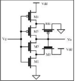
CMOS Schmitt Trigger
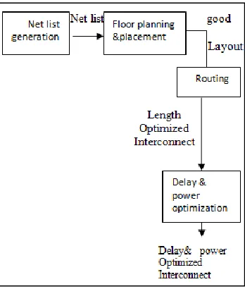
System Architecture
Fig. 4: System Architecture
Netlist Generation
The random circuits are generated. It generates the module sizes, net degree distribution and the nets. It derives the appropriate input parameter values to obtain realistic circuits. The circuits are verified to be without any outliers. This module writes the module sizes and net degree distribution to files.
Certain heuristics that describe a realistic circuit guide us in the net list generation process. Some of them are as follows. There cannot be a few small modules or few very large modules.
The number of pins on a module cannot exceed that it cannot fit within the length of the module. There has to be a good proportion of input and output terminals.
All the pins cannot get accumulated on one side of the module. A single module shouldn’t connect to all the terminals.
Some modules shouldn’t be left unconnected with the rest of the modules.
Now, the pseudo-code for net-degree distribution Ni and Ne for the given number of modules can be written as follows. begin
initialize vectors: Di, De, Ni and Ne;
De(2)=k;(*De distribution for a single module*) H=ceil(log2M);(*Determine the number of iterations*) for h=0 to H-1 do
m1=2h; m2=2h+1; compute PP; update Di and De; end for
for i=2 to M do Ni(i)=round(Di(i)*M); Ne(i)=round(De(i)*M); end for
end
Floor Planning and Placement
Floor planning,[12] which consists of planning and sizing of blocks and interconnect and where as placement assign a specific location to blocks.
The input to the Floor planning phase is a set of blocks, the area of each block, possible shapes of each block and the number of terminals for each block and the netlist.
Routing
Routing is done in order to reduce the interconnect length; there by requirement of placing of number of Schmitt triggers will be less, thus efficiently reduce the delay and power. The main goal of Routing[14] is to complete all circuit connections using the shortest possible wire length. In routing two types i) Global routing ii) Detailed routing. In this project we are focusing on the Global Routing. Global Routing generates a ‘loose' route for each net.
In fact it assigns a list of routing regions to each net without specifying the actual geometric layout of wires. Global routing involves three phases:
Region Definition Region Assignment Pin Assignment
Region Definition
This is to partition the entire routing space into routing regions. Region Assignment:
This is to identify the sequence of regions through which a net will be routed. Pin Assignment:
After the region assignment each net is assigned a pin on region boundaries. This phase allow regions to be independent. After global routing is complete, the output is pin location for each net the all region boundaries it crosses. Using this information we can extract the length of the net. If some net fails to meet its timing budget, global routing needs to be repeated.
Global routing algorithms is of two types a)Sequential approach:
Nets are routed one by one. Ex: shortest path based algorithms, Steiner tree based algorithms b)Concurrent approach:
This approach avoids the ordering problem by considering routing of all nets simultaneously.
Interconnect Delay and Power Optimization
Schmitt trigger as an alternate to buffer to reduce the delay and power, in non linear interconnects. Most favourable feature of Schmitt trigger is its adjustable threshold voltage and it can be controlled, so that threshold voltage can be chosen to be above/below vdd/2 at which buffer normally operate. Schmitt trigger can switch faster than buffer, delay can be reduced greatly by Schmitt trigger compare to that of buffer and since buffer requires more power for switching and refreshing, power dissipation is less by usage of Schmitt trigger. The lower threshold of the Schmitt trigger allows the reduction in rise time and hence saves in terms of total delay. Although the savings in rise time delay are of few ps only, but when we consider slowly rising signals this saving is very significant. With the introduction of Schmitt trigger, all sorts of bus coding techniques can be neglected and thus resulting in reduction of extra hardware and power consumption by those transistors The extra hardware which is required in the form of encoder and decoder for bus coding techniques is also not required. Hence area savings may also be achieved. Output is delay and power optimized non linear interconnects.
Schmitt trigger can act as a signal restoring circuit; this is the main reason why we have looked into the approach of using Schmitt trigger as an alternate of buffer in interconnects as a data restoring element. Reduced noise glitches result in lesser power consumption and hence help in reducing the total power consumed. Noise immunity of Schmitt trigger is more than buffer due to larger band gap.
Interconnect structures used for simulation will be in the form of fig 4
Fig. 5: Interconnect structures used for simulation
Local interconnects are the used to connect the logic blocks, while designing interconnects, width will be kept to be half of the height and thickness of the interconnect. Minimum spacing between two local interconnects is kept to be at least equal to the width of line.
Results
Fig. 6: Results
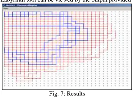
The routing of the nets found by Labyrinth tool can be viewed by the output provided by GUI module is given below
Fig. 7: Results
II. CONCLUSION
We design Nonlinear RC interconnect in that we place buffer, analyse the interconnect behavior under buffer and calculate the delay and power of the interconnect. And later replace the buffer with Schmitt trigger and will calculate the delay and power of Nonlinear RC interconnect and will ensure the use of Schmitt trigger will result in efficient performance such a way that it is optimized in delay and power compare to that of buffer.
REFERENCES
[1] s Annu Khurana, Anshul Saxena, Neeraj Jain (2015)“Evaluation path way of Schmitt Trigger with Leakage Reduction Techniques” ISSN: 2395 -0056 Volume: 02 Issue: 04,pp 1553-1556
[2] Archana Nagda,Rajendra Prasad ,N.K.Vyas,”leakage power reduction techniques:Anew approach”,ISSN 2248-9622,Vol II Issue 2,mar-apr 2012,pp 308-312
[3] Sandeep Saini, A.Mahesh kumar, Sreehari Veeramachaneni(2010), “An Alternative approach to Buffer Insertion for Delay and Power Reduction in VLSI Interconnects,”23rdInternational Conference on VLSI Design,411-416.
[4] P. Saxena and N. Menezes and P. Cocchini and D.A. Kirkpatrick(2004), “Repeater scaling and its impact on CAD”, IEEE Transactions on Computer-Aided Design, vol. 23, no. 4, pp. 451-463.
[5] H. Zhou, D. F. Wong, I. M. Liu, and A. Aziz(2000), “Simultaneous routing and buffer insertion with restrictions on buffer locations”, IEEE Trans. on Computer Aided Design of Integrated Circuits and Systems , vol. 19, no. 7, pp. 819-824.
[6] J. Lillis, C. K. Cheng and T.-T. Y. Lin (1996), “Optimal wire sizing and buffer insertion for low power and a generalized delay model”, IEEE Trans. Solid-State Circuits, vol. 31, no. 3, pp. 437-447.
[7] C. J. Alpert and A. Devgan (1996), “Wire segmenting for improved buffer insertion”, in Proc. ACM/IEEE Design Automation Conf, pp. 588-593. [8] H. B. Bakoglu and J. D. Meindl (1985), “Optimal Interconnection Circuits for VLSI,” IEEE Transactions on Electron Devices, Vol. ED-32, No. 5, pp.
903-909.
[9] S. Yu et al.(2006), “Loop-Based Inductance Extraction and Modeling for Multiconductor On-Chip Interconnects,”IEEE Transactions on Electron Devices, Vol. 53, No. 1, pp. 135-145.
[10] T. Dhaene and D. D. Zutter(1992), “Selection of Lumped Element Models for Coupled Lossy Transmission Lines,” IEEE Transactions on Computer-Aided Design of Integrated Circuits and Systems, Vol. 11, No. 7, pp. 805-815.
[11] M. A. El-Moursy and E. G. Friedman (2003), “Optimum Wire Shaping of an RLC Interconnect,” Proceedings of the IEEE Midwest Symposium on Circuits and Systems.
[12] Sherwani, N.A., (1995), “Algorithms for Physical Design Automation”.2nd Edn. Kluwer Academic Publishers Norwell, MA.USA. ISBN: 0792395921 [13] Yogeshwar Singh Randhawa and Sanjay Sharma, “Effect of Multi Threshold Techniques on Compretive Study of 11T and 6T Cell during Leakage Power