e-ISSN: 2278-067X, p-ISSN: 2278-800X, www.ijerd.com
Volume 9, Issue 2 (November 2013), PP. 22-29
The Computer Architecture of a Microcontroller Based
Transistor Tester with a Logic Display
Aru Okereke Eze
1, Opara, F.K
2.
1Department of Computer Engineering Michael Okpara University of Agriculture, Umudike, Umuahia, Abia
State, Nigeria
2
Department of Electrical/Electronics Engineering Federal University of Technology, Owerri, Imo State, Nigeria
Abstract:- This work exploits the design and implementation of a microcontroller based transistor tester with a logic control. Microcontroller based transistor tester is a device used to test the electrical behaviour of transistors and diode states within transistors. The transistor device is commonly used for circuitry and electronics. Most transistor testers test whether or not a transistor is sinking input(NPN) or sourcing output (PNP). This work is aimed at designing a microcontroller based transistor tester required to test Bipolar Junction Transistor, Field Effect Transistor and Uni-junction Transistor. It is also aimed to experimenting and producing a well reliable transistor, not only testing Bipolar, Field Effect and Uni-junction transistor but also other electronics component useful in daily human lives.
Keyword:- Microncontroller, Transistor Tester, Liquid Crystal Display, Adc0804, Cpu, Rom, Ram, Etc.
I.
INTRODUCTION
A microcontroller is an integrated chip that is often part of an embedded system. The microcontroller includes a CPU, RAM, ROM, I/O ports, and timers like a standard computer, but because they are designed to execute only a single specific task to control a single system, they are much smaller and simplified so that they can include all the functions required on a single chip. Microcontrollers have become common in many areas, and can be found in home appliances, computer equipment, and instrumentation. They are often used in automobiles, and have many industrial uses as well, and have become a central part of industrial robotics and most especially in the design of a transistor testing devices.
Microcontroller based transistor tester is a device used to test the electrical behaviour of transistors and diode states within transistors. The transistor device is commonly used for circuitry and electronics. Most transistor testers test whether or not a transistor is sinking input(NPN) or sourcing output (PNP).
A microcontroller based transistor tester is used to test bipolar junction transistors. It uses a method to type, pin and check for forward direct current (DC) gain. It can be used to test field effect transistor. A FET can be tested using a transistor tester and is needed wherein the correct biasing voltages can be applied and the tester display can reveal the full operating characteristics of the device. And also it can test Unijunction transistor by checking the resistancebetween B1 and B2.
II.
SYSTEM METHODOLOGY
It is noted that the project is Micro-controller based, with some discrete components.
A liquid crystal display (LCD) is a thin, flat panel used for electronically displaying information such as text, images, and moving pictures. Its uses include monitors for computers, televisions, instrument panels, and other devices ranging from aircraft cockpit displays, to every-day consumer devices such as video players, gaming devices, clocks, watches, calculators, and telephones. Among its major features are its lightweight construction, its portability, and its ability to be produced in much larger screen sizes than are practical for the construction of CRT display technology.
In generating the address, they are sent to the memory unit [RAM]) through the address bus of the RAMs. This unit constitutes of 128 x 8-bit internal RAM, since the unit functions as the memory storage unit of the generated addresses, it sends the addresses generated in form of patterns of display through the data bus to the drivers. This pattern of display is achieved by how the Micro-controller is reprogrammed,
3.2 AT89C52 MICROCONTROLLER
The AT89C52 is a low-power, high-performance CMOS 8-bit microcomputer with 8K bytes of Flash programmable and erasable read only memory (PEROM). The device is manufactured using Atmel's high-density non-volatile memory technology and is compatible with the industry-standard 80C51 and 80C52 instruction set and pin out.
The on-chip Flash allows the program memory to be reprogrammed in-system or by a conventional non-volatile memory programmer. By combining a versatile 8-bit CPU with Flash on a monolithic chip, the Atmel AT89C52 is a powerful microcomputer which provides a highly-flexible and cost-effective solution to many embedded control applications.
Features of AT89C52 micro-controller:
8k Bytes of In-System Reprogram-able Flash Memory Endurance: 1,000 write/Erase Cycles
Full Static Operation: 0 HZ to 24 MHZ Three level Program Memory Lock 256x 8-bit Internal RAM
32 Programmable I/O Lines Two 16-bit Timer/Channel Eight interrupt Sources Programmable Serial Channel
Low power Idle and Power-down Modes
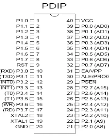
3.3 MICRO-CONTROLLER PIN DESCRIPTIONS ALE/PROG
Pulse is skipped during each access to external Data Memory. If desired, ALE operation can be disabled by setting bit 0 of SFR location 8EH. With the bit set, ALE is active only during a MOVX or MOVC instruction. Otherwise, the pin is weakly pulled high. Setting the ALE-disable bit has no effect if the micro-controller is in external execution mode.
PSEN
Program store Enable is the read strobe to external pro-gram memory. When the AT89C52 is executing code from external program memory, PSEN is activated twice each machine cycle, except that two PSEN activations are skipped during each access to external data memory.
EA/VPP
External Access Enable. EA must be strapped to GND in order to enable the device to fetch code from external program memory locations starting at 000H up to FFFH. Note, however, that if lock bit 1 is programmed, EA will be
Internally latched on reset.
EA should be strapped to V CC for internal program executions. This pin also receives the 12-volt programming enable volt-age (VPP) during Flash programming, for parts require 12-volt VPP. From the diagram, pin 40 is connected to Vcc, while pin 20 is the ground pin. Pin 9 is the reset pin, which must be connected to Vcc through a 10μF capacitor for CMOS version.
XTAL1
Input to the inverting oscillator amplifier and input to the internal clock operating circuit.
XTAL2
Fig 1: Micro-controller pin configuration Port 0
Port 0 is an 8-bit open drain bi-directional I/O port. As an output port, each pin can sink eight TTL inputs. When 1s are written to port 0 pins, the pins can be used as high-impedance inputs.
Port 0 can also be configured to be the multiplexed low-order address/data bus during accesses to external program and data memory. In this mode, P0 has internal pull-ups.
Port 0 also receives the code bytes during Flash programming and outputs the code bytes during program verification. External pull-ups are required during program verification.
Port 1
Port 1 is an 8-bit bi-directional I/O port with internal pull-ups. The Port 1 output buffers can sink/source four TTL inputs. When 1s are written to Port 1 pins, they are pulled high by the internal pull-ups and can be used as inputs. As inputs, Port 1 pins that are externally being pulled low will source current (IIL) because of the internal pull-ups. In addition, P1.0 and P1.1 can be configured to be the timer/counter 2 external count input (P1.0/T2) and the timer/counter 2 trigger input (P1.1/T2EX)..
Port 1 also receives the low-order address bytes during Flash programming and verification.
Port 2
Port 2 is an 8-bit bi-directional I/O port with internal pull-ups. The Port 2 output buffers can sink/source four TTL inputs. When 1s are written to Port 2 pins, they are pulled high by the internal pull-ups and can be used as inputs. As inputs, Port 2 pins that are externally being pulled low will source current (IIL) because of the internal pull-ups. Port 2 emits the high-order address byte during fetches from external program memory and during accesses to external data memory that uses 16-bit addresses (MOVX @ DPTR). In this application, Port 2 uses strong internal pull-ups when emitting 1s. During accesses to external data memory that uses 8-bit addresses (MOVX @ RI), Port 2 emits the contents of the P2 Special Function Register.
Port 2 also receives the high-order address bits and some control signals during Flash programming and verification.
Port 3
P3.6 WR (external data memory write strobe) P3.7 RD (external data memory read strobe)
EA/VPP
External Access Enable. Pin 31 (EA/VPP) must be connected to Vcc only of the microcontroller will use its internal RAM and ROM, otherwise EA must be strapped to GND in order to enable the device to fetch code from external program memory locations starting at 0000H up to FFFFH. Note, however, that if lock bit 1 is programmed, EA will be internally latched on reset.
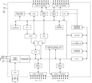
Fig 2: Internal block diagram of Microcontroller AT89C52.
Fig 3: Standard transistor tester block diagram
IV.
SOFTWARE DEVELOPMENT
Software development involves series of steps or is a set of activities that are necessary to be taken for the development of reliable and maintainable software. It is of great importance because hardware design cannot be used in micro-controller based systems without dependable software. A typical micro-controller development systems (MDS) includes; VDU, Registers, RAM, which serves as a store for the PROM programmer.
It also includes programs that facilitate program modification (editor). The computer aided development methodology, which is essential for software development, is summarized below.
TEXT EDITOR:
This is a kind of word processor that is used to in programming. After keying in the program codes using the input device and the program is displayed on the VDU, the Text editor can be used to check and correct errors in the program in the program. In a nutshell, the text editor is used to edit the program after it has been written.
TRANSLATOR
There are two types of translators, assembler and complier. An assembler translates assembly language in the form of mnemonic (memory aids) into machine code. A good feature of assemblers is creating a list that shows the machine code and the assembly language of the program side by side. A complier on the other hand translates a high-level language into machine code.
LINKER/LOCATOR
This is used to join the different modules that make up the program together in the correct sequence and this is to be bound to addresses. The linker/locator pair works together to coordinate between the separate modules for smooth program execution.
LOADER
The loader aids in loading an object code into RAM.
TESTING
After the program is written, it was tested; it was tested; this involves executing the program with selected inputs called test cases, the result of the test is used to decide whether or not the program is functioning as desired.
DEBUGGING
This involves detecting out and removing errors in the program.
V.
DEVELOPMENT PROCESS
In writing the software for this project a modular approach was employed. This made it easier to check for errors and debug the program. The choice of assembly language is because it makes a program small and enhances faster execution. High-level language is complex.
5.1 PROGRAM ENTRY AND EDITING
After the design of the software, a text editor is employed to enter the source code into the disk file. As noted earlier, the text editor also functions to correct error in the program.
5.2 ASSEMBLING AND LINKING
After the source of the monitor has been transformed into object codes for the micro-controller (AT89C52), the assembler (A51) then produces an object file and a listing file. These two files generally represent the result of the assembly.
Furthermore, after assembling process the linker (L51) processes the different object modules and binds all selectable modules to specific address locations in the memory. It also joins references between modules are resolved. Finally it summarizes listing files which shows the comprehensive results of the link/locate operation.
5.3 DESIGN PROCESS
A micro-controller based project design process is characterized by the following; Definition of task
Requirements
Factor that influence choice
In defining a task, every design comes from an idea or a problem that requires a solution. Questions may be generated on what exactly that is required to be achieved and the feasibility of the ideas as regards to the implementation.
least power is the Liquid Crystal Display (LCDs), which need as much as 15-volt to glow and draw as maximum as 2-ampere of current.
Fig 4: circuit diagram of micro-controller based transistor tester with a display
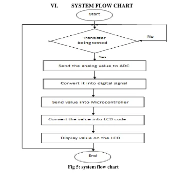
VI.
SYSTEM FLOW CHART
Fig 5: system flow chart
VIN+ 6 VIN-7 VREF/2 9 CLK IN 4 A GND 8 RD 2 WR 3 INTR 5 CS 1 D GND 10 DB7(MSB) 11 DB6 12 DB5 13 DB4 14 DB3 15 DB2 16 DB1 17 DB0(LSB) 18 CLK R 19 VCC 20 U2
ADC0804 18 XTAL2
XTAL1 19 ALE 30 EA 31 PSEN 29 RST 9 P0.0/AD0 39 P0.1/AD1 38 P0.2/AD2 37 P0.3/AD3 36 P0.4/AD4 35 P0.5/AD5 34 P0.6/AD6 33 P0.7/AD7 32 P1.0/T2 1 P1.1/T2EX 2 P1.2 3 P1.3 4 P1.4 5 P1.5 6 P1.6 7 P1.7 8 P3.0/RXD 10 P3.1/TXD 11 P3.2/INT0 12 P3.3/INT1 13 P3.4/T0 14 P3.7/RD 17 P3.6/WR 16 P3.5/T1 15 P2.7/A15 28 P2.0/A8 21 P2.1/A9 22 P2.2/A10 23 P2.3/A11 24 P2.4/A12 25 P2.5/A13 26 P2.6/A14 27 U3 AT89C52 R1 10k C1 150p D 7 1 4 D 6 1 3 D 5 1 2 D 4 1 1 D 3 1 0 D 2 9 D 1 8 D 0 7 E 6 R W 5 R S 4 V S S 1 V D D 2 V E E 3 LCD LM016L RV1 10k Q1 R8 1k R2 1k R9 1k R10 1k Q6 R3 2k D1 DIODE D2 DIODE NPN TESTED TRANSISTOR
VII.
DISCUSSION
LCD (Liquid Crystal Display) screen is an electronic display module. A 16x2 LCD display is very basic module and is very commonly used in various devices and circuits. These modules are preferred over seven segments and other multi segment LEDs. The reasons being: LCDs are economical; easily programmable; have no limitation of displaying special and even custom characters (unlike in seven segments), animations and so on.
A16x2 LCD means it can display 16 characters per line and there are 2 such lines. In this LCD each character is displayed in 5x7 pixel matrix. This LCD has two registers, namely, Command and Data.
The command register stores the command instructions given to the LCD. A command is an instruction given to LCD to do a predefined task like initializing it, clearing its screen, setting the cursor position, controlling display etc. The data register stores the data to be displayed on the LCD. The data is the ASCII value of the character to be displayed on the LCD.
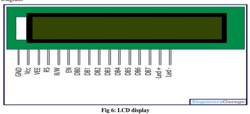
Pin Diagram:
Fig 6: LCD display
VIII.
CALCULATING THE LCD RESISTOR VALUE
An LCD must have a resistor connected in series to limit the current through the LCD, otherwise it will burn out almost instantly.
The resistor value, R is given by: Vs = supply voltage
VL = LCD current (usually 2V)
I = LCD current (e. g. 20mA), this must be less than the maximum permitted value.
If the calculated value is not available we choose the nearest standard resistor value which is greater, so that the current will be a little less than you chose. In fact you may wish to choose a greater resistor value to reduce the current (to increase battery life for example) but this will make the LCD less bright. If the supply voltage Vs=9V, and you have an LCD (VL = 2V), requiring a current I = 20mA = 0.020A
R = (9V – 2V) /0.02A = 35oΩ, so choose 390Ω (the nearest standard value which is greater).
Working out the LCD resistor formula using Ohm’s law Ohm’s law says that the resistance of the resistor,
R = V/I, where: V = voltage across the resistor (= Vs – VL in this case) I = the current through the resistor
So R= (Vs – VL) /I
Pin Description:
Pin
7
8-bit data pins
DB0
8 DB1
9 DB2
10 DB3
11 DB4
12 DB5
13 DB6
14 DB7
15 Backlight VCC (5V) Lcd+
16 Backlight Ground (0V) Lcd-
IX.
CONCLUSION
Recent developments in science and technology provide a wide range scope of applications of high performance in testing electronic devices with the use of a transistor tester. Certain problems were encountered during the design of this project, especially the problem of short circuit. Yet, this project is considered quite successful in the sense that it is functional in all operations and all the objectives of the project is achieved as earlier planned. There was no necessity to modify or amend the project plan or use different devices. All the tasks were carried out as planned and the steps used were purely based on the suitability with supervisor’s approval.
REFERENCES
[1]. J. Lim and A. Oppenheim (1988): Advanced Topics in Digital Processing. Prentice Hall limited, New Delhi 2nd edition. Pg 567.
[2]. Edward Roll Tuft (1990): Principles of Information display. Graphic Press Canada, 3rd edition. Pg 890 and 989.
[3]. B. BORAT (1997) : A course in digital processing Wiley 6th edition. Smith Publisher Washington. Pg 58-63
[4]. Lawrence A. Duarte (1998): The Microcontroller Beginner’s Handbook. 2nd Edition. United States of America: Prompt Publication. pg 3-5.
[5]. Joseph Greenfield (1999): Digital Electronic Design. Oxford University press 4th edition. Pg 89,567,905 and 1023.
[6]. Mcdraw Archer (2000): Advanced Digital Electronics, Oxford University press, 2nd edition. Pg 456 and 789.
[7]. Van Staveren and Arthur Roermond (2000): Structured Electronic Design, Springer Publishers New York. 5th edition. Pg 4, 6, 11-15.
[8]. Muhammad H. Rashid (2004): Power Electronics Circuits, Devices and Applications. 3rd edition. United States of America: Springer publishers.
Aru, Okereke Eze is a lecturer in the Department of Computer Engineering, Michael Okpara University of Agriculture, Umuahia, Abia State, Nigeria. His research Interests include Computational Intelligence, Computer Hardware design and maintenance, Security system design, , Expert systems and Artificial Intelligence, Design of Microcontroller and Microprocessor based system, digital systems design using microcontrollers and other computer related subjects.
Email: [email protected]
Prof. Ogbonnaya Okoro is a senior research fellow in the Department of Electrical/Electronic Engineering and the Dean of the College of Engineering, Michael Okpara University of Agriculture, Umuahia, Abia State, Nigeria. His research interests include Electrical Power and Machines, Control Systems, Architecture of Computerised Electrical Machines, etc.