Embedded Control Systems for Moving LCD
Display using 89C51 Microcontroller
Dr. Nirmesh B. Patel Head of Department
N. P. College of Computer Studies & Management, Kadi-383715, India
Abstract
In this project, we will have brief discussion on how to interface 16×2 LCD module to AT89C51, which is an 8051 family microcontroller. We use LCD display for the displaying messages in a more interactive way to operate the system or displaying error messages etc. Interfacing 16×2 LCD with 8051 microcontroller is very easy if you understanding the working of LCD Hence, in this project, I will not only give the information of LCD and also provide the code in using machine language which is working fine without any errors.
Keywords: Control Systems
________________________________________________________________________________________________________
I. INTRODUCTION
What is Embedded Control?
Microprocessor controlled system have become ubiquitous in our day-to-day lives. In addition to the microprocessor's familiar role as the central processing unit (CPU) in a computer, it is well suited to serve as a dedicated controller for various applications. A microprocessor used in a specific application is called a microcontroller. The embedded control field is simply defining the need for a microcontroller in a specific system and developing the hardware and software necessary for proper use and functioning of the microcontroller.
Why is Embedded Control Important to me?
Embedded devices are all around us, in many common items that we use. From the time you woke up this morning, you’ve probably interacted with at least five different systems which utilize a microprocessor and didn't even realize it. For example, most of you have a digital alarm clock which may have a small microprocessor in it. If you switched on your late-model stereo, then you’ve probably interacted with another microprocessor. If you cooked your breakfast or lunch in a microwave, then you’ve communicated your cooking instructions to its microprocessor. If you chose instead to eat in the school commons and paid by a credit account, then a microprocessor in the card reader of the cash register processed your transaction. If you drove to class and your car has fuel injection, then your car also utilizes a microprocessor. If you talked on your cell phone today, your voice went to a microprocessor which had it converted to a digital signal to be transmitted to a cell tower.
II.MICROCONTROLLER OVERVIEW
Fig. 1: Pin diagram of MC AT89C51
Pin Configurations
VCC Supply voltage.
GND Ground.
Port 0
Port 0 is an 8-bit open drain bidirectional I/O port. As an output port each pin can sink eight TTL inputs. When 1s are written to port 0 pins, the pins can be used as high-impedance inputs. Port 0 may also be configured to be the multiplexed low order address/data bus during accesses to external program and data memory. In this mode P0 has internal pull-ups. Port 0 also receives the code bytes during Flash programming, and outputs the code bytes during program verification. External pull-ups are required during program verification.
Port 1
Port 1 is an 8-bit bidirectional I/O port with internal pull-ups. The Port 1 output buffers can sink/source four TTL inputs. When 1s are written to Port 1 pins they are pulled high by the internal pull-ups and can be used as inputs. As inputs, Port 1 pins that are externally being pulled low will source current (IIL) because of the internal pull-ups. Port 1 also receives the low-order address bytes during Flash programming and program verification.
Port 2
Port 2 is an 8-bit bidirectional I/O port with internal pull-ups. The Port 2 output buffers can sink/source four TTL inputs. When 1s are written to Port 2 pins they are pulled high by the internal pull-ups and can be used as inputs. As inputs, Port 2 pins that are externally being pulled low will source current (IIL) because of the internal pull-ups. Port 2 emits the high-order address byte during fetches from external program memory and during accesses to external data memory that uses 16-bit addresses (MOVX @ DPTR). In this application it uses strong internal pull-ups when emitting 1s. During accesses to external data memory that uses 8-bit addresses (MOVX @ RI), Port 2 emits the contents of the P2 Special Function Register.
Port 3
Port 3 is an 8-bit bidirectional I/O port with internal pull-ups. The Port 3 output buffers can sink/source four TTL inputs. When 1s are written to Port 3 pins they are pulled high by the internal pull-ups and can be used as inputs. As inputs, Port 3 pins that are externally being pulled low will source current (IIL) because of the pull-ups. Port 3 also serves the functions of various special features of the AT89C51 as listed below:
Port Pin Alternate Functions
P3.3 INT1 (external interrupt 1) P3.4 T0 (timer 0 external input) P3.5 T1 (timer 1 external input)
P3.6 WR (external data memory write strobe) P3.7 RD (external data memory read strobe)
Port 3 also receives some control signals for Flash programming and programming verification.
RST
Reset input. A high on this pin for two machine cycles while the oscillator is running resets the device.
ALE/PROG
Address Latch Enable output pulse for latching the low byte of the address during accesses to external memory. This pin is also the program pulse input (PROG) during Flash programming. In normal Operation ALE is emitted at a constant rates of 1/6 the oscillator frequency, and may be used for external timing or clocking purposes. Note, however, that one ALE pulse is skipped during each access to external Data Memory. If desired, ALE operation can be disabled by setting bit 0 of SFR location 8EH. With the bit set, ALE is active only during a MOVX or MOVC instruction. Otherwise, the pin is weakly pulled high. Setting the ALE-disable bit has no effect if the microcontroller is in external execution mode.
PSEN
Program Store Enable is the read strobe to external program memory. When the AT89C51 is executing code from external program memory, PSEN is activated twice each machine cycle, except that two PSEN activations are skipped during each access to external data memory.
EA/VPP
External Access Enable. EA must be strapped to GND in order to enable the device to fetch code from external program memory locations starting at 0000H up to FFFFH. Note, however, that if lock bit 1 is programmed, EA will be internally latched on reset. EA should be strapped to VCC for internal program executions. This pin also receives the 12-volt programming enable voltage (VPP) during Flash programming, for parts that require 12-volt VPP.
XTAL
Input to the inverting oscillator amplifier and input to the internal clock operating circuit.
XTAL2
Output from the inverting oscillator amplifier. (C1, C2 = 30 pF ± 10 pF for Crystals
= 40 pF ± 10 pF for Ceramic Resonators)
Interfacing LCD with 8051
LCD is tongue of embedded system. With help of LCD, embedded system can communicate their status to external world. Two types of LCD modules are available; text and graphical. In this tutorial we will cover text based modules. LCD module JHD162A is used as example here, however same instructions would also apply for controller HD44780 which is one of most commonly used module. This tutorial is divided into following sections:
Interfacing hardware
Interfacing Hardware…
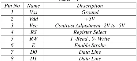
Let’s start with connecting the LCD hardware with microcontroller (P89v51). The following table lists all pins of LCD module (JHD162A) along with their description.
Table – 1
Pin No Name Description
1 Vss Ground
2 Vdd +5V
3 Vee Contrast Adjustment -2V to -5V
4 RS Register Select
5 RW 1 -Read , 0- Write
6 E Enable Strobe
7 D0 Data Line
9 D2 Data Line
10 D3 Data Line
11 D4 Data Line
12 D5 Data Line
13 D6 Data Line
14 D7 Data Line
15 LED+ Backlit LED +V Vdd (Optional signal) 16 LED- Backlit LED –V Vss (Optional signal)
Connecting Supplies
Vss (Pin 1) is connected to board ground. Vdd (Pin 2) is connected to + 5V supply.
Vee (Pin 3) is connected using a variable resistance for adjusting contrast. LED- (Pin 16) is connected to GND
LED+ (Pin 15) is connected to Vdd Connecting Control and Data Signals
Control signal RS, RW and E are connected to IO Port pins. For data lines we can have two configurations 8 bit mode and 4 bit mode. In 8 bit mode all lines D0-D7 are connected to IO port pins of microcontroller. In 4 bit mode only D4-D7 are connected to IO port pins. The example code available in source section (at bottom of this article) uses the 4 bit mode as default, however 8 bit mode is also supported.
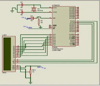
Hardware interfacing of 89C51 with LCD
Fig. 1: Hardware interfacing of 89C51 with LCD
Assembly Coding for Moving message display
Coding for 4 –bit mode ORG 0000h
MOV 36H, #'H'
CLR P1.3 ;clear RS for Sending command ;function set
CLR P1.7; high nibble send CLR P1.6 SETB P1.5 CLR P1.4 SETB P1.2 CLR P1.2 CALL delay SETB P1.2 CLR P1.2
CLR P1.7; low nibble send SETB P1.2
CLR
[Moving LCD Display] Page 15
CALL delay; wait for buffer(BF) to clear ; entry mode set
CLR P1.7 CLR P1.6 CLR P1.5 CLR P1.4 SETB P1.2 CLR P1.2 SETB P1.6 SETB P1.5 SETB P1.2 CLR P1.2 CALL delay
; display on/off control CLR P1.7 CLR P1.6 CLR P1.5 CLR P1.4 SETB P1.2 CLR P1.2 SETB P1.7 SETB P1.6 SETB P1.5 SETB P1.4 SETB P1.2 CLR P1.2 CALL delay ; send data back:
SETB P1.3 ; clear RS for sending the data MOV R1, #30H
loop:
MOV A, @R1 JZ finish CALL send INC R1 JMP loop send:
MOV C, ACC.7 ;send High nibble of data MOV P1.7, C
MOV C, ACC.4 MOV P1.4, C SETB P1.2 CLR P1.2
MOV C, ACC.3 ;send low nibble of data MOV P1.7, C
MOV C, ACC.2 MOV P1.6, C MOV C, ACC.1 MOV P1.5, C MOV C, ACC.0 MOV P1.4, C SETB P1.2 CLR P1.2 delay:
MOV R0, #30H DJNZ R0, $ RET finish: NOP
MOV R2,#08h CLR P1.3 moving:
MOV A,#1CH ;send code for shifting display right MOV C, ACC.7
MOV P1.7, C MOV C, ACC.6 MOV P1.6, C MOV C, ACC.5 MOV P1.5, C MOV C, ACC.4 MOV P1.4, C SETB P1.2 CLR P1.2 LCALL DELAY MOV C, ACC.3 MOV P1.7, C MOV C, ACC.2 MOV P1.6, C MOV C, ACC.1 MOV P1.5, C MOV C, ACC.0 MOV P1.4, C SETB P1.2 CLR P1.2
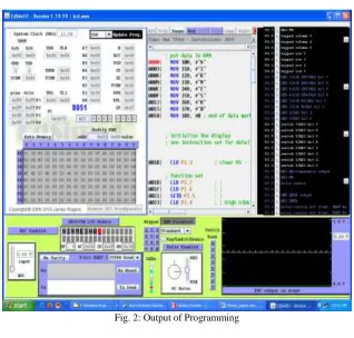
III. OUTPUT OF PROGRAMMING
Fig. 2: Output of Programming
IV. CONCLUSION
Our vision of model-based development rests on two pillars: Explicit product models, which for the developer appear as domain-specific languages, and explicit process models, which define the developer’s activities that transform early, abstract, partial products to the final, concrete and complete products that are ready to be delivered and deployed.
The benefits of model-based development come from the interaction of process and product models and their realization in a CASE tool: Firstly, complex design steps such as refractoriness or the introduction of complex communication patterns [11] between components can be naturally defined and performed in a tool. Secondly, the application of such design steps naturally leads to a development history that can be recorded in the tool and used for a kind of high-level configuration and version management. Finally, the requirements and design rationales that influence design steps can be traced and documented throughout the complete development process.
However, model-based development is not without risk. It is not obviously clear whether a seamless development process from early design to final target code is feasible: Some design steps might demand knowledge of environment properties which are difficult to formalize. Design steps in the later phases will require precise knowledge of the target platform, for instance to access device drivers or in order to estimate the worst case execution times which are needed as input for scheduling algorithms.
REFERENCES
[1] G. Kiczales, “Aspect-Oriented Programming: The Fun Has Just Begun,” Software Design and Productivity Coordinating Group – Workshop on New Visions for Software Design and Productivity: Research and Applications, Nashville, Tennessee, December 2001.
[2] J. Gray, T. Bapty, S. Neema, A. Gokhale, “Aspect-Oriented Domain- Specific Modeling,” [Online]. Available: http://www.isis.vanderbilt.edu/ projects/PCES/AODM.pdf.
[3] http://eclipse.org/aspectj/. [4] http://www.aspectc.org/.
[5] “Bringing Aspects into Deeply Embedded Devices,” AOSD 2003 Conference, fileadmin/publications/aosd-2003-demo.pdf.
[6] D. Mahrenholz, O. Spinczyk, W. Schroder-Preikschat, “Program instrumentation for debugging and monitoring with AspectC++,” Proceedings Fifth IEEE International Symposium on Object-Oriented Real-Time Distributed Computing, ISIRC 2002, pp. 249-56.
[7] A. Gal, W. Schröder-Preikschat, O. Spinczyk, “AspectC++: Language Proposal and Prototype Implementation,” the OOPSLA 2001 Workshop on Advanced Separation of Concerns in Object-Oriented Systems, Tampa, Florida, October 14th, 2001.
[8] J. Sztipanovits, G. Karsai, “Model-integrated computing,” Computer, vol. 4, no.30, April 1997, pp. 110-111. [9] K. Beck. Extreme Programming Explained: Embrace Change. Addison Wesley, 1999.
[10] K. Bender, M. Broy, I. P´eter, A. Pretschner, and T. Stauner. Model based development of hybrid systems: specification, simulation, test case generation. In Modelling, Analysis and Design of Hybrid Systems, LNCIS. Springer, 2002. To appear.
[11] Jean-Claude Derniame, Badara Ali Kaba, and David Wastell, editors. Software Process: Principles, Methodology and Technology. Springer, 1999. LNCS 1500.
[13] D. Harel. Biting the silver bullet: Toward a brighter future for system development. IEEE Computer, 25(1), January 1992.
[14] Thomas A. Henzinger, Benjamin Horowitz, and Christoph Meyer Kirsch. Giotto: A time-triggered language for embedded programming. In Proceedings of EMSOFT 2001, LNCS 2211, 2001.
[15] Franz Huber and Bernhard Sch¨atz. Integrated Development of Embedded Systems with AutoFocus. Technical Report TUMI-0701, Fakult¨at f¨ur Informatik, TUM¨unchen, 2001.