IJSRST173768 | Received : 15 Sep 2017 | Accepted : 30 Sep 2017 | September-October-2017 [(3) 7: 408-413]
© 2017 IJSRST | Volume 3 | Issue 7 | Print ISSN: 2395-6011 | Online ISSN: 2395-602X Themed Section: Science and Technology
408
Effect of Nonparabolicity of Conduction Band on Temperature Dependent
Electron Mobility in III-V Compounds
A. K. Ghorai
Physics Department, Kalimpong College, Kalimpong, West Bengal, India
ABSTRACT
The effect of nonparabolicity of the conduction band on the zero-field mobility of free electrons in bulk semiconductor is calculated at low lattice temperatures using relaxation time approximation and taking into account some elastic scattering mechanisms. The mobility expressions are considered for the interaction of electrons with the ionized impurity atoms, the deformation potential acoustic phonons and the piezoelectric acoustic phonons both for parabolic and nonparabolic conduction band. The numerical computations are carried out in InSb, a III-V compound having high value of nonparabolicity factor and in GaAs, a III-V compound semiconductor with low value of nonparabolicity factor. Numerical calculation is done for ionized impurity concentrations of
and in both the samples and it is observed that the nonparabolicity of the conduction band
affects the electron mobility noticeably.
Keywords: Semiconductor, Electron, Scattering Rates, Phonon, Mobility.
I.
INTRODUCTION
The results of theoretical studies on the mobility of free electrons in semiconducting materials are important for their application in solid state electronic devices. Different theoretical models were developed to study the mobility characteristics and the success of these models needs the proper knowledge of the scattering mechanisms of the free electrons and the energy band structure of the material. The free electrons are scattered dominantly by optical and intervalley phonons at lattice temperatures above 100K and by impurities at very lower temperatures. Between these two extreme situations the free carriers in compound semiconductors interact rather strongly with deformation potential acoustic phonons and also with piezoelectric acoustic phonons if the bonds in the materials are partly ionic so that the unit cell does not contain a centre of symmetry [1-6]. The impurity scattering can be suppressed by dielectric engineering but the scattering by acoustic phonons is intrinsic to the semiconductor and cannot be eliminated.
The advanced Si technology has prompted most of the studies in semiconductor physics. With these studies a considerable number of works have also been initiated on III-V and II-VI compound semiconductors. An
Most of the studies on the transport characteristics of the free electrons in semiconductors are based on the assumption of a model semiconductor having parabolic dispersion law. This is the simplest band model for a semiconductor and it can be adopted only for rough estimate of the electrical transport properties under the condition that the free carriers may be assumed to be confined to a short segment of the energy dispersion curve near the minimum of the conduction band [13]. But no semiconductor is really known to possess a parabolic band structure. For a direct band gap semiconductor the minimum of the conduction band is situated in the centre of the Brillouin zone. Near the minimum, the energy is isotropic and the band may be assumed to be parabolic [13]. For values of wave vector far from the conduction band minima, the energy deviates from the simple quadratic expressions and nonparabolicity occurs. The present author have reported few studies on electron transport in elemental as well as compound semiconductors giving due account to the effect of nonparabolicity of the conduction band under different prevalent conditions of scattering mechanisms [5,6,9,10]. In those studies it has been observed that the nonparabolicity factor influences the transport parameters in a very complex manner. Thus it would be interesting to determine the lattice temperature dependent mobility expressions of the electrons in bulk semiconductor introducing the nonparabolicity factor in the calculation. In this article the zero-field mobility of non-degenerate electron ensemble is estimated both for parabolic and nonparabolic band structure considering ionized impurity scattering, deformation potential acoustic phonon and piezoelectric acoustic phonon scattering. Thus we may observe the effect of nonparabolicity on the temperature controlled electron mobility characteristics in semiconductors. The relaxation time approximation approach is used to investigate the mobility characteristics of free electrons taking into account elastic scattering mechanism types. The results are used to obtain the electron mobility in InSb and GaAs which have one of the highest and lowest values, respectively, of the nonparabolicity factor.
II.
Theoretical Model
The finite nonparabolicity factor ( ) of the conduction band is taken into account through
electron energy ( ) and wave vector ( ) relationship [8] of the form
( ) ( ) ( ) Here is the Dirac constant and is the effective mass of the electron at the bottom of the -point. For -point minimum
( )
where being the direct energy gap at -point, the rest mass of the free electron.
The zero-field electron mobility can be determined by solving Boltzmann equation in the relaxation time approximation as
〈 ( )〉 ( )
where 〈 ( )〉 is the average relaxation time over the electron energies, is the electronic charge and is the mobility effective mass of the electron.
The effective mobility ( ) can be calculated taking the individual contribution of the mobility ( ) by
ionized impurity scattering, the mobility ( ) by
deformation potential scattering and the mobility ( ) by piezoelectric scattering with the help of
the well-known Matthessen Rule as
( )
2.1 Ionized Impurity Scattering
then the impurity concentration can be used in place of For the sample of our interest the doping concentration is low and hence the BH-approach will be more appropriate. Using the expression of relaxation time for impurity scattering calculated by BH-approach [4] the temperature dependent mobility of the free electrons for spherical parabolic band can be given as
( )
√ (
) ( )
where
√ ⁄
for non-degenerate ensemble.
Here is the static dielectric constant of the material, is the number of charge units of the impurity and
is the Boltzmann constant.
If we use the expression for the momentum relaxation time of an electron obtained in the light of BH-approach [4] for spherical nonparabolic band then the electron mobility can be given as
( )
( ) ( )
where √ ⁄
( )
{ ( ) ( ) ( ) ( )}
( ) { ( ) }
( ) { ( )
}
Here ( ) is the incomplete Gamma function.
2.2 Acoustic Phonon Scattering
Electrons are not scattered by ideal periodic potentials associated with the periodic array of ions constituting the crystal. However, due the lack of periodicity due to various reasons, electrons are scattered by lattice vibrations propagating in the crystal. The deviation of the crystal potential from pure periodicity may be expressed by the amplitude of the lattice vibrations due to a small displacement of an ion in the crystal causes a small change in the crystal potential. This deviation from the periodicity is generally expressed in a rather phenomenological way as the deformation potential method because of the difficulty of knowing the crystal potential itself. The influence of lattice vibrations on
electron motions can be expressed by a quantum process since the wave nature of the lattice vibrations can be quantized as phonons. This process is termed the electron-phonon scattering [14].
2.2.1 Deformation Potential Scattering
The acoustic mode lattice vibration induces changes in lattice spacing, which change the band gap from point to point. Since the crystal is "deformed" at these points, the potential associated is called the deformation potential. Using the corresponding relaxation time for parabolic band structure the mobility associated with the deformation potential scattering can be written as [1, 2]
( )
( )
where
√
being the deformation potential constant, the crystal mass density, being the average sound velocity through the crystal.
When the expression of relaxation time for nonparabolic band [3, 5] is considered the zero-field mobility of free electrons for the deformation potential scattering can be obtained as
( ) ( ) ( )
where
√ ⁄ ⁄
( ) ( )
( ) ( ) (
)
( ) (
)
( ) ( )
2.1.2 Piezoelectric Scattering
semiconductor when there is no inversion symmetry in the crystal. The electron mobility due to this effect can be written for parabolic band as [1, 2]
( ) ( )
where
√
being the piezoelectric coupling constant.
When the expression of relaxation time [3, 5] for nonparabolic band is considered then the mobility of electrons associated with the piezoelectric scattering can be written as
( ) ( ) ( )
where
√
( ) ( )
( ) ( ) (
)
( )
(
)
( ) (
)
III.
Result and Discussion
From the Eqns.(4) to (9), it is noticeable that the mobility values depend on lattice temperature in a very complex manner when nonparabolicity of the conduction band is taken into account in comparison to what follows for the parabolic band structure. For the application of the above formulation we consider the most important III-V semiconductors InSb and GaAs which have one of the highest and lowest values, respectively, of the nonparabolicity factor. To observe the effect of nonparabolicity on the electron mobility in InSb and GaAs in a temperature range from 1K up to 100K and for different ionized impurity concentrations, we use the material parameters of these materials listed in Table-1.
Table-1
Material parameters of InSb and GaAs [11, 12]
Physical constants InSb GaAs
Deformation potential,
(eV) 30.0 12.0
Effective mass
ratio( ⁄ ) 0.0145 0.067
Acoustic velocity,
( ) 3.7 5.2 Density, ( ) 5.78 5.31
Nonparabolicity factor,
( ) 5.72 0.64
Piezoelectric coupling
constant, 0.027 0.052
Static dielectric constant,
17.9 13.5
Fig.1 and Fig.2 the lattice temperature controlled electron mobility is plotted for both parabolic and nonparabolic band. From the figures it is seen that at very low lattice temperatures the ionized impurity scattering dominantly controls the electron transport. The mobility assumes higher value for higher concentration of the ionized impurity and the mobility becomes independent of ionized impurity concentration at lattice temperatures higher than 20K or so both for parabolic as well as nonparabolic band.
From the figures it is observed that the temperature dependent electron mobility decreases rapidly with the rise of lattice temperature both for parabolic and nonparabolic band. In both cases the qualitative dependence is almost the same but due to nonparabolicity of the conduction band the electron mobility is less in comparison to what follows for the parabolic band. Again with the rise of lattice temperature the mobility values decreases more and more due to the effect of nonparabolic band. It is because the carriers become more energetic due to high lattice temperature and the nonparabolicity comes into effect.
To estimate the effect of nonparabolic band on the mobility of the electrons we may calculate the percentage deviation as
( )
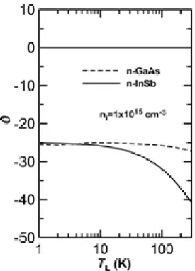
Fig.3 shows how the percentage deviation of the zero-field mobility due to nonparabolicity of the conduction band in InSb and GaAs depends upon the lattice temperature. Since is always negative, the finite nonparabolicity affects as lower value of temperature dependent electron mobility in comparison to that corresponding to a parabolic band. The magnitude of assumes a finite value at low lattice temperature. Initially it increases slowly with the rise of lattice temperatures and later on it increases at a much faster rate when the lattice temperature becomes relatively higher.
Figure 3. Dependence of percentage deviation of mobility upon lattice temperature due to
nonparabolicity
IV.
Conclusion
In the present investigation we have calculated the electron mobility considering the effect of nonparabolic conduction band. In the study we observe that the finite nonparabolicity affects the mobility values particularly when the free carriers are energetic. Thus we may conclude that in the study of electron transport in semiconductors under high-field condition or at higher temperatures, the effect of nonparabolicity has to be given due consideration.
V.
REFERENCES
[1] E. M. Conwell, High Field Transport in Semiconductors, Academic Press, New York, 1967.
[2] L. Reggiani, Hot-Electron Transport in Semiconductors, Springer-Verlag, Berlin, 1985. [3] B. R. Nag, Electron Transport in Compound
Semi-conductors, Springer-Verlag, Berlin, 1980. [4] C. Jacoboni and L. Reggiani, “The Monte Carlo
method for the solution of charge transport in semiconductors with applications to covalent materials”, Rev. Mod. Phys., vol. 55, no. 3, pp. 645-705, 1983.
[5] A. K. Ghorai and D. P. Bhattacharya, “Effect of Non-Parabolic Band on the Scattering Rates of Free Electrons in High Purity Semiconductors at Low Lattice Temperatures”, phys. stat. sol.(b), vol. 163, pp. 247-258, 1991.
mobility characteristics of high-purity semiconductors at low lattice temperatures”, Phys. Rev. B, vol. 47, no. 20, pp.13858-13860, 1993. [7] W. Fawcett, A. D. Boardman and S. S. Swain,
“Monte Carlo determination of electron transport properties in gallium arsenide”, J. Phys. Chem. Solids, vol. 31, no. 9, pp. 1963-1990, 1970. [8] E. M. Conwell and M. O. Vassel, “High-Field
Transport in n-type GaAs”, Phys. Rev. vol. 166, pp. 797, 1968.
[9] A. K. Ghorai and D. P. Bhattacharya, “Non-equilibrium carrier transport in III-V compounds at low lattice temperatures”, Physica B, vol. 212, pp. 158-166, 1995.
[10] A. K. Ghorai and D. P. Bhattacharya, “Electron transport in GaAs at low lattice temperatures”, phys. stat. sol.(b), vol.197, pp. 125-136, 1996. [11] A. K. Ghorai and D. P. Bhattacharya,
“Lattice-controlled electron transport characteristics in quantized surface layers at low temperature”, Surf. Sci., vol. 380, no. 2-3, pp. 293-301, 1997.
[12] A. K. Ghorai, “Phonon Controlled Temperature Dependence of Electron Mobility in 2DEG of GaAs Surface Layer”, IJSRST, vol.3, no. 6, pp. 281-287, 2017.
[13] C. Jacoboni and L. Reggiani, “Bulk hot-electron properties of cubic semiconductors”, Adv. In Phys.. vol 28, no.4, pp. 493-553, 1979.
![Table-1 Material parameters of InSb and GaAs [11, 12]](https://thumb-us.123doks.com/thumbv2/123dok_us/9112827.1445715/4.595.194.535.46.700/table-material-parameters-insb-gaas.webp)