Dynamics of IGBT based PWM
Converter
A Case Study
Navpreet Singh Tung
M-Tech Scholar, Electrical Engg. , Lovely Professional University ,India [email protected]
Amit Bhardwaj
M-Tech Scholar, Electrical Engg. , Lovely Professional University ,India [email protected]
Tarun Mittal
M-Tech Scholar, Electrical Engg. , Lovely Professional University ,India [email protected]
Vijay Shukla
Electrical Engg. , Lovely Professional University
Abstract— Optimizing the efficiency and dynamics of power converters is a critical tradeoff in power electronics. The increase of switching frequency can improve the dynamics of power converters, but the efficiency may be degraded as well as the switching losses. As power semiconductor devices like diodes, MOSFETS, IGBTs, Thyristors, BJTs have their own characterstics and dynamic responses. It is desired to analyze and observe the dynamics of different semiconductor devices before they actually employed in the model. Inclusion of different PWM techniques help in the removal of power line interferences like harmonic losses, unwanted ripples, chopped frequencies, spikes. In this paper, we have studied and analyzed the dynamics of IGBT based PWM converter with subjected to different conditions like transient state, steady state feeding the RLC load. Snubber circuits are used to reduce the switching losses. The IGBT based PWM converter reflects the better dynamics with improved efficiency and reduced harmonics as compared to some other power semiconductor devices when FFT is performed and subjected to standard parameterized RLC load under steady state and transient analysis.
Index Terms – Modulation Index(MI),Pulse Width Modulation(PWM),FFT(Fast Fourier Transform)
1. Introduction
THE DEMAND of high performance power converter is increased exponentially with the increasing spectrum of power converter’s application fields [1]. In order to optimize the transient and steady state performance of power converters and to enhance power density, high switching frequency is an effective method. However, switching frequency rise causes higher switching losses and greater EMI losses [2]. This, in turn, lim
capacitor ripple voltage is determined by the low frequency. Hence, this topology is not suitable for improvement of dc output transient and steady state performances. Moreover, the main Boost circuit and the added cell are coupled, and the added Boost cell has an effect on the inductor current input [15]. Splitting the filter inductor of buck converter into two parts with added auxiliary active switch and diode has been proposed to improve the output voltage response at load current down transient situation, but not at load current step-up transient situation [16]. Additional transformer and switches are needed to realize the improvement at step-step-up transient [17]. To make the circuits in [16] and [17] function as designed, it is required to detect the load transient event, then to trigger or shut down the auxiliary switch. This increases the complexity of the control circuit. Moreover, oscillations at the output voltage occur due to the frequent on and off operations at each transient event. On the other hand, high-frequency switching converter or linear power supply in parallel with low-frequency converter proposed in [18] and [19] enhances the output voltage response. Paralleling high-frequency converter approach also requires the load transient information, while linear power supply method suffers from low efficiency. Moreover, the parallel structure brings about the circulating current problem. Additional current sharing control is needed to overcome this problem.
2. Model Layout
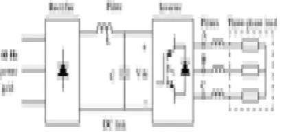
A 60 Hz, voltage source feeds a 50 Hz, 50 kW load through a double conversion converter. The 600V, 60 Hz voltage obtained at secondary of the Y connected transformer is first rectified by a six pulse diode bridge. The filtered DC voltage is applied to an IGBT two-level inverter generating 50 Hz. The IGBT inverter uses PWM at a 2 kHz carrier frequency. The circuit is discretized at a sample time of 2 us The load voltage is regulated at 1 pu (380 V rms) by a PI voltage regulator using abc_to_dq and dq_to_abc transfomations. The first output of the voltage regulator is a vector containing the three modulating signals used by the PMW Generator to generate the 6 IGBT pulses. The second output returns the modulation index. The Discrete 3-Phase PWM Pulse Generator is used.
Fig 3. Schematic of PWM Converter
3. Performance Analysis
3.1 Steady State Analysis
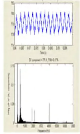
After a transient period of approx. 50 ms, the system reaches a steady state as observed in Fig.4. Observe voltage waveforms at DC bus, inverter output and load. Harmonics generated by the inverter around multiples of 2 kHz are filtered by the LC filter. As expected the peak value of the load voltage is 537 V (380 Vrms). In steady state, the mean value of the modulation index is m = 0.80 and the mean value of the DC voltage is 778 V. The fundamental component of 50 Hz voltage in the chopped inverter voltage is therefore:
Vab = 778 V * 0.612 * 0.80 = 381 V rms
3.2 FFT Analysis
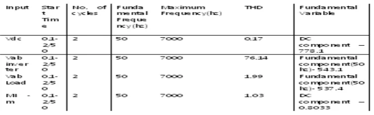
'FFT Analysis' displays the 0 - 7000 Hz frequency spectrum of signals as shown in Fig.6(a,b,c,d). The FFT is performed on a 2-cycle window starting at t=0.1-2/50 (last 2 cycles of recording). For load voltage- 'Vab Load' observe the frequency spectrum of last 2 cycles. Notice harmonics around multiples of the 2 kHz carrier frequency. Maximum harmonic is 1.4 % of fundamental and THD is 2%.
Table 1. FFT Analysis
Fig 4. Variation of Vdc, Vab_inverter, Vab_load, m Fig 5 . Variation of Diode currents and Switches (IGBT)
Fig 6.a – Vdc FFT Analysis Fig 6.b Vab inverter FFT Analysis
Fig 6.c Vab load FFT Analysis Fig 6.d – MI(m) FFT Analysis
Figure 7. Diode bridge Figure. 8– Initial values of parameters
5. Circuit Analysis
5.1 3 phase IGBT PWM Inverter(Fig.2)
It implements a universal three-phase power converter that consists of up to six power switches connected in a bridge configuration with forced-commutated device- IGBT. Series RC snubber ckt is connected parallel to lower down the switching losses on IGBT.
The bridge operates satisfactorily with purely resistive snubbers as long as firing pulses are sent to switching devices. If firing pulses to forced-commutated devices are blocked, only anti-parallel diodes operate, and the bridge operates as a diode rectifier. In this condition appropriate values of Rs and Cs must also be used. When the system is discretized, use the following formulas to compute approximate values of Rs and Cs:
a)Rs >2 Ts/Cs
(u-micro, o-ohm, m-milli, s-seconds,inf-infinite)
Parameter Description Value
Lon Internal Inductance 0 Ron Internal Resistance 1mo Rs Snubber Resistance 5000o Cs Snubber Capacitance inf Vdf Diode forward voltage 0 Vf IGBT forward voltage 0 Tf Fall time(IGBT) 1us Tt Tail time(IGBT) 2us
5.2 3 phase voltage Source in series with RL branch
Table 3.Parameters of the block
Parameter Value V(phase to phase rms)(V) 25000 Phase angle of phase A(degree) 0 3 phase short circuit level at base voltage(VA) 106 Base Voltage rms(V) 25000 Frequency (hz) 60
Ratio X/R 5
The internal inductance L (in H) is computed from the inductive three-phase short-circuit power Psc (in VA), base voltage Vbase (in Vrms phase-to-phase), and source frequency f (in Hz) as follows:
L=(Vbase)2*1/(2*3.14*F*Psc) Where Psc – short circuit level(VA)
5.3 3 phase transformer
The leakage inductance and resistance of each winding are given in p.u. based on the transformer nominal power Pn and on the nominal voltage of the winding (V1(primary)-V2(secondary)).
Table 4.Parameters of the block
Parameter Value(pu) Pn(VA) - nominal 50000
Fn(hz)- nominal 60
V1ph-ph(rms) 25000
L1 0.02 R1 0.004 V2ph-ph(rms) 600
L2 0.02 R2 0.004 Rm(magnetization) 200
Lm(magnetization) 200
1- Primary side 2- Secondary side
5.4 3 phase diode rectifier bridge(Fig7)
It consists of three-phase diode power converter that consists of up to six power switches connected in a bridge configuration.
Table 5.Parameters of the block
Parameters Value Rs(ohm) 100
Cs(Farad) 0.1x10⁻⁶
Ron(ohms) 1x10⁻³
Lon(H) 0 Vf(V) 0.8
5.5 LC filter
As the output of inverter contains harmonic components of multiples of fundamental frequency component, an LC filter is used to remove all these harmonics as shown in fig.3.
L=3 mh
Reactive power( Capacitive) – 3 KVAR
5.6 3 phase load
QC(reactive power capacitive in – vars)
0
5.7 Voltage Regulator
The load voltage is regulated at 1 pu (380 V rms) by a PI voltage regulator using abc_to_dq and dq_to_abc transfomations The first output of the voltage regulator is a vector containing the three modulating signals used by the PMW Generator to generate the 6 IGBT pulses. The second output returns the modulation index. The Discrete 3-Phase PWM Pulse Generator is used. One input is used as reference in per unit whose value is set as constant 1.Other input is 3 phase voltage in per unit refer as Vabc (pu).The conversion is done as below –
Vabc(pu)=Vabc(volts)/((VbaseLL/1.71)*1.41 ) Where VbaseLL – Line to Line voltage in RMS.
Here, PI is used to remove steady state error in the model. Values are chosen carefully for the optimal operation of the circuit.
Proportional Gain Kp=0.4 Integral Gain Ki=500
5.8 Discrete PWM Generator
The three modulating signals used by the PMW Generator to generate the 6 IGBT pulses. The output pulses are a vector (with values=0 or 1). For a 3-arm bridge: Pulses 1,3 and 5 are respectively for the upper switches of the first, second and third arm. Pulses 2,4 and 6 are for the lower switches. External signals are used for pulse generation. The width of the input vector must be 3 for 3-phase bridges. It compares the modulating signal with carrier signal and generate pulses accordingly.
Fc(Carrier frequency in hz)=2000 Fm(Modulating frequency in hz)=50
6. Conclusion
In this paper, we have studied the dynamics of IGBT based PWM converter feeding the RLC Load. FFT is performed to analyze the steady state and transient analysis which results in significant reduction in the harmonic losses. Future work will incorporate to study the dynamics of other PWM techniques to enhance the performance using different power semiconductor devices for high current or high dynamics specifications.
References
[1] X. Zhou, P.-L. Wong, P. Xu, F. C. Lee, and A. Q. Huang, “Investigation of candidate VRM topologies for future microprocessors,” IEEE Trans. Power Electron., vol. 15, no. 6, pp. 1172–1182, Nov. 2000.
[2] U. Borup, F. Blaabjerg, and P. Enjeti, “Sharing of nonlinear load in parallel-connected three-phase converters,” IEEE Trans. Ind. Appl., vol. 37, no. 6, pp. 1817–1823, Nov./Dec. 2001.
[3] H. Mao, F. C. Lee, D. Boroyevich, and S. Hiti, “Review of high performance three-phase power-factor correction circuit,” IEEE Trans. Ind. Appl., vol. 44, no. 4, pp. 437–446, Aug. 1997.
[4] H. Pollock and J. O. Flower, “New method of power control for series–parallel load-resonant converters maintaining zero-current switching and unity power factor operation,” IEEE Trans. Power Electron., vol. 12, no. 1, pp. 103–115, Jan. 1997.
[6] C. M. Wang, “New family of zero-current-switching PWM converters using a new zero-current-switching PWM auxiliary circuit,” IEEE Trans. Ind. Electron., vol. 53, no. 3, pp. 768–777, Jun. 2006.
[7] S. K. Mazumder, A. H. Nayfeh, and D. Boroyevich, “A novel approach to the control of parallel three-phase boost converters that combines space vector modulation with variable-structure control,” in Proc. IEEE APEC,2002, pp. 1031–1037.
[8] Z. Ye, D. Boroyevich, J. Y. Choi, and F. C. Lee, “Control of circulating current in two parallel three-phase boost rectifiers,” IEEE Trans. Power Electron., vol. 17, no. 5, pp. 609–615, Sep. 2002.
[9] L. Asiminoaei, E. Aeloiza, P. Enjeti, and F. Blaabjerg, “Shunt activepower- filter topology based on parallel interleaved inverters,” IEEE Trans. Ind. Electron., vol. 55, no. 3, pp. 1175–1189, Mar. 2008.
[10] S. K. Mazumder, M. Tahir, and K. Acharya, “Master–slave currentsharing control of a parallel dc–dc converter system over an RF communication interface,” IEEE Trans. Ind. Electron., vol. 55, no. 1, pp. 59–66, Jan. 2008.
[11] C.-T. Pan and Y.-H. Liao, “Modeling and coordinate control of circulating currents in parallel three-phase boost rectifiers,” IEEE Trans. Ind. Electron., vol. 54, no. 2, pp. 825–838, Apr. 2007.
[12] Z. Ye, P. K. Jain, and P. C. Sen, “Circulating current minimization in high-frequency AC power distribution architecture with multiple inverter modules operated in parallel,” IEEE Trans. Ind. Electron., vol. 54, no. 5, pp. 2673–2687, Oct. 2007.
[13] G. C. Hua, C.-S. Leu, Y. Jiang, and F. C. Lee, “Novel zero-voltagetransition PWM converters,” IEEE Trans. Power Electron., vol. 9, no. 2,pp. 213–219, Mar. 1994.
[14] T. Yoshida, O. Shiizuka, O. Miyashita, and K. Ohniwa, “An improvement technique for the efficiency of high-frequency switch-mode rectifiers,” IEEE Trans. Power Electron., vol. 15, no. 6, pp. 1118–1123, Nov. 2000.
[15] H. Y. Kanaan, A. Marquis, and K. Al-Haddad, “Small-signal modeling and linear control of a dual boost power factor correction circuit,” in Proc. IEEE PESC, 2004, pp. 3127–3133.
[16] F. Zhang, J. Zhang, D. Xu, and Z. Qian, “A novel high performance voltage regulator module,” in Proc. IEEE APEC, 2001, pp. 258– 261.
[17] N. K. Poon, C. P. Liu, and M. H. Poon, “A low cost dc–dc stepping inductance voltage regulator with fast transient loading response,” in Proc. IEEE APEC, 2001, pp. 268–272.
[18] Mohan, N., T.M. Undeland, and W.P. Robbins, Power Electronics: Converters, Applications, and Design, John Wiley & Sons, Inc., New York, 1995.
[19] http://www.mathworks.com/