Application Note
Rev. 0, 01/2007
Contents
1
Introduction
Some refrigerators still have a basic electromechanical
circuit that controls the temperature. This application
shows how to implement a low-cost, basic temperature
control for refrigerators using the MC9RS08KA2. This
method can be implemented to control the temperature of
any device using a thermoresistor, a potentiometer,
resistors and a capacitor.
2
Requirements
•
MC9RS08KA2 microcontroller (MCU)
•
One potentiometer
•
One thermoresistor
•
One ceramic capacitor
•
Two ¼ watt resistors
•
CodeWarrior
™5.1 development tool
1 Introduction . . . 1
2 Requirements . . . 1
3 Implementation . . . 2
3.1 Control Value. . . 2
3.2 Temperature Sensor . . . 5
3.3 Temperature Control Application. . . 9
3.4 Schematic . . . 12
4 Conclusion. . . 12
Appendix A . . . NCP18WB333J03RB Thermistor Range Table. . . 13
Appendix B Code Implementation. . . 14
Basic Refrigerator Control Using
the MC9RS08KA2
by: Jose Ruiz RTAC Americas
3
Implementation
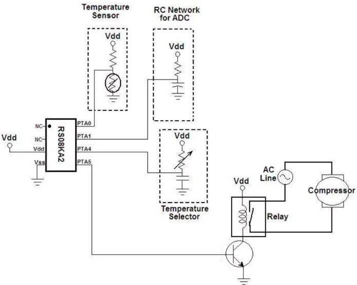
The temperature control is implemented with a single potentiometer and a capacitor connected to one
MC9RS08KA2 MCU I/O pin. The temperature sensor is a basic voltage divider formed by a resistor and
a thermistor. The output is an I/O pin connected to a relay that switches the supply of the refrigerator.
The flow of the program consists of reading the control wheel value followed by reading the sensor voltage
and, finally, switching the output ON or OFF according to the control and sensor values.
3.1
Control Value
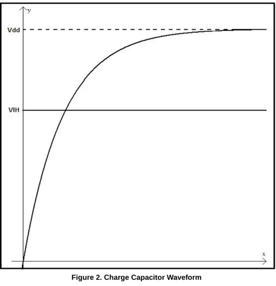
The refrigerator temperature control is a basic RC network connected to an I/O pin. By measuring the
charging time of the RC network, we can determine the potentiometer resistance, and therefore, the value
you entered. The charge curve of the RC network is used to determine the time the curve takes to go from
0 V to the input-high voltage (V
IH). This method is used because the MC9RS08KA2 MCU does not have
an integrated analog-to-digital converter (ADC).
Figure 1. Temperature Control Implementation
The first step is configuring the control pin as output. Set the pin value to 0 to discharge the capacitor. After
the capacitor is fully discharged, change the control pin direction to an input. The capacitor starts charging
to V
DD.
When the voltage of the capacitor gets to V
IH, the pin state changes from 0 to 1.
A variable resistor (potentiometer) is used to modify the time the capacitor takes to reach V
IH. Adjusting
Figure 2. Charge Capacitor Waveform
The capacitor voltage is given by the following equation:
Solving for time
•
Vc — Voltage of the capacitor
•
V
DD— Supply voltage of RC network
•
t — Time (seconds)
•
r — Resistance
•
c – Capacitor
A 10 k
Ω
potentiometer and 33 nF capacitor were used in this application note.
⎟⎟
⎠
⎞
⎜⎜
⎝
⎛
−
=
−rc te
Vdd
Vc
1
⎟
⎠
⎞
⎜
⎝
⎛ −
−
=
Vdd
Vc
rc
t
ln
1
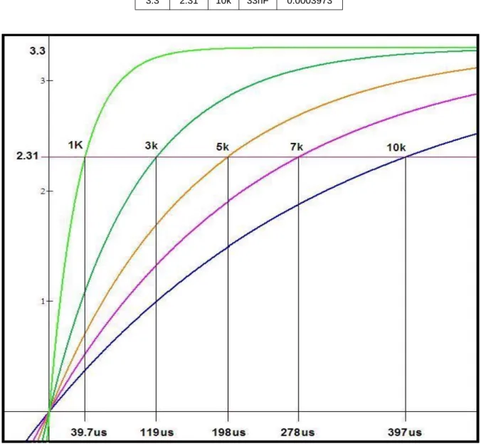
If the MC9RS08 MCU is supplied with 3.3 V then:
V
IH= 0.70 x V
DD= (0.70 x 3.3.) = 2.31 V
Table 1
shows the difference in time using the above with different resistance commercial values.
Figure 3. Charge Curve with Different Resistor Table 1. Time Result According Resistance Values
VDD VIH R C time 3.3 2.31 1k 33nF 3.973E-05 3.3 2.31 3k 33nF 0.0001192 3.3 2.31 5k 33nF 0.0001987 3.3 2.31 7k 33nF 0.0002781 3.3 2.31 10k 33nF 0.0003973
NOTE
The resistor value must not reach 0, or a short circuit can occur.
3.1.1
Code Implementation
The first step is to configure the control pin as output, and setting a low level on it, (0). Then wait for the
RC network to discharge completely;
Pin_Measure:
bset control,PTADD ; Set control pin as Output bclr control,PTAD ; Discharge RC network clr ControlValue
lda #$FE Discharge2:
dbnza Discharge2
The following step is to configure the control pin as input and increment a counter while pin state is 0:
bclr control,PTADD ; Set Control pin as Input measure_pin:
inc ControlValue
brclr control,PTAD,measure_pin; Inc value while pin is in low state rts
The
ControlValuevariable represents the time taken for the capacitor to reach V
IH.
After the pin reaches the high level, we know the approximate position of the potentiometer entered by the
user.
3.2
Temperature Sensor
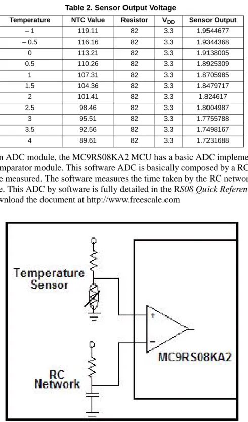
A basic voltage divider with one resistor and one thermoresistor is used to implement the temperature
sensor. The thermoresistor resistance depends on the temperature. For each temperature, we have a
different voltage in the divider. This value is effectively measured with the ADC implemented by software
that uses one resistor, one capacitor, and the analog comparator included in the MC9RS08KA2 MCU.
The voltage divider is composed of the thermoresistor NCP18WB333J03RB and a 82 ohms resistor. It is
better to have a big variation in the output voltage of the sensor with a little variation in the temperature.
The supply voltage of the RC network in this application note is 3.3 V and the output voltage of the sensor
can be calculated with the next equation.
⎟
⎠
⎞
⎜
⎝
⎛
+
=
⎟
⎠
⎞
⎜
⎝
⎛
+
=
82
3
.
3
NTC
NTC
R
NTC
NTC
Vdd
Vout
According to the thermoresistor specifications, the resistor range is between 89.61
Ω
to 116.16
Ω
in a
range of 4 °C to –0.5 °C (
Section Appendix A, “NCP18WB333J03RB Thermistor Range Table
”). With
those values the following data is calculated:
Instead of having an ADC module, the MC9RS08KA2 MCU has a basic ADC implemented by software
using the analog comparator module. This software ADC is basically composed by a RC network and the
analog voltage to be measured. The software measures the time taken by the RC network to reach the
sensor input voltage. This ADC by software is fully detailed in the R
S08 Quick Reference Guide
(RS08QRUG). Download the document at http://www.freescale.com
Figure 4. Sensor Value Input (ADC by Software) Table 2. Sensor Output Voltage
Temperature NTC Value Resistor VDD Sensor Output
– 1 119.11 82 3.3 1.9544677 – 0.5 116.16 82 3.3 1.9344368 0 113.21 82 3.3 1.9138005 0.5 110.26 82 3.3 1.8925309 1 107.31 82 3.3 1.8705985 1.5 104.36 82 3.3 1.8479717 2 101.41 82 3.3 1.824617 2.5 98.46 82 3.3 1.8004987 3 95.51 82 3.3 1.7755788 3.5 92.56 82 3.3 1.7498167 4 89.61 82 3.3 1.7231688
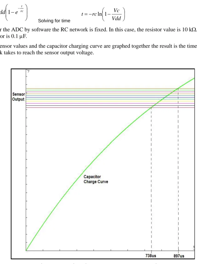
The formula to calculate the time taken for the capacitor to charge is the same as the temperature control
formula :
Solving for time
But, for the ADC by software the RC network is fixed. In this case, the resistor value is 10 k
Ω
. The
capacitor is 0.1
μ
F.
If the sensor values and the capacitor charging curve are graphed together the result is the time the RC
network takes to reach the sensor output voltage.
Figure 5. Capacitor Charge Versus Sensor Output Voltage
⎟⎟
⎠
⎞
⎜⎜
⎝
⎛
−
=
−rc te
Vdd
Vc
1
⎟
⎠
⎞
⎜
⎝
⎛ −
−
=
Vdd
Vc
rc
t
ln
1
Based on the bus speed (8 MHz for this application), it is effective to build a table with the timer value
according the sensor voltage.
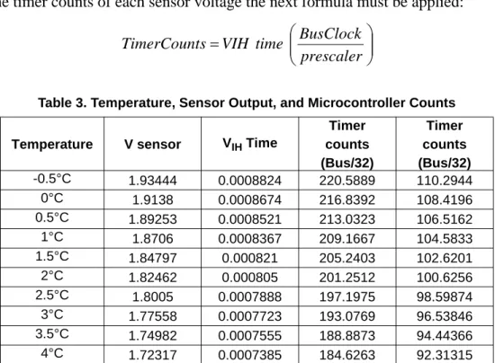
To calculate the timer counts of each sensor voltage the next formula must be applied:
3.2.1
Code Implementation:
ADC_Single_conversion: ; Discharge Capacitor bset 1,PTADD bclr 1,PTAD lda #$FE waste: dbnza wastemov #ACMP_ENABLE,ACMPSC ; ACMP Enabled
mov #MTIM_ENABLE,MTIMSC ; Timer Counter Enabled
wait ; Wait for Analog Comparator Interrupt
bset 4,MTIMSC ; Stop MTIM
lda MTIMCNT ; read counter timer value sta ADCValue ;store counter value mov #MTIM_STOP_RESET,MTIMSC ;Stop and reset counter mov #HIGH_6_13(SIP1), PAGESEL
brset 3, MAP_ADDR_6(SIP1),Conv_OK ; branch if ACMP interrupt arrives bra ADC_Single_conversion
Conv_OK:
mov #ACMP_DISABLED, ACMPSC ; ACMP Disabled, Clear Interrupt flag rts
Table 3. Temperature, Sensor Output, and Microcontroller Counts
Temperature V sensor VIH Time
Timer counts (Bus/32) Timer counts (Bus/32) -0.5°C 1.93444 0.0008824 220.5889 110.2944 0°C 1.9138 0.0008674 216.8392 108.4196 0.5°C 1.89253 0.0008521 213.0323 106.5162 1°C 1.8706 0.0008367 209.1667 104.5833 1.5°C 1.84797 0.000821 205.2403 102.6201 2°C 1.82462 0.000805 201.2512 100.6256 2.5°C 1.8005 0.0007888 197.1975 98.59874 3°C 1.77558 0.0007723 193.0769 96.53846 3.5°C 1.74982 0.0007555 188.8873 94.44366 4°C 1.72317 0.0007385 184.6263 92.31315
⎟⎟
⎠
⎞
⎜⎜
⎝
⎛
=
prescaler
BusClock
time
VIH
s
TimerCount
3.3
Temperature Control Application
The refrigerator’s temperature control has four positions, the range of each one is:
•
Position 4: 0 °C – 1 °C
•
Position 3: 1 °C – 2 °C
•
Position 2: 2 °C – 3 °C
•
Position 1: 3 °C – 4 °C
The control switches on the relay when the temperature is over range. It switches it off when the
temperature reaches the window value.
Because of temperature inertia, the window temperature is 1.5 °C.
Figure 6
shows the window and the
For example, when the temperature position is 1, if the temperature is higher than 4 °C, the relay is closed,
and the refrigerator compressor is on. Next, when the temperature reaches 2.5 °C, the application opens
the relay and the compressor stops.
This guarantees that the temperature is stable for long periods of time between the ranges and, no matter
what; the temperature is never more than 4 °C.
Each temperature limit can be easily changed in the definition part of the main code.
; Variable definitions ; Prescaler /64 TEMP1_ON SET 92 TEMP1_OFF SET 99 TEMP2_ON SET 97 TEMP2_OFF SET 103 TEMP3_ON SET 100 TEMP3_OFF SET 107 TEMP4_ON SET 105 TEMP4_OFF SET 111
The
definition_ONis the value that closes the relay, and
definition_OFFopens the relay. And the
resolution of these values can be adjusted with the timer prescaler.
3.3.1
Code Implementation
;************************************************************** ;* Comparation (Control vs Temp) * ;************************************************************** comparation: lda ControlValue cmp #65 blo Temp1_4 cmp #130 blo Temp2_4 cmp #195 blo Temp3_4
mov #04,ControlValue ; selector = 4 (Coldest) lda ADCValue cmp #TEMP4_ON blo Compresor_ON cmp #TEMP4_OFF bhs Compresor_OFF rts Temp3_4:
mov #03,ControlValue ; selector = 3 (Mid-Low) lda ADCValue cmp #TEMP3_ON blo Compresor_ON cmp #TEMP3_OFF bhs Compresor_OFF rts Temp2_4:
mov #02,ControlValue ; selector = 2 (Mid-High) lda ADCValue cmp #TEMP2_ON blo Compresor_ON cmp #TEMP2_OFF bhs Compresor_OFF rts Temp1_4:
mov #01,ControlValue ; selector = 1 (Hot) lda ADCValue cmp #TEMP1_ON blo Compresor_ON cmp #TEMP1_OFF bhs Compresor_OFF rts Compresor_ON: ; Compresor ON bset output,PTAD rts
Compresor_OFF: ; Compresor OFF
bclr output,PTAD rts
3.4
Schematic
Figure 7. Hardware Schematic
4
Conclusion
This application note shows how to implement a simple on-off control system with a low-end 8-bit
microcontroller.
Appendix A NCP18WB333J03RB Thermistor Range Table
Temp (°C) Resistance (K) -40 1227.263 -35 874.449 -30 630.851 -25 460.457 -20 339.797 -15 253.363 -10 190.766 -5 144.964 0 111.087 5 85.842 10 66.861 15 52.470 20 41.471 25 33.000 30 26.430 35 21.298 40 17.266 45 14.076 50 11.538 55 9.506 60 7.870 65 6.549 70 5.475 75 4.595 80 3.874 85 3.282 90 2.789 95 2.379 100 2.038 105 1.751 110 1.509 115 1.306 120 1.134 125 0.987Appendix B Code Implementation
INCLUDE 'derivative.inc' ; Include derivative-specific definitions ; export symbols XDEF _Startup ABSENTRY _Startup ; Variable declarations ACMP_ENABLE SET $92 ACMP_DISABLED SET $20 MTIM_INIT SET $50 MTIM_ENABLE SET $40 MTIM_STOP_RESET SET $30 MTIM_64_DIV SET $06 FREE_RUN SET $00 DEBUG_MODE SET $00 RUN_MODE SET $01 control SET $04 output SET $05 TEMP1_ON SET 94 TEMP1_OFF SET 100 TEMP2_ON SET 98 TEMP2_OFF SET 104 TEMP3_ON SET 102 TEMP3_OFF SET 108 TEMP4_ON SET 106 TEMP4_OFF SET 112
MODE: EQU DEBUG_MODE ; variable/data section ORG RAMStart ADCValue: DS.B 1 counter DS.B 1 ControlValue DS.B 1 ; code section ORG ROMStart ;************************************************************** ;* MACRO DECLARATION * ;**************************************************************
TRIM_ICS: MACRO ; Macro used to configure the ICS with TRIM mov #$FF,PAGESEL ;change to last page
lda #$FA ; load the content which TRIM value is store tax ; move A content to X
lda ,x ; read D[X]
ENDM ACK_RTI: MACRO
mov #HIGH_6_13(SRTISC), PAGESEL
bset 6,MAP_ADDR_6(SRTISC) ENDM
;************************************************************** ;* Comparation (Control vs Temp) * ;************************************************************** comparation: lda ControlValue cmp #65 blo Temp1_4 cmp #130 blo Temp2_4 cmp #195 blo Temp3_4
mov #04,ControlValue ; selector = 4 (Coldest) lda ADCValue cmp #TEMP4_ON blo Compresor_ON cmp #TEMP4_OFF bhs Compresor_OFF rts Temp3_4:
mov #03,ControlValue; selector = 3 (Mid-Low) lda ADCValue cmp #TEMP3_ON blo Compresor_ON cmp #TEMP3_OFF bhs Compresor_OFF rts Temp2_4:
mov #02,ControlValue ; selector = 2 (Mid-High) lda ADCValue cmp #TEMP2_ON blo Compresor_ON cmp #TEMP2_OFF bhs Compresor_OFF rts Temp1_4:
mov #01,ControlValue; selector = 1 (Hot) lda ADCValue cmp #TEMP1_ON blo Compresor_ON cmp #TEMP1_OFF bhs Compresor_OFF rts
Compresor_ON: ; Compresor ON bset output,PTAD
rts
Compresor_OFF: ; Compresor OFF bclr output,PTAD
rts
;************************************************************** ;* CONFIGURES SYSTEM CONTROL * ;************************************************************** Init_mc:
mov #HIGH_6_13(SOPT), PAGESEL
mov #$E3, MAP_ADDR_6(SOPT) ; Enable STOP mode and COP with long timeout period clr ICSC1 ; FLL is selected as Bus Clock
TRIM_ICS clr ICSC2
bset output,PTADD ; Enable PTA5 as output rts
;************************************************************** ;* Modulus Timer Configuration for ADC * ;************************************************************** MTIM_ADC_Init:
mov #MTIM_64_DIV,MTIMCLK ; Select bus clock as reference, Set prescaler with 64 mov #FREE_RUN,MTIMMOD ; Configure Timer as free running
mov #MTIM_STOP_RESET,MTIMSC rts
;************************************************************** ;* ADC Single Conversion * ;************************************************************** ADC_Single_conversion: ; Discharge Capacitor bset 1,PTADD bclr 1,PTAD lda #$FE waste: dbnza waste ; Start Conversion
mov #ACMP_ENABLE,ACMPSC ; ACMP Enabled, ACMP+ pin active, Interrupt enabled, Rising edges detections
mov #MTIM_ENABLE,MTIMSC ; Timer Counter Enabled
wait ; Wait for Analog Comparator Interrupt (match
signals)
bset 4,MTIMSC ; Stop MTIM
lda MTIMCNT ; read counter timer value sta ADCValue ; store counter value
mov #MTIM_STOP_RESET,MTIMSC ; Stop and reset counter mov #HIGH_6_13(SIP1), PAGESEL
brset 3, MAP_ADDR_6(SIP1),Conv_OK ; branch if ACMP interrupt arrives bra ADC_Single_conversion
Conv_OK:
mov #ACMP_DISABLED, ACMPSC ; ACMP Disabled, Clear Interrupt flag rts
;************************************************************** ;* Control Value * ;************************************************************** Pin_Measure:
bset control,PTADD ; Set control pin as Output bclr control,PTAD ; Discharge RC network clr ControlValue
lda #$FE Discharge2:
dbnza Discharge2
bclr control,PTADD ; Set Control pin as Input measure_pin:
inc ControlValue
brclr control,PTAD,measure_pin; Inc value while pin is in low state rts
;************************************************************** ;* RTI Module Configuration * ;************************************************************** Init_RTI:
mov #HIGH_6_13(SRTISC), PAGESEL
mov #$37, MAP_ADDR_6(SRTISC) ; Enable RTI (1 sec period) rts ;************************************************************** ;* MAIN * ;************************************************************** _Startup: bsr Init_mc bsr Init_RTI
bsr MTIM_ADC_Init ; Configure MITM for ADC module ; Application Loop
mainLoop:
feed_watchdog ; Clear COP timer bsr ADC_Single_conversion ; ADC Conversion
bsr Pin_Measure ; Control Measure jsr comparation ; Comparation
stop ; Enter in STOP mode
ACK_RTI ; Ack for RTI Interrupt
bra mainLoop ;************************************************************** ;* Startup Vector * ;************************************************************** ORG $3FFD JMP _Startup ; Reset
Document Number: AN3409 Rev. 0 01/2007 Home Page: www.freescale.com E-mail: [email protected]
USA/Europe or Locations Not Listed: Freescale Semiconductor
Technical Information Center, CH370 1300 N. Alma School Road
Chandler, Arizona 85224
+1-800-521-6274 or +1-480-768-2130 [email protected]
Europe, Middle East, and Africa: Freescale Halbleiter Deutschland GmbH Technical Information Center
Schatzbogen 7 81829 Muenchen, Germany +44 1296 380 456 (English) +46 8 52200080 (English) +49 89 92103 559 (German) +33 1 69 35 48 48 (French) [email protected] Japan:
Freescale Semiconductor Japan Ltd. Headquarters ARCO Tower 15F 1-8-1, Shimo-Meguro, Meguro-ku, Tokyo 153-0064 Japan 0120 191014 or +81 3 5437 9125 [email protected] Asia/Pacific:
Freescale Semiconductor Hong Kong Ltd. Technical Information Center
2 Dai King Street Tai Po Industrial Estate Tai Po, N.T., Hong Kong +800 2666 8080
For Literature Requests Only:
Freescale Semiconductor Literature Distribution Center P.O. Box 5405
Denver, Colorado 80217 1-800-441-2447 or 303-675-2140 Fax: 303-675-2150
implementers to use Freescale Semiconductor products. There are no express or implied copyright licenses granted hereunder to design or fabricate any integrated circuits or integrated circuits based on the information in this document.
Freescale Semiconductor reserves the right to make changes without further notice to any products herein. Freescale Semiconductor makes no warranty, representation or guarantee regarding the suitability of its products for any particular purpose, nor does Freescale Semiconductor assume any liability arising out of the application or use of any product or circuit, and specifically disclaims any and all liability, including without limitation consequential or incidental damages. “Typical” parameters that may be provided in Freescale Semiconductor data sheets and/or specifications can and do vary in different applications and actual performance may vary over time. All operating parameters, including “Typicals”, must be validated for each customer application by customer’s technical experts. Freescale Semiconductor does not convey any license under its patent rights nor the rights of others. Freescale Semiconductor products are not designed, intended, or authorized for use as components in systems intended for surgical implant into the body, or other applications intended to support or sustain life, or for any other application in which the failure of the Freescale Semiconductor product could create a situation where personal injury or death may occur. Should Buyer purchase or use Freescale Semiconductor products for any such unintended or unauthorized application, Buyer shall indemnify and hold Freescale Semiconductor and its officers, employees, subsidiaries, affiliates, and distributors harmless against all claims, costs, damages, and expenses, and reasonable attorney fees arising out of, directly or indirectly, any claim of personal injury or death associated with such unintended or unauthorized use, even if such claim alleges that Freescale Semiconductor was negligent regarding the design or manufacture of the part.
Freescale™ and the Freescale logo are trademarks of Freescale Semiconductor, Inc. All other product or service names are the property of their respective owners.
© Freescale Semiconductor, Inc. 2007. All rights reserved.
RoHS-compliant and/or Pb-free versions of Freescale products have the functionality and electrical characteristics as their non-RoHS-compliant and/or non-Pb-free counterparts. For further information, see http://www.freescale.com or contact your Freescale sales representative.
For information on Freescale’s Environmental Products program, go to