Single-input Multiple-output Tunable Log-domain
Current-mode Universal Filter
Pipat PROMMEE, Kobchai DEJHAN
Department of Telecommunications Engineering, Faculty of Engineering, King Mongkut’s Institute of Technology Ladkrabang, Bangkok 10520, Thailand
[email protected] Abstract. This paper describes the design of a
current-mode single-input multiple-output (SIMO) universal filter based on the log-domain filtering concept. The circuit is a direct realization of a first-order differential equation for obtaining the lossy integrator circuit. Lossless integrators are realized by log-domain lossy integrators. The proposed filter comprises only two grounded capacitors and twenty-four transistors. This filter suits to operate in very high frequency (VHF) applications. The pole-frequency of the proposed filter can be controlled over five decade fre-quency range through bias currents. The pole-Q can be independently controlled with the pole-frequency. Non-ideal effects on the filter are studied in detail. A validated BJT model is used in the simulations operated by a single power supply, as low as 2.5 V. The simulation results using PSpice are included to confirm the good performances and are in agreement with the theory.
Keywords
Log-domain filtering, very high frequency, low-voltage, electronically-controlled, universal filter.
1.
Introduction
In 1979, Adams introduced a novel class of continu-ous-time filters called log-domain filters which externally are linear systems, yet internally are nonlinear [1]. This class originates from the companding concept (compress and expand) of log-domain circuits. Input linear current is initially converted to a compressed voltage, and then proc-essed by the log-domain core block. The comprproc-essed out-put voltage is converted to a linear current to preserve the linear operation of the whole system. The compression and expansion of the corresponding signals are based on the logarithmic/exponential voltage–current relationship of a bipolar transistor. Log-domain circuits are useful build-ing blocks for realizbuild-ing high-performance current-mode analogue signal processing systems.
In 1993, Frey introduced a general method for syn-thesizing log-domain filters of arbitrary order using a state-space approach [2], [3]. Frey also presented a highly
modular technique for implementing such filters from a simple building block comprising a bipolar current mirror whose emitters are driven by complementary emitter fol-lowers. Log-domain filters based on instantaneous com-panding [4]–[7] and these circuits are both theoretical and technological interested, since they have potentially offered high-frequency operation, tunability, and extended dy-namic range under low power supply voltages [8]–[20].
A biquadratic filter is a basic second-order function block for realizing high-order filter functions. The multi-function filter circuit based on a biquadratic multi-function has been designed and developed for over four decade years [21]-[31]. The single output OTA (SO-OTA) was used in realizing the voltage-mode biquad filters based on a two-integrator loop structure in [22]. The circuit in [23] suf-fered from using a large number of OTAs. Other filters have been introduced based on multiple current output OTAs and grounded capacitors. The two-integrator loop current-mode filters based on lossless and lossy integrators (two OTAs and two grounded capacitors) were proposed in [24], [25]. The concept of component minimization for realizing the universal biquad filters has also been intro-duced. However, it cannot adjust pole-Q (Q0) without
af-fecting the pole-frequency (0). Two-integrator loop
struc-tures using multiple current output OTAs and grounded capacitors have been introduced in [26], [27]. Summations of feedback of zeros to the rational function for realizing the filter were introduced in [28]-[31]; however, some circuits require too many active devices or excessive pas-sive components and others cannot adjust the pole-Q with-out affecting the pole-frequency. The programmable zeros are obtained by either bias current or analogue switches. However, a performance limitation of the OTA including low bandwidth, high power supply and large die area can be observed.
Other active elements in the family of current convey-ors including CCII [32-34], DVCC [35], DDCC [36] CCCII [37-40] and DXCCII [39] have been widely used for filter realization. However, the voltage and current tracking errors are the main problems of current conveyors. Active-only components based on OPAMP gain-bandwidth and OTAs have also been used in implementing the univer-sal filter [42-43].
Unfortunately, several filters based on active building blocks (ABB) [21-43] are suitable for several megahertz range that they cannot operate in very high frequency ap-plications. The narrow tunable range is a problem of ABB-based filer. Owing to log-domain filtering concept, it is including the following potential capabilities: low-voltage, high-frequency operation and wide electronic tunability. The above mentioned problems of ABB can be solved. In this paper, a high-frequency single-input multiple-output (SIMO) biquad universal filter is realized based on log-domain integrators loop. It is suitable for wireless systems [9] and high-frequency applications such as video signal processing, magnetic disk read channel, sensor signal con-ditioning [44]-[48]. The proposed circuit possesses the following features:
1) The configuration is realized by using minimum num-ber of active and passive components.
2) Use of grounded capacitors, thus it is suitable for inte-gration.
3) Orthogonal electronic tunability between 0 and Q0.
4) High-frequency operation is achieved based on the log-domain concept with wide electronic tunability and low-power supplies features.
5) High-output impedance, thus it enables interconnec-tion to the succeeding current-mode circuits.
A + + s B -1 CFig. 1. Lossless integrator realized from a lossy integrator.
2.
Theory and Principle
2.1
Lossless Integrator Realized by Lossy
Integrator
Lossless and lossy integrators perform the same func-tion as dependent building blocks, but a lossy integrator performs as a first order low-pass filter. A lossy integrator can be transformed to a lossless integrator or vice versa [19]. This paper uses the realization of a lossless integrator by transforming a lossy integrator. The inverting and non-inverting lossless integrators in Fig. 1 can easily be ob-tained by the transfer function at different nodes.
C s A s s
(1)
B s A s s
(2)2.2
Low-Pass Biquad Structure Realization
The inverting biquadratic low-pass (LP) function for synthesizing the system can generally be described by
2 Z s AB W s s skA AB . (3)The above equation can be rewritten in terms of lossless integrators as follows:
B A
A Z s W s Z s kZ s s s s . (4)
A s B sFig. 2. Block diagram of a two-integrator loop filter.
Based on Fig. 2, other transfer functions of different nodes can, respectively, be obtained.
2 2 X s s W s s skA AB , (5)
2 Y s skA W s s skA AB . (6)
2.3
Log-domain Lossy Integrator Based on
Translinear BJT
Fig. 3(a) shows a log-domain filtering scheme based on a translinear type-B (balance) cell [49] which is called
(a)
(b)
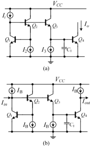
Fig. 3. Log-domain inverting lossy integrator (a) analytic structure, (b) practical structure.
a log-domain lossy integrator. Assuming that each transis-tor has an ideal exponential characteristic (base-current is neglected) and using Kirchhoff’s current law (KCL), the base-emitter voltage relations can be written as
1 2 3 4 0
be be be be
V V V V . (7)
The collector current of the transistor is given by
exp be c S T V I I V (8)
where the different terms have their usual meaning. Now, applying the translinear principle (TLP) [50] to Q1-Q4
gives
1 2 3 4 C C C C
I I I I . (9.1)
If IC1 = Ii, IC2 = I2 and IC4 = IO, then (9.1) becomes 2 3
i C O
I I I I . (9.2)
Collector current of Q3 can be expressed as 3 3 1 1
C C
I I C V . (10)
The derivative of the voltage across the capacitor C1 is 1 1 C T out T O C O O dV V dI V I V dt I dt I . (11)
The derivative of the output current based on (8) yields
1 1 1 exp O S C C O O C T T T dI I V dV I I V dt V V dt V . (12)
Substituting (10), (11) and (12) into (9), we get
1 2 3 O T i O O C I V I I I I I . (13) Suppose that we define the currents I2 = I3 = I, then (13)
becomes 1 O T i O C I V I I I . (14)
By taking the Laplace transform into (14) and rear-ranging, the transfer function of the circuit of Fig. 3(a) in the s-domain is
1 1 1 O i T I s H s I s s C V I . (15)It is seen from (15) that H(s) corresponds to the trans-fer function of a lossy integrator, and that the natural fre-quency can be controlled by the bias current I.
Considering the direction of input and output currents in Fig. 3(a), it can be seen that this structure can easily produce the non-inverting lossy integrator function. The constant currents Ii, I2 and I3 are, respectively, replaced by
Iin+IB, IB and IB as shown in Fig. 3(b). The current output
Iout requires the bias current IB for offset cancellation. The final current output of Fig. 3(b) is obtained as
11
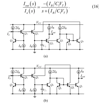
out B T a B T I s I C V I s s I C V . (16) (a) (b)Fig. 4. Log-domain lossless integrator realized using a lossy integrator: (a) Inverting, (b) non-inverting.
As mentioned in Section 2.1, lossless integrator can be realized by feeding back the output current to the input. The inverting and non-inverting lossless integrators are, respectively, depicted in Fig. 4(a) and (b) and their transfer functions can be expressed as
1 out B a T I s I I s sC V , (17)
1 out B b T I s I I s sC V . (18)Fig. 5. Tunable translinear inverting current-gain.
2.4
Translinear Current-gain
The current-gain in this paper is facilitated by the translinear concept [49] as shown in Fig. 5, which provides the current output as a multiplier and divider. The bias currents are replaced and applied the input current (Iin) then the linear current output function can be obtained based on the translinear principle as
2 3 in in O I I kI I I . (19)
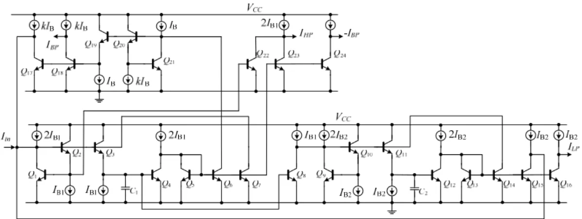
Fig. 6. Single-input multiple-output tunable log-domain current-mode universal filter.
It is found that the current gain can be adjusted by the ratio of bias currents I2 and I3.
3.
Log-domain Current-mode
Universal Filter
The proposed filter as shown in Fig. 6 is realized based on the two- integrator loop structure, where the
pole-Q is tunable by adjusting the current-gain block (k). It is straightforward to show that the output current of LP, BP and HP are given by
2 1 2 1 2 B B T LP in I I C C V I I D s , (20)
1 1 B T BP in s kI C V I I D s , (21)
2 HP in I s I D s (22) where
2
2 1 1 1 2 1 2 B T B B T D s s s kI C V I I C C V .Note that the proposed circuit can easily realize other two types of standard transfer functions by summing the particular outputs, which are summarized below.
i) The BR response can be realized by summing of HP and LP output currents (IHP + ILP).
ii) The AP response can be realized by summing of HP, LP and negative BP output currents (IHP + ILP + (-IBP)).
The pole-frequency (0) and pole-Q (Q0) can be
expressed as 1 2 0 1 2 1 B B T I I V C C
, (23) 2 1 0 1 2 1 B B I C Q k I C . (24)The parameters IBi, VT and k represent the bias cur-rents, thermal voltage ( 26mV at room temperature) and current-gain, respectively. From (23) and (24), it is seen that the pole-frequency can be linearly tuned by adjusting the bias currents (IBi), while the pole-Q can be electroni-cally tuned by adjusting the current gain building block (k) without affecting the frequency. Note that the pole-frequency is directly influenced by temperature (thermal voltage (VT)). This effect can be reduced by using the com-pensated bias currents.
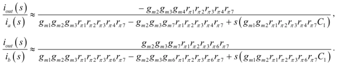
The current biasing circuit of the proposed filter is shown in Fig. 7, which is based on positive and negative
QB4 QB3 VCC QB2 QB1 IB 2IB1 IB1 IB2 IB1 IB1 IB2 IB2 QB6 QB13 QB14 QB16 QB22 QB26 kIB VCC Replace for tunable pole-Q Extra Biasing kIB QB9 QB9 QB33 kIB IB2 kIB kIB QB20 QB23 QB24 QB5 IB1 IB QB7 QB8 2IB1 QB11 QB12 2IB2 QB21 QB19 2IB2 QB15 QB18 IB kIB kIB QB31 QB30 QB23 QB24 QB10 QB27 QB28 QB29 QB32 QB25 2IB1 QB17
1 2 3 1 2 3 4 7 2 23 37 14 21 32 43 74 7
1 2 1 2 3 4 7 1
out m m m a m m m m m m m m i s g g g r r r r r i s g g g r r r r r g g g r r r r r s g g r r r r r C , (25.1)
1 2 3 1 2 3 6 7 22 33 671122336677
1 2 1 2 3 6 7 1
out m m m b m m m m m m m m i s g g g r r r r r i s g g g r r r r r g g g r r r r r s g g r r r r r C . (25.2)current mirrors. For Q0 = 1, the positive and negative bias
currents can be tuned simultaneously by single bias current
IB. The general current biasing circuit contains transistors
QB1-QB28 that are implemented to the 18 bias currents. For
tunable pole-Q, QB9, QB23,QB24 are removed and replaced
by the extra biasing circuit. Pole-Q can be independently tuned by adjusting the extra bias current kIB and the pole-frequency is tuned by bias current IB.
Fig. 8. Simple small signal of BJT transistor.
4.
Non-idealities Studies
Log-domain filter suffers from transistor nonideali-ties. The study of nonideal log-domain filters is compli-cated in the fact that the non-linear logarithmic-exponential operations inherent the circuit result in transcendental equations. This paper derives equations describing the non- ideal characteristics of the log-domain circuit as a con-sequence of the deviations in the nonideal parameters. This section shows the effects of the transistor parasitic in Fig. 8 based on a small-signal model using transconductance (gm = IC / VT), base-emitter resistance (r), base-emitter
capacitance (C), and base-collector capacitance (Cµ). We
assume that the other parasitic capacitances are very small and the impedance of the collector-emitter (rce) is high. Physical parameters such as area mismatch and early volt-age are also discussed.
4.1
Influences of Parasitic Resistance (
r
)
This qualitative analysis shows that the transistor non-idealities, including the parasitic resistances and parasitic capacitances, are the sources of error within log-domain circuits. Finite beta and base-emitter resistance have gener-ally been identified as the most problematic error sources at low frequencies [51].Parasitic base-emitter resistance (r) is a limitation of
the translinear circuit accuracy at high-frequencies. From the small-signal model of a bipolar transistor, when the parasitic capacitances are neglected, the effect of r to
inverting and non-inverting lossless integrator transfer function is, respectively, described by(25.1) and (25.2). They can be simplified and rewritten as
1 2 3 2 2 3 37 4
1 2 1
out m m m a m m m m m m m m i s g g g i s g g g g g g s g g C ,(26.1)
1 2 3 22 33 67
1 2 1
out m m m b m m m m m m m m i s g g g i s g g g g g g s g g C . (26.2)From (26), it can be seen that the both types of loss-less integrators has no effects from the parasitic resistance (r). Moreover, it can be seen that the transistor Q1 and Q7
should be matched for inverting lossless in integrator. Likewise, the transistor Q1 and Q6 should be matched for
inverting lossless in integrator. The function of lossless integrators can be well operated according to the theoreti-cal aspect.
4.2
Influences of Parasitic Capacitance (
C
and
C
µ)
Parasitic base-emitter capacitance (C) is also a major
limitation to translinear circuit accuracy, particularly at high-frequencies. Using the small-signal model of the bi-polar transistor with parasitic capacitances, the effect of C
to inverting lossless integrator transfer function can be approximated in (27.1) and (27.2).
Assuming that the transconductances of the transis-tors are matched, the transfer functions in (27.1) and (27.2) become
1 7 4 1
out m a i s g i s s C C C C , (28.1)
1 7 4 2 3
2 out m a i s g i s s C C C C C . (28.2)
1 2 3 2 3 7 1 2
1 3 7 2 34
4 1 3 2 2 7 3 3 7
2 1
out m m m a m m m m m m m m m m m m m m i s g g g i s g g g g g g s g g C C C C g g C g g C g g C C , (27.1)
1 2 3 2 3 7 1 2
1 7 4
2 31 43 1 2 3
2 3 7
3 7 1 out m m m a m m m m m m m m m m m m m m i s g g g i s g g g g g g s g g C C C g g C g g C C C g g C , (27.2)
1 2 3 2 3 6 1 2
1 3 62 3 7
7 1 3 2 2 6 3 3 6
1 2
out m m m b m m m m m m m m m m m m m m i s g g g i s g g g g g g s g g C C C C g g C g g C g g C C , (29.1)
1 2 3 2 3 6 1 2
1 7 62
3 17 3 1 3 6 1 2 3
2 3 6
out m m m b m m m m m m m m m m m m m m i s g g g i s g g g g g g s g g C C C g g C g g C g g C C C . (29.2)Similarly, parasitic base-collector capacitance (Cµ) is also a major limitation to translinear circuit accuracy. The effect of the base-collector capacitance to the non-inverting lossless integrator transfer function is given by (29.1) and (29.2).
Again assuming that the transconductances of the transistors are matched, the transfer functions in (29.1) and (29.2) become
1 6 7 1
out m b i s g i s s C C C C , (30.1)
1 2 3 7 2 6
out m b i s g i s s C C C C C . (30.2)From (30.1) and (30.2), it is seen that the parasitic capacitances Ci and Cµi produce a small deviation in the
frequency response in lossless integrators. The natural frequency is of the form 0 = I / CVT, high frequency
operation can be realized by increasing the bias current or reducing the capacitance. To maintain the low-power, the bias currents are kept at a lower level and the integrating capacitance is increased. To prevent significant distortion, the selected capacitance C should be
5
i i
CC C . (31)
Note that there are high-order poles (2nd and 3rd order
poles) which affect to higher frequencies than the operation frequency of the filter. These poles can be neglected.
4.3
Influences of Area Mismatches
Emitter area mismatches cause variations in the satu-ration current (IS) between transistors. Taking into account the emitter area, (14) can be rewritten as
1 out T in out C I V kI I I (32) where 3 4 3 4 1 2 1 2 S S S S I I A A I I A A .
From (32), it is clear that the area mismatches introduce only a change in the proportionality constant or DC gain of the low-pass filter without affecting the linearity or the time constant of the circuit. The gain error can be easily compensated by adjusting one of the DC bias currents.
4.4
Influences of Early Effect
Early effect (base-width modulation) causes the col-lector current error by the colcol-lector-emitter and
base-col-lector voltages. Considering the variation of colbase-col-lector- collector-emitter voltage, the collector current can be written as
Ic = (1 + Vce / VA)ISexp(Vbe / VT), where VA is the forward-biased early voltage. An analysis of the integrator shows the early effect with a scalar error to the DC gain of the circuit as in the case of the area mismatches. Since Vce has been signal-dependent, the device base-width modulation also introduces distortion. Since the voltage swings in the current-mode companding circuits have been very low (Vbes), the early effect is not a major source of distortion.
4.5
Influences of the Bias Currents
The proposed log-domain filter employs bias currents which are provided by positive and negative current sources. The positive (IBP) and negative (IBN) current sources are respectively replaced by positive and negative current mirrors in Fig. 7. The transconductance of the tran-sistors are controlled by the particular bias currents. Posi-tive and negaPosi-tive current mirror errors which affect the filter performances are considered.
Based on the configuration of lossless integrators in Fig. 4, the positive and negative bias currents are given by
IBP = PIB and IBN = NIB, where P and N represent the
current gains of the positive and negative current mirrors, respectively. It can be seen that if the transconductances
gm1= gm4= gm5= gm6= gm7= gmp and gm2= gm3= gmn, then (26.1) and (26.2) become
1 1 out mn N B a T i s g I i s sC sV C , (33.1)
1 1 out mn N B b T i s g I i s sC sV C . (33.2)From the translinear current gain in Fig. 5, current output has no effects from the current gain of current mir-rors. It can be seen that the gain of current mirrors affect only the lossless integrator configurations. Re-analyzing Fig. 6, the denominator can be rewritten as
2
2 2 21 1 2
n N B T N B T
D s s s kI C V I C C V . (34) The non-ideal pole-frequency (0n) and pole-Q (Q0n)
can be expressed as 0 1 2 1 N B n T I V C C , (35) 1 0 2 1 n C Q k C . (36)
It is evident from (35) that slight deviation only in the pole-frequency is caused due to the errors of the bias cur-rent IBN. To reduce these errors, accurate current mirrors as well as cascode current mirrors are required. Note that the pole-Q has no effects from the error of bias currents.
.MODEL C12TYP NPN
+ (IS=7.40E-018 BF=1.00E+002 BR=1.00E+000 NF=1.00E+000 + NR=1.00E+000 TF=6.00E-012 TR=1.00E-008 XTF=1.00E+001 + VTF=1.50E+000 ITF=2.30E-002 PTF=3.75E+001 VAF=4.50E+001 + VAR=3.00E+000 IKF=3.10E-002 IKR=3.80E-003 ISE=2.80E-016 + NE=2.00E+000 ISC=1.50E-016 NC=1.50E+000 RE=5.26E+000 + RB=5.58E+001 IRB=0.00E+000 RBM=1.55E+001 RC=8.09E+001 + CJE=3.21E-014 VJE=1.05E+000 MJE=1.60E-001 CJC=2.37E-014 + VJC=8.60E-001 MJC=3.40E-001 XCJC=2.30E-001 CJS=1.95E-014 + VJS=8.20E-001 MJS=3.20E-001 EG=1.17E+000 XTB=1.70E+000 + XTI=3.00E+000 KF=0.00E+000 AF=1.00E+000 FC=5.00E-001)
(a) NPN-HSB2 provided by ST Microelectronics .model HFA3128 PNP
+ (IS=1.027E-16 XTI=3.000E+00 EG=1.110E+00 VAF=3.000E+01 + VAR=4.500E+00 BF=5.228E+01 ISE=9.398E-20 NE=1.400E+00 + IKF=5.412E-02 XTB=0.000E+00 BR=7.000E+00 ISC=1.027E-14 + NC=1.800E+00 IKR=5.412E-02 RC=3.420E+01 CJC=4.951E-13 + MJC=3.000E-01 VJC=1.230E+00 FC=5.000E-01 CJE=2.927E-13 + MJE=5.700E-01 VJE=8.800E-01 TR=4.000E-09 TF=20.05E-12 + ITF=2.001E-02 XTF=1.534E+00 VTF=1.800E+00 PTF=0.000E+00 + XCJC=9.000E-01 CJS=1.150E-13 VJS=7.500E-01 MJS=0.000E+00 + RE=1.848E+00 RB=3
(b) PNP-HFA3128 provided by Intersil
Tab. 1. Bipolar model parameter of used for SPICE simula-tion.
5.
Simulation Results
In order to verify the operation of the circuit topology of Fig. 6, a filter with a single input and four outputs is designed. The power supply voltage (VCC) is assigned to 2.5 V and the bias current IB is varied from 0.01 A to 1,000 A at room temperature. To prevent the parasitic effects of the filter, capacitors are chosen to be much larger than C+ 5Cµ by assigning C1 = C2 = 50 pF. The
high-speed bipolar technology (HSB2) provided by ST Micro-electronics [52] is used in the simulations. The transistor model is listed in Tab. 1.
Fig. 9. LP, HP and BP filter characteristics at IB = 100 µA, C = 50 pF.
The amplitude response of LP, BP, HP and BR filters based on Fig. 6 with IB = 100 A and C1 = C2 = 50 pF is
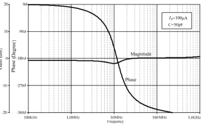
shown in Fig. 9. Fig. 10 illustrates amplitude and phase responses simulation around 10 MHz of AP filter.
Fig. 10. AP filter characteristics.
Fig. 11 shows the tunable pole-frequency of BP filter by varying the current bias (IB) from 0.01 A to 1,000 A. A wide range of pole-frequency tuning is obtained from 1 kHz to 100 MHz.
Fig. 11. Tunable BP frequency response by using various bias currents.
A comparison of the magnitude response between the simulated LP filter and the ideal Butterworth LP function in (20) is exhibited in Fig. 12. Slight difference in fre-quency responses of simulated and ideal LP functions is observed due to the effects of parasitic capacitances at high frequency which was discussed in Section 4.2.
Fig. 12. Comparison between the simulation results and theoretical results.
The pole-Q can be electronically tuned (at 10 MHz) from 1 to 16 by assigning IB= 100 µA and varying the current bias
kIB from 6.25 µA to 100 µA, and is shown in Fig. 13.
Fig. 13. Pole-Q tuning characteristics for Q = 1, 2, 4, 8 and 16.
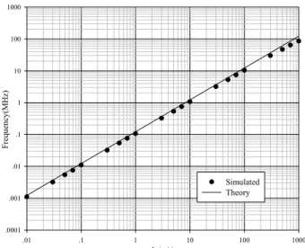
Frequency response of the proposed filter for a time-domain signal can be investigated by assigning the BP pole-frequency at 100 MHz (IB= 1,000 µA). The different frequencies of sinusoidal input (10 MHz, 100 MHz and 1 GHz) are applied based on 200 µAp-p. The linear tunability range of frequency response from 1 kHz to 100 MHz based on various bias currents from 0.01 µA to 1,000 µA and C = 50 pF is illustrated in Fig. 14.
IB(uA) .01 .1 1 10 100 1000 Fr equency(M H z) .0001 .001 .01 .1 1 10 100 1000 Simulated Theory
Fig. 14. Tunable frequency response by using various bias currents.
The different frequency output currents of BP filter (f0= 100 MHz) are shown in Fig. 15(a)-(c). It can be seen
that the highest current output (Fig. 15(b)) is obtained at 100 MHz.
Noise analysis at different outputs of the proposed filter is shown in Fig. 16. Low-noise values of LP, BP and HP filters are obtained lower than 133pV H.
Tab. 2 illustrates a comparison of the proposed uni-versal filter with previous uniuni-versal filters. The first 2 pa-pers are based on log-domain concept [16], [17]. The rest [27], [35], [36], [38], [41] and [43] are based on different active building blocks (ABB). Note that the existing uni versal filters have at least drawbacks of requiring dual sup-
(a)
(b)
(c)
Fig. 15. Time domain response of BP filter based on
f0 = 100 MHz: (a) input = 10 MHz, (b) input = 100 MHz,
(c) input = 1 GHz. Frequency 100Hz 1.0KHz 10KHz 100KHz 1.0MHz 10MHz 100MHz 1.0GHz 128pV 130pV 132pV 134pV LPF BPF HPF
Fig. 16. Noise analysis of proposed filter based on f0 = 10 MHz. plies and many transistors. Although, the class-AB log-domain filter [16] provides quite good performance in frequency response but suffers by many transistors, four capacitors, current splitter and complex structure. Another log-domain SIMO and MISO filters [17] use low power supply but suffer by high number of components (BJT and MOS), extra voltage sources and complex structure. The ABB-based filters [27], [35], [36], [38], [41] and [43] can
operate only in low megahertz range with narrow tunable ranges. The proposed filter based on +2.5 V single supply offers the following features: high frequency, linear wide-range tunability, simply structure and low-component count. Filter Power supply Tunable frequency range Number of transistors Use of resistor Mode of operation [16] +3 V 149 MHz 47 No CM [17] +1.5 V 10 MHz 58/52 No CM [27] ±5 V < 10 MHz 47 No CM [35] ±2.5 V < 22.5 MHz 62 No CM [36] ±1.25 V < 10 MHz 36 Yes VM [38] ±2.5 V < 10 MHz 56 No CM [41] ±1.25 V < 10 MHz 70 No CM [43] ±2.5 V < 5 MHz 98 No CM/VM Proposed +2.5 V 1k-100 MHz 24 No CM
Tab.2. Comparison of previous universal filters with the proposed filter.(Remark: Some preliminary results of the paper have appeared in [20].)
6.
Conclusion
A novel low-voltage single-input multiple-output cur-rent-mode universal filter based on log-domain concept has been presented. The proposed filter is realized based on two lossless integrators loop concept which consists of two lossless integrator, a current gain and additional transistors for obtaining outputs. Each lossless integrator contains only 7 transistors and a grounded capacitor which is real-ized by transforming a lossy integrator. Five types of stan-dard filter functions with high impedance output currents are produced based on a 2.5 V power supply. The proposed filter consists of 24 transistors and 2 grounded capacitors. A wide range of tunable pole-frequency is obtained from 1 kHz to 100 MHz by varying IB from 0.01 A to 1000 A. The pole-Q can be tuned without affecting the pole-fre-quency.
Acknowledgement
The authors would like to express their sincere thanks to Dr. M.N.S. Swamy of Concordia University, Canada and Mr. Natapong Wongprommoon and anonymous re-viewers for their very helpful comments and suggestions, which have significantly improved the manuscript.
References
[1] ADAMS, R. W. Filtering in the log domain. In 63rd AES Conv. Los Angeles (CA), May 1979, preprint 1470.
[2] FREY, D. R. Log-domain filtering: An approach to current-mode filtering. Proc. IEE, part G, 1993, vol. 140, no. 6, p. 406–416. [3] FREY, D. R. Exponential state-space filters: a generic current
mode design strategy. IEEE Trans Circuits Systems-I, 1996, vol. 43, p. 34–42.
[4] SEEVINCK, E. Companding current-mode integrator: A new circuit principle for continuous-time monolithic filters. Electron. Lett., 1990, vol. 26, no. 24, p. 2046–2047.
[5] TSIVIDIS, Y. On linear integrators and differentiators using instantaneous companding. IEEE Trans. Circuits Syst. II, Aug. 1995, vol. 42, p. 561–564.
[6] TSIVIDIS, Y. General approach to signal processors employing companding. Electron. Lett., 1995, vol. 31, no. 18, p. 1549–1550. [7] TSIVIDIS, Y. Instantaneously companding integrators. In Proc.
IEEE Int. Symp. Circuits Syst. (ISCAS’97). Hong-Kong, 1997, vol. 1, p.477–480.
[8] FREY, D. R. A 3.3 V electronically tunable active filter usable to beyond 1 GHz. In Proc. IEEE Int. Symp. Circuits Syst. (ISCAS’94). London (U.K.), 1994, vol. 5, p. 493–496.
[9] FREY, D. R. On log-domain filtering for RF applications. IEEE J. Solid-State Circuits, Oct. 1996, vol. 31, p. 1468–1475.
[10] FREY, D. R. An adaptive analog notch filter using log-filtering. In
Proc. IEEE Int. Symp. Circuits Syst. (ISCAS’96). Atlanta (GA), 1996, vol. 1, p. 297–300.
[11] KIRCAY, A., CAM, U. A novel log-domain first-order multifunction filter. ETRI Journal, June 2006, vol. 28, no. 3. [12] DRAKAKIS, E. M., PAYNE, A. J., TOUMAZOU, C. Log-domain
filtering and the Bernoulli cell. IEEE Trans. Circuits Syst. I, May 1999, vol. 46, no. 5, p. 559–571.
[13] PSYCHALINOS, C. On the transposition of Gm-C filters to DC stabilized log-domain filters. Int. J. Circ. Theor. Appl., 2006, no. 34, p. 217–236.
[14] PSYCHALINOS, C. Realization of log-domain high-order transfer functions using first-order building blocks and complementary operators. Int. J. Circ. Theor. Appl., 2007, vol. 35, p. 17–32. [15] PSYCHALINOS, C. Log-domain linear transformation filters
revised- improved building blocks and comparison results. Int. J. Circ. Theor. Appl., 2008, vol. 36, p. 119–133.
[16] TOLA, A. T., ARSLANALP, R., YILMAZ, S. S. Current mode high-frequency KHN filter employing differential class AB log domain integrator. International Journal of Electronics and Communications (AEÜ), 2009, vol. 63, no. 7, p. 600-608.
[17] PSYCHALINOS, C. Log-domain SIMO and MISO low-voltage universal biquads. Analog Integrated Circuits and Signal Proc-essing, 2011, vol. 67, no. 2, p. 201–211.
[18] PROMMEE, P., SRA-IUM, N., DEJHAN, K. High-frequency log-domain current-mode multiphase sinusoidal oscillator. IET Cir-cuits Devices Syst., 2010, vol. 4, no. 5, p. 440–448.
[19] PROMMEE, P., PRAPAKORN, N., SWAMY, M.N.S. Log-do-main current-mode quadrature sinusoidal oscillator. Radioengi-neering, 2011, vol. 20, no.3, p. 600-607.
[20] PROMMEE, P., SOMDUNYAKANOK, M., ANGKEAW, K., DEJHAN, K. Tunable current-mode log-domain universal filter. In
Proc. of IEEE ISCAS 2010. Paris (France), May 29-June 2, 2010. [21] KERWIN, W. J., HUELSMAN, L. P., NEWCOMB, R. W.
State-variable synthesis for insensitive integrated circuit transfer func-tion. IEEE Trans. Solid-state Circuits, 1967, vol. SC-2, p. 87-92. [22] SANCHEZ-SINENCIO, E., GEIGER, R. L.,
filter structures. IEEE Trans. Circuits and Syst., 1988, vol. 35, p. 936-946.
[23] WU, J., XIE, C. New multifunction active filter. Int. J. Electron., 1993, vol. 74, p. 235-239.
[24] CHANG, C. New multifunction OTA-C biquads. IEEE Trans. Circuits and Syst., 1999, vol. 46, p. 820-824.
[25] CHANG, C., PAI, S. Universal current-mode OTA-C biquad with the minimum components. IEEE Trans. Circuits and Syst, 2000, vol. 47, p. 1235-1238.
[26] CHANG, C., AL-HASHIMI, B. M., ROSS, J. N. Unified active fil-ter biquad structure. IEE Proc., part G, 2004, vol. 151, p. 273-277. [27] PROMMEE, P., PATTANATADAPONG, T. Realization of tun-able pole-Q current-mode OTA-C universal filter. Circuits, Sys-tems, and Signal Processing, Oct. 2010, vol. 29, no. 5.
[28] SUN, Y., FIDLER, J. K. Structure generation of current-mode two integrator loop dual output-OTA grounded capacitor filters. IEEE Trans. Circuits and Syst., 1996, vol. 43, p. 659-663.
[29] CHANG, C., AL-HASHIMI, B. M. Analytical synthesis of current-mode high-order OTA-C filters. IEEE Trans. Circuits and Syst., 2003, vol. 50, p. 1188-1192.
[30] TU, S. H., CHANG, C., ROSS, J. N., SWAMY, M. N. S. Analytical synthesis of current-mode high-order single-ended-input OTA and equal-capacitor elliptic filter structures with the minimum number of components. IEEE Trans. Circuits and Syst. I, 2007, vol. 54, p. 2195-2210.
[31] AL-HASHIMI, B. M., DUDEK, F., MONIRI, M., LIVING, J. Integrated universal biquad based on triple-output OTAs and using digitally programmable zeros. IEE Proc., part G, 1998, vol. 145, p. 192-196.
[32] WANG, H. Y., LEE, C. T. Versatile insensitive current-mode universal biquad implementation using current conveyors. IEEE Trans. Circuits and Syst. II, 2001, vol. 48, p. 409-413.
[33] YUCE, E., MINAEI, S. Signal limitations of the current-mode filters employing current conveyors. Internat. Journal of Elec-tronics and Communications (AEÜ), 2008, vol. 62, p. 193-198. [34] HORNG, J. W., HOU, C. L., CHANG, C. M.,·CHIU, W-Y., LIU,
C-C. Current-mode universal biquadratic filter with five inputs and two outputs using two multi-output CCIIs. Circuits Systems and Signal Processing, 2009, vol. 28, p. 781–792.
[35] IBRAHIM, M. A., MINAEI, S., KUNTMAN, H. A 22.5 MHz current-mode KHN-biquad using differential voltage current con-veyor and grounded passive elements. Internat. Journal of Elec-tronics and Communications (AEÜ), 2005, vol. 59, p. 311-318. [36] HORNG, J. W. High input impedance voltage-mode universal
biquadratic filter with three inputs using DDCCs. Circuits Systems and Signal Processing, 2008, vol. 27, p. 553–562.
[37] FABRE, A., SAAID, O., WIEST, F., BOUCHERON, C. Low power current-mode second-order bandpass IF filter. IEEE Trans. Circuits and Syst. II, 1997, vol. 44, p. 436-446.
[38] YUCE, E., MINAEI, S., CICEKOGLU, O. Universal current-mode active-C filter employing minimum number of passive elements.
Analog Integrated Circuits and Signal Processing, 2006, vol. 46, no. 2, p. 169-171.
[39] YUCE, E., TOKAT, S., MINAEI, S., CICEKOGLU, O. Stability problems in universal current-mode filters. Int. Journal of Elec-tronics and Communications (AEÜ), 2007, vol. 61, p. 580 - 588. [40] YUCE, E., MINAEI, S. On the realization of high-order
current-mode filter employing current controlled conveyors. Computer and Electrical Engineering Journal, 2008, vol. 34, p. 165-172. [41] MINAEI, S. Electronically tunable current-mode universal biquad
filter using dual-X current conveyors. Journal of Circuits, Systems,
and Computers, 2009, vol. 18, no. 4, p. 665-680.
[42] TSUKUTANI, T., HIGASHIMURA, M., SUMI, Y., FUKUI, Y. Electronically tunable current-mode active-only biquadratic filter.
International Journal of Electronics, 2000, vol. 87, p. 307–314. [43] MINAEI, S., CICEKOGLU, O., KUNTMAN, H., DUNDAR, G.,
CERID, O. New realizations of current-mode and voltage-mode multifunction filters without external passive elements.
International Journal of Electronics and Communications (AEÜ), 2003, vol. 57, p. 63-69.
[44] KHORRAMABADI, H., GRAY, P. R. High frequency CMOS continuous-time filters. IEEE J. Solid-State Circuits, Dec. 1984, vol. SC-19, no. 6, p. 939-948.
[45] GOPINATHAN, V., TSIVIDIS, Y.P., TAN, K.S ., HESTER, R. K. Design considerations for high-frequency continuous-time filters and implementation of an antialiasing filter for digital video. IEEE J. Solid-State Circuits, Dec. 1990, vol. 25, no. 6, p. 1368-1378. [46] SNELGROVE, W. M., SHOVAL, A. A balanced 0.9-pm CMOS
transconductance-C filter tunable over the VHF range. IEEE J. Solid-State Circuits, Mar. 1992, vol. 27, no. 3, p. 314-323. [47] NAUTA, B. A CMOS transconductance-C filter technique for very
high frequencies. IEEE J. Solid-State Circuits, Feb. 1992, vol. 27, no. 2, p. 142-153.
[48] KHOURY, J. M. Design of a 15-MHz CMOS continuous-time filter with on-chip tuning. IEEE J. Solid-State Circuits, Dec. 1991, vol. 25, no. 12, p. 1988-1997.
[49] TOUMAZOU, C., LIDGEY, F. J., HAIGH, D. G. Analog IC De-sign: The Current-mode Approach. London (UK): Peter Peregrinus Ltd., 1990.
[50] GILBERT, B. Translinear circuits: a historical overview. Analog Integrated Circuits and Signal Processing, Mar. 1996, vol. 9, no. 2, p. 95-118.
[51] LEUNG, V. W., ROBERTS, G. W. Effects of transistor nonideali-ties on high-order log-domain ladder filter pole-frequencies. IEEE Trans. Circuits Syst. II, May 2000, vol. 47, no. 5, p. 373-387. [52] ALIOTO, M., PALUMBO, C. Model and Design of Bipolar and
MOS Current-mode Logic: CML, ECL and SCL Digital Circuits.
Dordrecht (Netherlands): Springer, 2005.
About Authors
Pipat PROMMEE received his B.Ind. Tech. degree in Telecommunications, M.Eng. and D.Eng. in Electrical Engineering from Faculty of Engineering, King Mongkut's Institute of Technology Ladkrabang (KMITL), Bangkok, Thailand in 1992, 1995 and 2002, respectively. He was a senior engineer of CAT telecom plc. between 1992 and 2003. Since 2003, he has been a faculty member of KMITL. He is currently an associate professor at the Tele-communications Engineering Department at KMITL. He is author or co-author of more than 60 publications in jour-nals and proceedings of international conferences. His research interests are focusing in analog signal processing, analog filter design and CMOS analog integrated circuit design. He is a member of IEEE, USA.
Kobchai DEJHAN received the B.Eng. and M.Eng. de-gree in Electrical Engineering from King Mongkut’s Insti-tute of Technology Ladkrabang (KMITL), Bangkok, Thailand, in 1978 and 1980, respectively and Doctor
degree in Telecommunication from Ecole Nationale Superieure des Telecommunications (ENST) Paris, France (Telecom Paris) in 1989. Since 1980, he has been a mem-ber of the Department of Telecommunication at Faculty of Engineering, KMITL, where he is currently an associate
professor of telecommunication. His research interests include analog circuit design, digital circuit design and telecommunications circuit design and systems include analog circuit design, digital circuit design and telecom-munication circuit design and systems.