04 August 2020
POLITECNICO DI TORINO
Repository ISTITUZIONALE
A 300mV-Supply, 2nW-Power, 80pF-Load CMOS Digital-Based OTA for IoT Interfaces / Pedro, Toledo; Crovetti, Paolo Stefano; Klimach, Hamilton; Bampi, Sergio. - STAMPA. - (2019). ((Intervento presentato al convegno 26th IEEE International Conference on Electronics Circuits and Systems tenutosi a Genova (I) nel 27-29 November 2019. Original
A 300mV-Supply, 2nW-Power, 80pF-Load CMOS Digital-Based OTA for IoT Interfaces
ieee Publisher: Published DOI:10.1109/ICECS46596.2019.8965062 Terms of use: openAccess Publisher copyright
copyright 20xx IEEE. Personal use of this material is permitted. Permission from IEEE must be obtained for all other uses, in any current or future media, including reprinting/republishing this material for advertising or promotional purposes, creating .
(Article begins on next page)
This article is made available under terms and conditions as specified in the corresponding bibliographic description in the repository
Availability:
This version is available at: 11583/2758512 since: 2019-10-05T19:12:21Z
A 300mV-Supply, 2nW-Power, 80pF-Load
CMOS Digital-Based OTA for IoT Interfaces
Pedro Toledo
1,2,3, Paolo Crovetti
1, Hamilton Klimach
2, Sergio Bampi
21Departament of Electronics and Telecommunications (DET), Politecnico di Torino,
2Graduate Program in Microelectronics (PGMICRO), Federal University of Rio Grande do Sul,
3Corresponding author: [email protected]
Abstract—This paper presents a power-efficient Ultra Low Voltage (ULV) Digital-Based Operational Transconductance Am-plifier (DB-OTA), which uses static logic gates and processes digitally the analog input signal. Post-layout simulations in 180nm CMOS technology show that at 300mV supply voltage the circuit consumes just 2nW while driving a capacitive load of 80pF with Total Harmonic Distortion lower than 5% at 100mV input signal swing. The total silicon area is 1,426µm2. The maximum energy efficiency supply for the DB-OTA and its scalability to 40nm CMOS technology node are also demonstrated.
Index Terms—Ultra-Low Voltage (ULV), Operational Transconductance Amplifier (OTA), Digital-Based Circuit, Internet of Things (IoT).
I. INTRODUCTION
Ultra-low Voltage (ULV), Ultra-Low-Power (ULP) inte-grated circuits are necessary in Internet of Things (IoT) nodes to allow energy-autonomous operation from harvesters and/or very small batteries through their whole life [1]. While high energy efficiency is achieved in digital circuits at near-threshold supply voltages (VDD) close to the minimum energy point [2] and by energy-quality scaling [3], the same concepts do not apply to analog interfaces, which are indeed the bottleneck in terms of power, cost and performance [4].
Focusing on Operational Transconductance Amplifiers (OTAs), which are ubiquitous in analog circuits, traditional
topologies are power hungry and not amenable to low VDD
operation [5], [6], especially due to the degradation of analog performance in nanoscale MOS devices, which are not well suited to analog even at nominal supply.
The above limitations of OTA under low VDD have been
addressed at system level and the block level. In the system level approach, the main idea is to either replace or mimic the OTA behavior by different blocks, e.g., ring oscillators [7] or dynamic amplifiers [8]. On the other hand, at block level ULV OTAs using bulk-driven Differential-Pair (DP) [6], internal positive feedback [9] and Common-Mode FeedFoward (CMFF) circuit [10] have been proposed. However, all these solutions are power-hungry and their performance does not improve in aggressively scaled technological nodes.
In this paper, the digital-based differential circuit concept presented in [11] is exploited to design a novel highly energy-efficient ULV OTA, referred to here as Digital-Based Opera-tional Transconductance Amplifier (DB-OTA).
In section II, the circuit operation is briefly reviewed and a design guideline for ULV operation is proposed. Based on the
VDD Cout CCMP VCMP V in-Vin+ Yout+ X out-Xout+ Y out-Ycmp+ Y cmp-V’in+ V’ in-VDD R R R R VDD VDD VDD VDD ≡ a) (a.1) Summing Network DM Amplifier CM Extractor (a.3) VDD V’in* V’in* VDD VDD VDD V’in* V’in* V’in* 2𝑊𝑚𝑖𝑛 2𝑁𝑊𝑚𝑖𝑛 𝑊𝑚𝑖𝑛 CalN<0> CalP<0> 𝑊𝑚𝑖𝑛 2𝑊𝑚𝑖𝑛 CalN<1> CalP<1> CalN<N> CalP<N> Vout 2𝑁𝑊 𝑚𝑖𝑛 Output Stage
Xout+ Xout- Yout+ Y
out-0 0 1 0 0 1 1 1 1 0 0 0 1 1 1 0 𝑌𝑜𝑢𝑡+= 𝑋𝑜𝑢𝑡+. 𝑋𝑜𝑢𝑡− 𝑌𝑜𝑢𝑡−= 𝑋𝑜𝑢𝑡−. 𝑋𝑜𝑢𝑡+ 𝑌𝑐𝑚𝑝+= 𝑋𝑜𝑢𝑡++ 𝑋𝑜𝑢𝑡− 𝑌𝑐𝑚𝑝−= 𝑋𝑜𝑢𝑡+. 𝑋𝑜𝑢𝑡− 𝑉𝑖𝑛+′ = 0.5(𝑉𝐶𝑀𝑃+ 𝑉𝑖𝑛+) 𝑉𝑖𝑛−′ = 0.5(𝑉𝐶𝑀𝑃+ 𝑉𝑖𝑛−) Xout+ Xout- Ycmp+ Y cmp-0 0 0 0 0 1 1 0 1 0 1 0 1 1 1 1 𝑋𝑜𝑢𝑡− 𝑋𝑜𝑢𝑡+ 𝑌𝑜𝑢𝑡+ 𝑋𝑜𝑢𝑡− 𝑋𝑜𝑢𝑡+ 𝑌𝑜𝑢𝑡− 𝑋𝑜𝑢𝑡− 𝑋𝑜𝑢𝑡+ 𝑌𝑐𝑚𝑝− 𝑋𝑜𝑢𝑡− 𝑋𝑜𝑢𝑡+ 𝑌 𝑐𝑚𝑝+ b)
Xout+ Xout- Xout+ Xout- Xout+ Xout- Xout+ X
out-1 1 0 0 1 0 0 1 VT Vin+ V in-Vin+ V in-Vin+ V in-V in-Vin+ X X X 𝑉𝐶𝑀> 𝑉𝑇 𝑉𝐶𝑀< 𝑉𝑇 𝑉𝐷> 0 𝑉𝐷< 0 (b.2) (b.1) (b.3) (a.2) MPout MNout MPcmp MNcmp CM Extractor Output Stage DM Amplifier Vout Vin+ V in-VDD +
-Fig. 1. (a) DB-OTA schematic.Nis the number of stages in the calibration
inverter chain. (b) Truth tables that rule the DB-OTA operation.VT is the
tripping point of a buffer.
post-layout simulations shown in section III, the DB-OTA just
consumes 2nW at VDD=300mV driving a capacitance load
(Cout) of 80pF with a Total Harmonic Distortion (THD) lower than 5% for 100mV of input signal swing. In the same section III, the DB-OTA scalability is also demonstrated. Finally, in section IV, some concluding remarks are drawn.
II. ULV DB-OTA CIRCUITDESCRIPTION ANDDESIGN In this section, the operation of a digital-based differential circuit presented in [11] is firstly reviewed and then exploited to design an ULV DB-OTA.
A. Digital-Based Differential Circuit Description
The schematic of the proposed ULV DB-OTA is shown in Fig. 1 (a). The circuit is comprised by the Differential-Mode (DM) amplifier, the Common-Mode (CM) extractor
loop, the summing network and the output stage, as in [11]. The main goal of this topology is to replace the classical DP stage with digital gates keeping the same functionality, i.e., to amplify the differential input signalvd= (Vin+−Vin−)
and to be insensitive to common mode input signal variations
vcm=
(Vin++Vin−)
2 . To reach these goals, the DM Amplifier,
which is formed by two digital buffers, is used to sense the level of the input voltages w.r.t. the buffers voltage tripping points (VT) resulting in four possible logical outputs: (Xout+,Xout−) = (0,0),(1,1),(1,0),(0,1).
As detailed in Fig. 1 (b.1), when (Xout+,Xout−) =
(0,1),(1,0) the output stage is activated and Vout is
increased/decreased depending on vd. Otherwise, when
(Xout+,Xout−) = (0,0),(1,1), theCM Extractoris turned on to correct the input CM signal. The truth tables which describe
how the CM Extractor and the output stagework are shown
in Fig. 1 (b.2) and (b.3), respectively.
Once it is sensed that the CM input signal must be corrected,
the transistor MNcmp (MPcmp) is turned on and CCMP is
properly discharged (charged) and the generatedVCMsignal is
then subtracted from the input through the summing network
(Vin0+(−)=0.5(VCMP+Vin+(−))). On the other hand, after the
CM signal compensation, the vd signal can be thus amplified charging or discharging COUT through the transistors MPout and MNout. A detailed analysis of the circuit dynamic can be found in [11].
B. ULV DB-OTA Design
The proposed ULV DB-OTA has been designed in 180nm following digital design criteria. Under this perspective, CMOS static logic is adopted for most the gates in Fig.1. Moreover, as usual in ULP digital design, the power supply voltage is set to the Minimum Energy Point (MEP) [2], which turns out to be aboutVDD=300mV for the target technology and switching activity.
The strength of the output stage is set by considering
the maximum capacitive load (80pF in the proposed design) and slew rate requirements, taking into account also that a minimum capacitive load (10pF in the proposed design) is needed in the DB-OTA for low-distortion analog signal reconstruction. The strength of the other gates is consequently designed as cascaded drivers. Minimum-size devices have been used in theCM extractorstage and the capacitanceCCMP has been set in view of the closed-loop stability requirements [11] and to reduce Total Harmonic Distortion (THD).
Two parts of the circuit deserve a special care due to their analog function, i.e. the summing network and the first
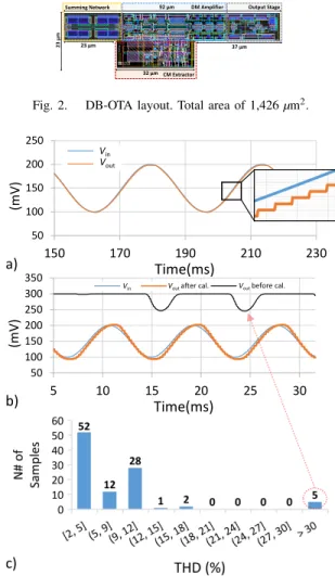
92 µm 23 µm 23 µm 32 µm 37 µm Summing Network DM Amplifier Output Stage
CM Extractor
Fig. 2. DB-OTA layout. Total area of 1,426µm2.
50 100 150 200 250 150 170 190 210 230 (m V) Time(ms) Vin Vout a) b) c) 50 100 150 200 250 300 350 5 10 15 20 25 30 (m V) Time(ms)
Vin Vout after cal. Vout before cal.
Vin Vout
Vin Voutafter cal. Voutbefore cal.
Fig. 3. a)VinandVoutforCout=80 pF,Vamp=50 mV andfin=30 Hz. b)Vin,
Voutbefore calibration (black) andVoutafter calibration (red) forCout=80 pF,
Vamp=50 mV and fin=120 Hz. c) 100 samples MC simulation for DB-OTA
THD (%).
inverters of theDM amplifier: thesumming network has been implemented using inverter-based pseudo-resistors as voltage dividers. Large area has been adopted in PMOS devices in Fig. 1 (a.1), to achieve a good matching leveraging Pelgrom’s law [12].
For what concerns the DM amplifier in Fig. 1 (a.2),
mis-match in the buffers VT decides the DB-OTA input offset
voltage and it has been mitigated by the calibration network in Fig. 1 (a.3). Such a calibration network includes four auxiliary pull-up (pull-down) branches, having pMOS (nMOS) devices with minimum length and binary weighted minimum width
(Wk=2kWmin,k=0. . .3) and driven by the same input signal,
which can be individually enabled/disabled depending on an 8-bit digital calibration word so that to modify the trip point of the buffer and effectively compensate mismatch. It is worth mentioning that this calibration network is also able to work in lowVDD.
III. SIMULATIONSRESULTS
The proposed DB-OTA has been laid out in 180nm CMOS so that to match the delays of the non-inverting and inverting
0 2,5 5 7,5 0 25 50 75 100
TH
D
(%)
Input V
amp(mV)
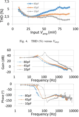
80pF 45pF 10pFFig. 4. THD (%) versusVamp
-20 0 20 40 60 1 10 100 1000 10000 Gain (dB)
Frequency (Hz)
80pF 45pF 10pF -200 -150 -100 -50 0 1 10 100 1000 10000 P h ase ( o)Frequency (Hz)
80pF 45pF 10pFFig. 5. ULV DB-OTA frequency response.
signal paths. The layout of the circuit, including the calibration network, occupies just 1,426µm2and it is shown in Fig. 2. The operation and performance of the DB-OTA have been tested by post-layout simulations performed in the voltage follower configuration and is then compared with ULV OTAs presented in recent literature.
A. Post-Layout Simulated Performance
The time-domain input and output waveforms of the
pro-posed DB-OTA atVDD=300mV, with sine wave input at 30Hz
frequency, 50mV peak amplitude andCout=80 pF capacitive
load are reported in Fig.3(a) and reveal the operation of the circuit as an opamp and less than 2% THD and 2nW power consumption. A zoom in the waveform shows the step-wise changes in vout resulting from digital operation. Fig. 4 depicts THD versusVampfor three differentCout=80,45,10 pF keeping fin=120 Hz.
1) Frequency Response: The frequency response of the circuit has been tested by time-domain, large-signal simula-tions, since small signal analysis cannot be adopted in view of the digital operation of the circuit. For this purpose, the DB-OTA has been tested in the voltage follower configura-tion with 50mV-peak-amplitude sine wave input at different frequencies f0, and the differential amplification frequency responseAd(f) =VVout(f)
d(f) has been estimated in magnitude and
phase taking the ratio of the Fast Fourier Transform (FFT)
at the fundamental frequency f0 of the output and of the
0.7nW 0.2nW 1.3nW Power Breakdown DM Amplifer: 35% CM Extractor: 10% Output Stage: 55%
Fig. 6. ULV DB-OTA Power Breakdown
709 780 1,020 840 551 246 31 10 11 12 13 10 100 1000 10000 200 250 300 350 400 450 500 [1 5 ] En e rg y (pJ ) FOM S (V -1) VDD (mV) FOM Energy[15] 0.2 0.6 2.0 7.9 23.2 126.0 7,000 0.10 0.23 0.85 2.37 4.06 9.… 54.00 0.01 0.10 1.00 10.00 100.00 1,000.00 0.1 1 10 100 1000 10000 200 250 300 350 400 450 500 Pow er ( nW ) VDD (mV) Power GBW G B W ( k H z)
Fig. 7. VDDversusFOMS, Power and GBW.
differential voltage. The DB-OTA frequency response reported in Fig.5 exhibit 35dB DC gain and 0.85,1.3 and 2.48 kHz Gain Bandwidth Product (GBW) with phase margin 76◦,68.5◦ and 57◦underCout=80,45 and 10 pF load, respectively.
2) Process Variations and Calibration: The uncalibrated
DB-OTA has been tested under process variations forVamp=
50 mV, Cout =80 pF and fin=120 Hz by Montecarlo (MC)
simulations performed on 100 samples and the output THD has been considered to evaluate the signal quality degradation. The histogram of the output THD reported in Fig.3(c) reveals a noticeable number of samples exceeding 10% THD due to the spread of the trip voltages of the DM amplifier ∆VT, which leads to high input offset voltage and results in the output saturation, as shown in Fig.3(b). From the same figure, however, the offset can be completely compensated by the proposed calibration network turning the DB-OTA back to work properly.
3) Power Consumption and Figure of Merit (FOM): For all
Coutvalues here explored the power consumption was found to be always lower than 2 nW. Fig. 6 shows the DB-OTA power breakdown forCout=80pF, at which it can be seen that 45% of the total power is used to process the input signal while the rest is used to chargeCout. The energy efficiency of the proposed
DB-OTA under low VDD has been also analyzed in Fig. 7
where the power, theGBWand the small signal figure of merit
FOMS=100GBW Cout(IDD)−1are plotted at differentVDD. It is interesting to note that there is a peak for FOMS around
VDD=300 mV, which coincides with the energy-efficientVDD optimum in digital sub- or near-threshold designs, regarding their most energy efficientVDD, i.e., their Minimum Energy
TABLE I
COMPARISONWITHSTATE-OF-THE-ARTULTRA-LOW-VOLTAGEOPERATIONALTRANSCONDUCTANCEAMPLIFIER
Performance [10]+ [6]+ [13]+ [14]+ [9]∗ [5]∗
MC-OTA
[5]∗
FFC-OTA This work
∗ Unit Technology 65 130 180 350 65 130 130 180 nm Supply Voltage 0.35 0.25 0.5 0.6 0.3 0.3 0.3 0.3 V DC Gain 43 60 52 69 60 46.2 49.8 35 dB GBW 3600 1.88 1,200 11.4 70 2,450 9,100 0.85 kHz Slew Rate 5600 0.7 2,890 14.6 25 2,400 3,800 0.5 V ms THD 0.6 0.2 1 0.08 - - - 3 % Phase Margin 56 52.5 - 65 53 52 76 76 o Cout 3 15 20 15 5 2 2 80 pF Power 17,000 18 110,000 550 51 1,800 1,800 2 nW Dia Area 5,000 83,000 26,000 60,000 3,000 - - 1,426 µm2 FOMS 19 29 0.11 0.18 2.05 81 303 1020 V−1 FOML 34.6 14.6 26.27 23.9 73.4 80 140 600 -+experimental;∗simulation;
Point (MEP). To illustrate, in Fig. 7 the notch filter MEP designed in [15] is also plotted. This result is expected since the DB-OTA processes the analog input information digitally.
B. Comparison with the State of the Art
Based on the post-layout simulation, compared to ULV OTAs proposed in recent literature, whose performance is summarized in Tab. I, the ULV DB-OTA presented here is
able to drive the highest Cout (x4 lager than [13]) at the
lowest power consumption (x9 lower than [6]) and shows itself as the most power-efficient topology for CMOS technology
consideringFOMSas a benchmark (x3.35 lager than [5]
FFC-OTA). The comparison in terms of both FOMS and FOML
is also illustrated in Fig. 8 including the performance of the proposed circuit samples after calibration and reveals that state-of-art performance is achieved even considering process variations. Moreover, the results of preliminary transistor-level simulations performed on the circuit ported to 40nm CMOS are also shown in Fig.8, demonstrating a further improved performance in finer technology, as expected for digital circuits and as not observed in traditional analog OTAs.
IV. CONCLUSION
By processing the analog input signal digitally with static logic gates, the ULV DB-OTA presented here has achieved
atVDD=300 mV aFOMS=1020 V−1consuming only 2 nW
and 1,426µm2of silicon area. The DB-OTA maximum
energy-efficient point has been demonstrated as well as its scalability. Through this implementation, this work moves forward against the common statement which states that, in general, analog integrated circuits do not take advantage of CMOS technology scaling.
REFERENCES
1 Alioto, M.,Enabling the Internet of Things – from Integrated Circuits to
Integrated Systems, 1st ed. Springer, 2017.
2 Pinckney, N., Blaauw, D., and Sylvester, D., “Low-Power Near-Threshold
Design: Techniques to Improve Energy Efficiency,” IEEE Solid-State
Circuits Magazine, vol. 7, no. 2, pp. 49–57, Spring 2015.
3 Dennard, R. H., “Past Progress and Future Challenges in LSI Technology:
From DRAM and Scaling to Ultra-Low-Power CMOS,”IEEE Solid-State
Circuits Magazine, vol. 7, no. 2, pp. 29–38, Spring 2015.
[10] [6] [13] [14] [9] [5] MC-OTA [5] FFC-OTA DB-OTA 40nm DB-OTA 180nm 5 50 500 5000 0.1 10 1000 100000 𝐹 𝑂 𝑀𝐿 = 100 𝑆𝑅 𝑎𝑣 𝑒 𝐶𝐿 𝐼𝐷𝐷 𝐹𝑂𝑀𝑆= 100 𝐺𝐵𝑊 𝐶𝐿 𝐼𝐷𝐷 (𝑉 −1)
Fig. 8. State-of-art plot for ULV OTA.
4 Crovetti, P. S., Musolino, F., Aiello, O., Toledo, P., and Rubino, R.,
“breaking the boundaries between analogue and digital,” Electronics
Letters, vol. 55, no. 12, pp. 672–673, 2019.
5 Lv, L., Zhou, X., Qiao, Z., and Li, Q., “Inverter-Based Subthreshold
Amplifier Techniques and Their Application in 0.3-V ∆Σ-Modulators,”
IEEE J. Solid-State Circuits, vol. 54, no. 5, pp. 1436–1445, May 2019. 6 Ferreira, L. H. C. and Sonkusale, S. R., “A 60-dB Gain OTA Operating
at 0.25-V Power Supply in 130-nm Digital CMOS Process,”IEEE Tran.
Circuits Syst. I: Reg. Papers, vol. 61, no. 6, pp. 1609–1617, June 2014. 7 Drost, B., Talegaonkar, M., and Hanumolu, P. K., “Analog Filter Design
Using Ring Oscillator Integrators,”IEEE J. of Solid-State Circuits, vol. 47,
no. 12, pp. 3120–3129, Dec 2012.
8 Lim, Y. and Flynn, M. P., “A 100 MS/s, 10.5 Bit, 2.46 mW
Comparator-Less Pipeline ADC Using Self-Biased Ring Amplifiers,”IEEE J. of
Solid-State Circuits, vol. 50, no. 10, pp. 2331–2341, Oct 2015.
9 Veldandi, H. and Shaik, R. A., “A 0.3-V Pseudo-Differential Bulk-Input
OTA for Low-Frequency Applications,” Circuits, Systems, and Signal
Processing, vol. 37, no. 12, pp. 5199–5221, Dec 2018.
10 Abdelfattah, O., Roberts, G. W., Shih, I., and Shih, Y., “An Ultra-Low-Voltage CMOS Process-Insensitive Self-Biased OTA with Rail-to-Rail
Input Range,”IEEE Tran. Circuits Syst. I: Reg. Papers, vol. 62, no. 10,
pp. 2380–2390, Oct 2015.
11 Crovetti, P. S., “A Digital-Based Analog Differential Circuit,”IEEE Trans.
Circuits Syst. I: Reg. Papers, vol. 60, no. 12, pp. 3107–3116, Dec 2013. 12 Galup-Montoro, C., Schneider, M. C., Klimach, H., and Arnaud, A., “A
Compact Model of MOSFET Mismatch for Circuit Design,”IEEE J. of
Solid-State Circuits, vol. 40, no. 8, pp. 1649–1657, Aug 2005. 13 Chatterjee, S., Tsividis, Y., and Kinget, P., “0.5-V Analog Circuit
Tech-niques and their application in OTA and filter design,”IEEE J. of
Solid-State Circuits, vol. 40, no. 12, pp. 2373–2387, Dec 2005.
14 Ferreira, L. H. C., Pimenta, T. C., and Moreno, R. L., “An Ultra-Low-Voltage Ultra-Low-Power CMOS Miller OTA With Rail-to-Rail
Input/Output Swing,”IEEE Trans. Circuits Syst. II: Exp. Briefs, vol. 54,
no. 10, pp. 843–847, Oct 2007.
15 Rosa, A. L. R., Soares, L. B., Stangherlin, K. H., and Bampi, S., “Designing CMOS for Near-Threshold Minimum-Energy Operation and
Extremely Wide V-F Scaling,” in 2015 28th Symposium on Integrated