Spin-Dependent Processes in Organic
Devices
Dissertation to obtain the academic degree
Dr. rer. nat.
submitted to the Departement of Physics of Freie Universität Berlin by:
Sebastian Schaefer
Betreuer: Dr. Wolfgang Harneit 1. Gutachter: Prof. Dr. R. Bittl
2. Gutachterin: Prof. Dr. M. Ch. Lux-Steiner Tag der Disputation: 2. Juni 2010
1
Abstract
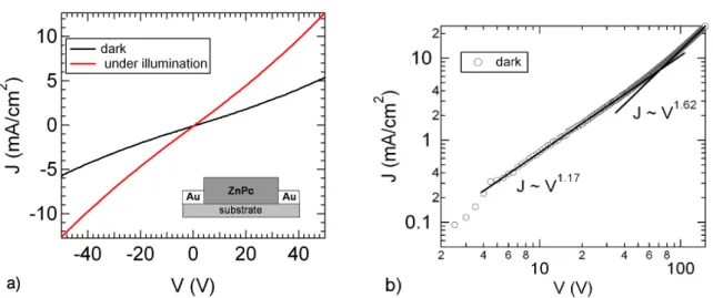
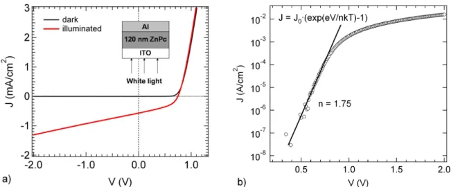
By bringing together a systematic IV-characterization and EDMR experiments, transport and degradation processes were studied in organic devices. In a first step, two Zinc phthalo-cyanine (ZnPc) single layer devices with different electrodes were investigated, a coplanar Au/ZnPc/Au sample and a sandwich type ITO/ZnPc/Al device. They served as a testbed for the correlation of IV- and EDMR measurements. The insights gained in this study were then applied to more complex bilayer ZnPc/C60-heterojunction solar cells.
A transport study at low voltages shows that bulk transport with Ohmic IV characteristics is dominant in the coplanar ZnPc, whereas the transport in the sandwich device is controled by a Schottky barrier at the aluminum contact. Both samples show SCL-currents with exponential trap distribution in the high voltage limit, characteristic for ZnPc. The degradation analysis indicate that the ITO/ZnPc/Al - device suffers from oxidation of the aluminum electrode, ex-hibiting a pronounced Schottky emission IV-behavior. This degradation could be prevented by an effective encapsulation, using a glass cover and UV-glue. The results of the solar cells also indicate an oxygen-induced degradation. This degradation is related to an increase of the resistivity in the C60layer, due to oxygen impurities.
The EDMR measurements indicate that polaron recombination is the dominant process in the organic devices investigated in this work. However the recombination process shows dis-tinct impact on the electric transport in the individual devices. Whereas the EDMR signal is photocurrent quenching in the coplanar sample it reverses sign in the sandwich device. The results of the transport measurements indicate a charge accumulation at the oxidized ZnPc/Al contact. As a consequence a model was proposed in which recombination involving these accumulated carriers can lead to a current enhancement. This model was verified by voltage dependent EDMR measurements, where it consistently explains a sign reversal when chang-ing from negative to positive bias.
In degraded solar cells a similar charge accumulation as in the ZnPc-layer is suspected. This charge accumulation manifests itself in an EDMR signal with identical properties to the one in ZnPc and is assumed to happen at the ZnPc/C60- interface, during degradation. Furthermore,
EDMR studies indicate that spin-dependent recombination happens during the exciton dis-sociation process at the ZnPc/C60 - interface, in the charged transfer complex (ZnPc+, C−
60).
This process is observed to quench the photocurrent in the solar cells.
In further spin studies Rabi beat oscillations under spin-locking conditions were observed for the first time in the EDMR of ZnPc and solar cells. This phenomenon exhibits a signal os-cillation at twice the Rabi-frequency that appears only when two pair spins are excited at the same time. The impact of this beat oscillation on EDMR lineshapes as well as its microwave power dependence were studied in detail. The effect of exchange coupling in the spin-pair was analyzed in the context of the beat oscillations and a lock in phase analysis.
Contents
1 Theoretical Background 11
1.1 Charge Transport in Organic Materials . . . 11
1.1.1 Space Charge Limited Currents (SCLC) . . . 12
1.1.2 SCLC in the Presence of Defect States . . . 13
1.2 Metal-Semiconductor Contacts . . . 14
1.2.1 Schottky Contact . . . 14
1.2.2 Fermi-Level Pinning . . . 16
1.3 Electron Spin Resonance (ESR) . . . 17
1.4 Electrically Detected Magnetic Resonance (EDMR) . . . 18
1.4.1 EDMR in Organic Semiconductor Devices . . . 19
1.4.2 Exchange Coupling in EDMR . . . 20
1.5 Pulsed Electrically Detected Magnetic Resonance . . . 22
1.5.1 Transient EDMR Signal . . . 22
1.5.2 Rabi Oscillation . . . 26 2 Experimental Background 33 2.1 Organic Materials . . . 33 2.1.1 Fullerene C60 . . . 33 2.1.2 Phthalocyanine . . . 36 2.2 EPR in ZnPc . . . 39
2.2.1 ZnPc Radical Cation g-Value determined by EPR . . . 39
2.3 Device Fabrication . . . 41
2.3.1 Coplanar Au/ZnPc/Au Samples . . . 42
2.3.2 Sandwich Devices for EDMR . . . 43
2.3.3 Sandwich Devices for IV-Characteristics . . . 44
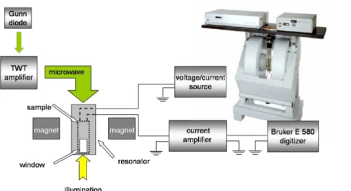
2.4 Experimental Setup . . . 45
2.4.1 IV-Glovebox-Setup . . . 45
2.4.2 EDMR Setup . . . 45 3
4 CONTENTS 3 Charge Transport in Phthalocyanine Devices 47
3.1 Bulk Transport in Au/ZnPc/Au Coplanar Devices . . . 47
3.1.1 IV-Temperature Dependency . . . 48
3.2 ITO/ZnPc/AL Schottky-Solar Cells . . . 50
3.2.1 IV-Characteristics (injection vs bulk properties) . . . 50
3.2.2 Degradation of the Al Contact Interface . . . 56
3.2.3 Encapsulation Revisited . . . 60
3.2.4 Discussion and Conclusions . . . 62
4 Spin Dependent Transport in ZnPc 65 4.1 Bulk Transport vs. Injection Limited Transport . . . 65
4.1.1 EDMR in Coplanar Au/ZnPc/Au Devices . . . 65
4.1.2 EDMR in ITO/ZnPc/Al Sandwich Devices . . . 67
4.2 EDMR Signal Saturation . . . 70
4.3 EDMR at Different Voltages . . . 70
4.4 The Role of Exchange Coupling in ZnPc . . . 72
4.4.1 Discussion of The Lineshapes . . . 73
4.4.2 Lock-In Phase Analysis . . . 75
4.5 Magnetoresistance in ZnPc . . . 78
5 Spin Dynamics in ZnPc 83 5.1 Pulsed EDMR in ZnPc Layers . . . 83
5.2 The Phenomenon of Spin-Locking . . . 86
5.2.1 Line Shapes Under Spin-Locking Conditions . . . 89
5.2.2 Beat Oscillations at different MW-Powers . . . 89
5.3 Pulsed EDMR in Au/ZnPc/Au Coplanar Devices . . . 90
5.3.1 Decoherence in Au/ZnPc/Au devices . . . 92
5.4 Discussion and Conclusions . . . 94
6 Spin-Dependent Transport in ZnPc/C60 Solar Cells 95 6.1 IV-Characteristics of Solar1new . . . 95
6.2 Spin Dependent Processes in Bilayer Cells . . . 98
6.2.1 Continuous Wave EDMR . . . 98
6.2.2 Discussion . . . 99
6.2.3 Pulsed EDMR in ZnPc/C60-Solar Cells . . . 100
6.2.4 Discussion . . . 101
6.3 Signal Decomposition by Light Intensity Control . . . 102
6.3.1 IV-Characteristic of Solar2new . . . 102
CONTENTS 5 6.3.3 EDMR Light Intensity Dependence . . . 106 6.4 Rabi Beat Oscillations . . . 108 6.5 Rabi Beat Oscillations of the Quenching Signal . . . 112
CONTENTS 7
Preface
In past years the potential of organic materials for optoelectronic devices and spintronic ap-plications has gained more and more attention. The extremely high absorption coefficients of some organic molecules facilitate the fabrication of low cost thin film photo-detectors and solar cells, whereas organic light emitting diodes (OLEDs) are already used in commercial displays and illuminants. Preparation methods of organic materials like spin coating and va-por jet printing pave the way for flexible devices like roll up displays.
Beside applications in conventional electronics, the observation of a giant magneto resistance (GMR) effect in organic spin valves [1] provides a route to organic spintronics. The underly-ing mechanism of the magnetoresistance effect in organic materials differs significantly from the classical picture and is a highly debated topic in current research. Although much efforts have been done in this field, the microscopic mechanisms in organic magnetoresistance as well as in magnetic resonance related methods (EDMR, ODMR, ELDMR, ...) are still un-clear. A better understanding of these microscopic processes would not only have impact on the field of spintronics and their applications, but could also help to identify current limiting processes and degradation mechanisms in conventional organic devices. Since the most seri-ous drawbacks in organic solar cells are still the low efficiency and the long term stability, the analysis of degradation and transport limitations is crucial for gaining a better device perfor-mance.
As a consequence, this work concentrates on the identification of transport limitations in or-ganic thin film devices by a continuous wave and pulsed EDMR study. The approach com-bines a fundamental current voltage study with a detailed EDMR analysis in zinc phthalo-cyanine (ZnPc) and ZnPc/C60-solar cells. The enhanced sensitivity of EDMR in comparison
to the conventional EPR makes this method an appropriate tool for the characterization of spin-dependent processes in thin film devices under realistic conditions such as white light illumination and room temperature. Since the limiting processes in organic samples are very complex, the study starts with simple one layer devices and progresses to more sophisticated bilayer solar cells. This approach offers the possibility to apply the results from the single layers ZnPc and from previous EDMR experiments on C60 [2, 3, 4] to the bilayer solar cell,
which facilitates the identification of the EDMR signals significantly.
Beside the influences of interfaces and electrode materials, also the effect of degradation on the device performance and the EDMR signal is examined. In the detailed pulsed EDMR analysis Rabi beat oscillations of non selectively excited spin pairs will be presented for the first time in EDMR of organics. This effect manifests itself in a signal oscillation at twice the Rabi frequency, when the two spins of a pair are excited at the same time. This phenomenon was previously observed in the reaction yield detected magnetic resonance (RYDMR) of rad-ical pairs. Furthermore the influence of exchange coupling will be investigated with the help
8 CONTENTS of a phase analysis in cw EDMR .
Chapter 1introduces the main transport mechanisms and semiconductor-metal-interface models which are needed in this work. This is followed by an overview of continuous wave and pulsed EDMR theory, which will be discussed in the frame of spin-dependent recombina-tion. The EDMR section contains also the influence of exchange coupling on the cw-spectrum and the consequences of selective and non selective excitation in pulsed experiments.
Chapter 2gives a short review about the electrical and optical properties of the organic materials ZnPc and C60. The results from previous EDMR measurements on C60 will be
dis-cussed and for ZnPc the g-value of the radical cation is determined by ESR measurements of iodine doped material which is helpful for the following EDMR study. Futhermore experi-mental details about device fabrication and measurement setups are given.
Chapter 3is a transport and degradation analysis on ZnPc single layer devices. The effect of different contact materials and geometries on the transport is studied in ZnPc thin film struc-tures. The results obtained on two representative device structures are discussed throughout the next chapters, a coplanar Au/ZnPc/Au device and an ITO/ZnPc/Al sandwich device. With the help of a current voltage analysis it can be shown which contacts provide bulk- or injection limited transport in ZnPc. The temperature and thickness dependence of the IV-measurements is used to characterize the influence of bulk transport and metal-semiconductor interfaces on the charge transport. Further experiments concentrate on degradation mechanisms in the sand-wich device and how this degradation can be prevented by an effective encapsulation.
Chapter 4presents continuous wave EDMR experiments on coplanar and sandwich type devices. Whereas the EDMR signal is first analyzed in the coplanar device, further stud-ies on the sandwich type ITO/ZnPc/Al sample treat the influence of the electrodes and the degradation on the EDMR signal. The spin-dependent processes is embedded in the transport model developed in chapter 3 to give a complete picture of the working device including loss mechanisms. This transport model is further supported by saturation and voltage dependent EDMR measurements, providing a more detailed view of the spin-dependent process. The influence of exchange coupling on the EDMR spectrum is discussed in the coplanar ZnPc device and analyzed with a lock-in phase analysis. The last section is concerned with mag-netoresitance observed in the coplanar ZnPc sample. The results were interpreted in terms of the spin-dependent recombination model used in the EDMR, bridging the gap between magnetoresistance and EDMR.
CONTENTS 9 Chapter 5treats the spin dynamics in the ZnPc single layer devices by means of a pulsed EDMR study. In the first section the pulsed EDMR spectrum is analyzed and compared to cw EDMR spectra. Beside this analysis, Rabi oscillations in the case of selective and non selec-tive excitation are discussed in the following sections and compared to theoretical predictions. This treatment includes the microwave power dependence of the Rabi beat oscillations and a lineshape analysis of pulsed EDMR spectra at pulse lengths shorter than the dephasing time. Furthermore the spin-dynamics are compared to the spin-locking phenomenon observed in radical pairs.
Chapter 6 presents results obtained on ZnPc/C60 bilayer solar cells. Including a brief
IV-characterization, the chapter begins with the analysis of the continuous wave and pulsed EDMR spectra at different voltages in the context of the previous measurements on the single layer ZnPc and C60 devices [2, 3, 4]. This part of the chapter deals with the identification of
the EDMR signals and discusses possible loss mechanisms and degradation in these devices. Further pulsed studies demonstrate how EDMR signals can be extracted by their distinct pho-tocurrent response on the light intensity. This is followed by a detailed analysis of spectrally resolved Rabi oscillations and a comparison between the spin dynamics of the signals.
Chapter 1
Theoretical Background
The following sections are intended to give the reader a short introduction into the theoretical framework of this work. The main transport mechanisms in organic semiconductors and the most important semiconductor-metal-interface models are presented in first sections. Since it provides the basics for the EDMR, the principles of Electron spin resonance (ESR) will be illustrated shortly afterwards. The following EDMR section treats the influence of exchange coupling on the spin level transitions and thus the cw-spectrum, whereas the last part of this chapter is concerned with the coherent spin motion in pulsed EDMR. This part explains how selective and non selective excitation influence the Rabi-oscillation of the spin pair ensemble.
1.1
Charge Transport in Organic Materials
Whereas charge transport pathways in inorganic semiconductors are provided by a bandstruc-ture due to strong exchange interactions of atomic orbitals in the crystal strucbandstruc-ture, organic solids are bound together by relatively weak Van der Waals - or π -π - interactions, which is rather inappropriate for electron transport. The weak bonding forces lead to intermolecular separations that are large compared to the separation of atoms and ions in inorganic crystal lattices. Consequently, the overlap of the molecular orbitals is rather weak, which leads to lower mobilities than in inorganic semiconductors. However, since many organic molecules consist of delocalized electrons, the intramolecular electron exchange can be still substantial, especially in aromatic ring structures. As a result, the mobility of an electron residing on an individual molecule is very large compared to the mobility of electrons that move from one molecule to another, while traversing the molecular crystal. Another consequence of the weak intermolecular forces is that the properties of a molecular crystal are primarily determined by the electronic properties of the molecules itself, which is in contrast to inorganic semiconduc-tors. The small overlap of the molecular orbitals inhibits the formation of extended energy bands. The energy band width depends on the spacing of the molecules, in which a large molecular spacing leads to narrow energy bands. If the energy band width is smaller or in the
12 CHAPTER 1. THEORETICAL BACKGROUND range of kBT, the molecular distances become too large for the electrons to tunnel from one
molecule to another. In this case charge transport is often described by a hopping process, where the electrons have to overcome the potential barrier ∆EJ between the molecules. The
hopping propability is [5]: WH=νJexp −∆EJ kBT (1.1) The attempt frequency νJ of the hopping depends on the exchange energy J, which can be
determined from EPR measurements. As condition for hopping transport, the carrier mobility should be smaller than µ ≈1cm2V−1s−1[5, 6]. However, since in many organic solids the mobilities are in the order ofµ≈1cm2V−1s−1it is difficult to decide a priori which transport model is appropriate. The low conductivities in organic materials can be overcome by doping, which was first demonstrated by Shikarawa et al. [7]. They showed that the conductivity of polyacetylene increased by several orders of magnitude upon doping by halogen (seven orders in the case of iodine doping). Furthermore extremely high absorption coefficients allow the production of very thin absorber layers in organic photodetectors and solar cells.
1.1.1
Space Charge Limited Currents (SCLC)
Space charge limited currents (SCLC) appear when the concentration of injected charge car-riers exceeds the concentration of thermally generated carcar-riers. Efficient carrier injection requires at least one ohmic contact to the organic layer, which provides a reservoir of charges. At low voltages, the concentration of injected carriers is rather low and the current is usually dominated by thermally generated carriers. This results in an Ohmic current density-voltage behavior:
J=p0eµV
d (1.2)
where p0 is the concentration of thermally generated holes (assuming a hole conductor), e
is the elementary charge and d is the spacing of the electrodes. When higher voltages are applied, in a way that the concentration of injected carriers becomes higher than the thermally generated ones, SCL currents will dominate the device. The organic layer is now treated as a perfect insulator between two electrodes, a situation similar to a parallel plate capacitor with chargeQgiven by:
Q=CV with C=ε0εr
A
d (1.3)
whereε0is the vacuum permittivity,εrthe dielectric constant of the organic layer and C is the
capacitance with plate area A and plate spacingd. Since in the case of carrier injection the charges do not reside on the plates, but distribute in the organic layer, the effective separation of the charge is not the plate distance d but a smaller value. The correct value of d will be included in the exact formula, calculated by Mark and Lampert [8]. If the injected space
1.1. CHARGE TRANSPORT IN ORGANIC MATERIALS 13 chargeQdrifts through the insulator with a transit timettransthis leads to a current density:
JSCLC∝
Q Attrans
(1.4) Inserting Eq.1.3 into Eq.1.4 leads to the following expression for the current density:
JSCLC∝
ε0εrV
dttrans
(1.5) The transit time is given byttrans=d/v, wherevis the speed of the carriers, which depends
on their drift mobilityµ and the external voltageV as: v=µV/d. Plugging the transit time ttrans=d2/µV into Eq.1.5 yields:
JSCLC ∝ε0εrµ
V2
d3 (1.6)
The exact formula for the space charge limited currents including the correct charge distribu-tion in the insulator is given by [8]:
JSCLC=
9 8ε0εrµ
V2
d3 (1.7)
The formula is called Child’s law and was derived for ideal trap free insulators.
1.1.2
SCLC in the Presence of Defect States
When traps are present in the organic layer only a part of the injected carriers may contribute to the current, whereas the other carriers are trapped. Consequently, Eq.1.7 has to be modified. However, the modification depends on the distribution of the trap states in the band gap. In several organic materials the traps exhibit an exponential distribution Nt(E)with respect to
the valence band edge:
Nt(E) =N0exp −kE BTC (1.8) where Nt(E) is the trap density per unit energy and unit volume, which decreases with the
distanceE from the valence band edge. N0 is the trap density at the valence band edge and
TC is a parameter that characterizes the width of the distribution (usually TC >T at room
temperature). If the traps in a sample show such a distribution, the current density can be expressed by a power law of the form:
JSCLC =eµNv εoεr eN0kBTC l Vl+1 d2l+1 (1.9)
14 CHAPTER 1. THEORETICAL BACKGROUND whereNvis the effective density of states in the valence band andlis a parameter that is given
by:
l= TC
T (1.10)
Figure 1.1: SCL current voltage characteris-tics of devices with exponential trap distribu-tion.
The IV-characteristics in a device with ex-ponential trap distribution is illustrated in Fig.1.1. At low voltages, where thermally generated carriers dominate the device cur-rent, an Ohmic IV-dependence is observed. As soon as the concentration of injected carriers exceeds that of thermally generated ones the current depends quadratically on the voltage. If the voltage is further in-creased, the Fermi-level shifts far into the trap band and the IV-characteristics become superquadratic. In the limiting case where all traps are filled, the IV-relation returns to the quadratic behavior until finally the current may saturate.
1.2
Metal-Semiconductor Contacts
1.2.1
Schottky Contact
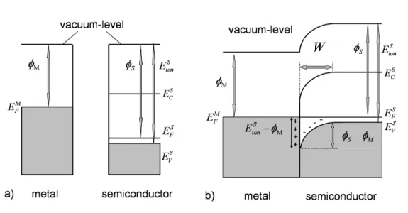
If a p- or n-type semiconductor is brought into contact with a metal, either an Ohmic or a rectifying contact is formed. Which of the two contacts is observed in an ideal metal-semiconductor junction depends on the workfunction of the metal and the metal-semiconductor. A rectifying contact is known as a Schottky barrier and arises when the workfunctionφS of
a p-type semiconductor is larger than the workfunction φM of the metal, see Fig.1.2 a). If
the materials are brought into contact, electrons flow from the metal into the semiconductor until the Fermi-levels of the metalEFM and the semiconductorEFS equalize each other. As the electrons move from the metal into the semiconductor, they recombine with free holes in the valence band of the semiconductor. As a result, the interface region of the semiconductor gets depleted of free holes leaving behind the negatively charged ionized acceptors. On the metal side, a thin layer of positive charges is formed within the Thomas-Fermi screening distance (≈ 0.5 Å) from the interface. The low concentration of free holes in the semiconductor leads to an increased distance between the Fermi levelEFS and the valence bandEVS near the interface. Since in thermal equilibrium the Fermi level remains constant throughout the semiconductor, the valence band edge bends down at the interface as shown in Fig.1.2 b). However, in the bulk of the semiconductor distant from the metal contact the Fermi level position does not
1.2. METAL-SEMICONDUCTOR CONTACTS 15
Figure 1.2: Formation of a Schottky barrier between a metal and a p-type semiconductor. a) before contact b) in contact.
change and the band diagram is the same as in Fig.1.2 a). The amount of bend-bending is given by the difference in the workfunctions of the metal and the semiconductor and is also known as the built in potential or the contact potential:
eVbi=φS−φM (1.11)
The contact potential has to be surpassed when holes enter the metal from the semiconductor side. On the other hand, when holes move from the metal into the semiconductor they have to surpass the Schottky barrier given by:
eVB=EionS −φM (1.12)
whereEionS is the ionization energy of the semiconductor, defined by the distance of the va-lence band edge to the vacuum energy. The shape of the barrier is determined by the acceptor distribution in the semiconductor. A uniform acceptor distribution gives rise to a parabolic barrier, known as the Schottky barrier, whereas the concentration of acceptors in the semicon-ductorNAcontrols the width of the depletion zone:
W =
r
2ε0εrVbi
eNA
(1.13) If a voltage is applied to the Schottky junction with the metal positively biased (reverse bias), hole injection from the metal into the semiconductor is hindered by the Schottky barrierVB.
The situation is illustrated in Fig.1.3 a) and shows that under these conditions the width of the depletion zone in the semiconductor increases. The resulting current flow is very weak. In
16 CHAPTER 1. THEORETICAL BACKGROUND
Figure 1.3: Schottky barrier under reverse a) and forward bias conditions b)
forward bias, the holes moving from the semiconductor into the metal have to surpass only the reduced contact potentialVbi−V . Fig.1.3 b) shows that the width of the depletion zone
de-creases in forward bias, which promotes current flow in this direction. Different mechanisms like tunneling and recombination can control the current across a Schottky barrier in forward bias. However the most important one is thermionic emission over the barrier, where only those holes that have an energy greater thane(Vbi−V)may surpass the barrier. The current
flow controlled by thermionic emission over the barrier is given by the Shockley equation:
J = J0 exp eV nkBT −1 (1.14) J0 = A∗T2exp −keVB BT (1.15) whereA∗=4πem∗kB2/his the effective Richardson constant,m∗is the effective mass andhis Planck’s constant. The diode quality factorndescribes the deviation from the ideal thermionic emission current and indicates that other transport mechanisms are present in the sample.
1.2.2
Fermi-Level Pinning
Practical experience shows that barriers at semiconductor-metal junctions often show weaker dependence on the metal workfunctionφM than predicted by the Schottky theory. This weak
correlation between the barrier height and the metal workfunction may arise when localized surface states are present in the semiconductor. These surface states can stem from imperfec-tions at the surface of the crystal structure, especially in covalently bounded semiconductors, were dangling bond give rise to defect levels in the band gap. However Fermi-level pinning was suggested also for C60 fullerene -layers [9]. After a model of Bardeen [10] the surface
1.3. ELECTRON SPIN RESONANCE (ESR) 17
Figure 1.4: Fermi-level pinning scheme.
states are distributed continuously in the bandgap and have neutral levelφ0, see Fig.1.4. All
surface levels below φ0 are occupied and act like donor levels, which means that they are
neutral when occupied but positive when empty. The surface levels above the neutral level are acceptor like and become negative when they are occupied. In order to reach equilibrium, electrons move from the semiconductor into the surface states until the Fermi-level at the sur-face and in the bulk material are aligned. The result is a positively charged depletion zone in the semiconductor and a negatively charged surface. The band bending leads to the forma-tion of a surface barrier even without contact to a metal. If the semiconductor is brought into contact with a metal, carriers are exchanged between the metal and the surface states without strongly effecting the barrier. In this case the Fermi level is said to be pinned.
1.3
Electron Spin Resonance (ESR)
Transitions between electronic states with different quantum numbers ms can be detected by
electron spin resonance. Since the quantum number ms determines the orientation of the
electron spin with respect to an external magnetic field B0, a change in ms is equivalent to a
change in the direction of the spin. In order to describe the interaction of the spin with the external magnetic field it is necessary to introduce the magnetic moment of the electron spin:
µs=
p
s(s+1)µBg (1.16)
wheresis the spin quantum number,µBis the Bohr magneton and g is the Landé factor. In the presence of a magnetic field B0the component of the magnetic moment parallel (antiparallel)
18 CHAPTER 1. THEORETICAL BACKGROUND to this field is given by:
µsz =∓
1
2gµB (1.17)
Since the potential energy of the magnetic moment in the external field isE =−−→µ ·−→B the transition energy between the corresponding sublevels is:
∆E=gµBB0 (1.18)
If the paramagnetic sample is exposed to radiation with a frequencyν, transitions between the spin sublevels may be induced if the condition:
hν=gµBB0 (1.19)
is fulfilled. In ESR the absorption of radiation by the sample is detected. Experimental prac-tice shows that in most cases it is convenient to use a constant microwave frequency and measure the absorption as a function of the magnetic field B0.
1.4
Electrically Detected Magnetic Resonance (EDMR)
Introduction
Electron spin resonance (ESR) is a well known method to characterize charge carriers, de-fects and impurities in solids. This has been demonstrated for example in amorphous silicon (a-Si:H) where the silicon dangling bond defect was identified by means of ESR [11, 12]. However, the sensitivity of conventional ESR is limited to a number of ∼ 1011 spins per Gauss line width [13], which is too low to investigate for example interfaces in thin film devices. An appropriate experimental method for detailed studies of microscopic transport and loss mechanisms should be able to identify transport processes with a sensitivity many orders of magnitude higher than ESR. This can be achieved by replacing the conventional detection of the microwave absorption by an electrical detection setup. As a result, not only the sensitivity is enhanced but also the object of investigation changes. In an EDMR ex-periment the conductivity of a device changes, while sweeping the magnetic field through resonance in the presence of microwave irradiation. The reason for the conductivity changes are spin-dependent processes like recombination, hopping or tunneling. This is in contrast to ESR which is not sensitive to processes but to paramagnetic species. Consequently EDMR is able to identify microscopic transport mechanisms as long as they depend on spin selec-tion rules. Most of the early models describing the conductivity changes under ESR rely on spin-dependent recombination mechanism investigated in silicon devices [14, 15, 16, 17, 18]. Basically the recombination of two charge carriers depends on their relative spin orientation
1.4. ELECTRICALLY DETECTED MAGNETIC RESONANCE (EDMR) 19 and is only permitted when the spins point in opposite directions, also called singlet configura-tion (S = 0). This follows from the conservaconfigura-tion of the angular momentum, if the ground state of the recombining pair is also assumed to be a singlet state. Magnetic resonance increases the number of singlet spin pairs in the sample and therefore leads to an enhancement of the recom-bination rate. The early theory of spin-dependent recomrecom-bination, introduced by D. J. Lépine [14] is based on the polarization of the spin ensemble. In this model free carriers recombine at recombination centers. The spin lattice relaxation is assumed to be faster than the recombi-nation and in thermal equilibrium there will be an enhanced population of triplet states due to the polarization. Applying electron paramagnetic resonance to the sample tends to equalize the population of all spin sublevels which leads to a ratio of 1/4 : 3/4 for singlet to triplet states. Since the polarization is rather weak at room temperature p≈gµBB0/kBT ≈10−3the
expected EDMR signal strength is also very weak ∆σ/σ ≈ p2≈10−6. This is in contrast to various experimental results, that show larger EDMR signals [19, 20, 21], and therefore cannot hold for those systems. The Kaplan-Solomon-Mott (KSM) model [15] is based on the assumption that localized electrons and holes form an intermediate pair state with consider-able lifetime before they dissociate or recombine spin-dependently. In contrast to the model of Lépine it requires the recombination to be faster than the spin lattice relaxation. As a result the system cannot get into thermal equilibrium and a high amount of pairs with triplet spin con-figuration will accumulate in the sample. Since this model is not based on the weak thermal polarization at room temperature, higher signal strength are predicted that are in agreement with the experimental results. Further investigations in silicon based semiconductors revealed various other spin-dependent mechanisms, such as hopping and tunneling, summarized in a survey of M. Stutzmann et. al [13].
1.4.1
EDMR in Organic Semiconductor Devices
Reports about EDMR measurements with continuous microwave irradiation can be found for small molecules [20, 21, 22, 23, 24] as well as for polymer devices [24, 25, 26, 27]. The most frequently used models to explain the EDMR signals in organic materials are spin-dependent polaron recombination and bipolaron formation. Bipolarons are assumed to be spinless parti-cles (S = 0) that consist of two like charged polarons. The binding energy of the bipolarons is assumed to stem from the polarization of the lattice [28]. If the attractive interaction of the two polarons with the polarized dielectric medium exceeds the repulsive coulomb interaction this may lead to a bound bipolaron. Furthermore, the formation of bipolarons is possible only when the precursor polarons have a singlet spin configuration and is therefore spin-dependent. As far as polaron pair recombination is concerned, we want to follow the polaron reencounter model, introduced by T. Eickelkamp et al. [21]. This model derives from the radical pair recombination model and considers different g-factors for the negative and positive polarons
20 CHAPTER 1. THEORETICAL BACKGROUND as well as spin-spin-interactions within the pair. After light excitation excitons are generated in organic semiconductor that dissociate into free polarons. These polarons may reencounter in the organic semiconductor and form non geminate polaron pairs with random spin config-uration. As in the KSM model it is assumes that the polarons form a long living intermediate pair state prior to the recombination process. In general the outcome of recombination and bipolaron formation is a current quenching, but for different reasons. The result of enhanced recombination under magnetic resonance is the annihilation of an electron and a hole. Since both carriers can in principle contribute to the current if the spin pair dissociates, the elimi-nation of them leads to a reduction of charge carrier concentration and the current decreases. The enhanced formation of bipolarons in magnetic resonance is also assumed to decrease the current since bipolarons are less mobile carriers than polarons. However under specific cir-cumstances both mechanisms may lead also to a current enhancement, this will be discussed in the experimental section.
1.4.2
Exchange Coupling in EDMR
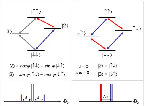
In the absence of spin-spin-coupling an EDMR-spectrum is assumed to comprise the two spectral features of the precursor spin pair. However, exchange coupling within the pair leads to four energy level with four allowed transitions. The effect of the exchange coupling to the spectral lines becomes apparent from the Spin-Hamiltonian containing the Zeeman interaction of both spins and an expression for the exchange interaction between them:
ˆ H ¯ h = ˆ HZ+HˆJ ¯ h =ωaSaz+ωbSbz−JSa·Sb (1.20) whereωa,bare the Larmor frequencies of spins a and b of the pair,Saz,bzare the z-components
of the spinoperatorsSa,band J is the exchange coupling constant. In this analysis, the dipolar coupling within the spin pair and hyperfine interactions are neglected. The spin eigenstates in the pure Zeeman basis according to ˆHZ can be denoted as: |↑↑i,|↑↓i,|↓↑i,|↓↓iin the product
space of the spins a and b: |↑↑i=|↑ia⊗ |↑ib. The corresponding energy level are given by: E1Z = h¯ 2(ωa+ωb) E2Z = h¯ 2(ωa−ωb) E3Z = −h¯ 2(ωa−ωb) E4Z = −h¯ 2(ωa+ωb) (1.21)
and the transitions are simply the Larmor frequencies of the two spins, see also Fig.1.5 b). However, in the Zeeman basis the Hamiltonian in Eq.1.20 is not diagonal and thus the spin
1.4. ELECTRICALLY DETECTED MAGNETIC RESONANCE (EDMR) 21 basis has to be transformed to diagonalize the Hamiltonian. The transformed spin basis reads:
|1i = |↑↑i
|2i = cosϕ|↑↓i −sinϕ|↓↑i
|3i = sinϕ|↑↓i+cosϕ|↓↑i
|4i = |↓↓i (1.22)
with tan(2ϕ) =J/δ ω andδ ω =ωa−ωb. The states|2iand|3iare mixed states with singlet
content, where recombination is partially allowed, whereas the pure triplet level|1iand|4i, also denoted by|T+iand|T−irespectively, inhibit recombination. In the case of strong
cou-plingJ≫δ ω (ϕ =π/4 ) eigenstate|2ibecomes a pure singlet state |Si= √1
2(|↑↓i − |↓↑i),
whereas eigenstate|3ibecomes a triplet state|T0i= √12(|↑↓i+|↓↑i). The energy levels
ac-cording to the new spin states are now a function of the exchange coupling constant: E1 = h¯(ω0−J 4) E2 = h¯(J4+Ω2J) E3 = h¯(J4− ΩJ 2 ) E4 = h¯(−ω0−J4) (1.23) where ω0 = (ωa+ωb)/2, and ΩJ = √
δ ω2+J2. As a result of the shifted energy levels the partial degeneracy of the four transition lines is lifted and the corresponding transitions between these four spin states are given by:
∆E1−2 = E1−E2=h¯(ω0−J 2− ΩJ 2 ) ∆E1−3 = E1−E3=h¯(ω0−J2+Ω2J) ∆E2−4 = E2−E4=h¯(ω0+J2+Ω2J) ∆E3−4 = E3−E4=h¯(ω0+J 2− ΩJ 2 ) (1.24)
In general four lines will appear in the spectrum. However, if the coupling constant J be-comes significantly larger than the Larmor separation δ ω, the transitions ∆E1−3 and∆E3−4
(indicated by the grey arrows in the level scheme of Fig.1.5 a)) tend towards each other. For J≫δ ω andΩJ ≈Jthe transitions become one center line and two satellites separated by J:
22 CHAPTER 1. THEORETICAL BACKGROUND
Figure 1.5: Energy level and spin-states in the exchange coupled spin pair (left) and without exchange coupling (right) with the correlated stick spectra indicated below.
The transition probability of the center lines increase relative to the satellites with increasing J, which becomes apparent from the expression for the transition strengthω1jk=|hj|H1/h¯|ki|:
ω1(12) = ω1(24)=ω1p1−sin2ϕ
ω1(13) = ω1(34)=ω1p1+sin2ϕ (1.26)
where H1/h¯ =ω1(Sxa+Sxb) is the microwave Hamiltonian in the rotating frame in angular
frequency units. In Fig.1.5 the energy levels and transitions (arrows) of the spin pair are illustrated in the case of exchange coupling a) and without b). The resulting spectral features are shown in the stick spectrum below. In general, strong exchange coupling leads the triplet system |T+i,|T0i,|T−i to decouple from the singlet state |Si. As aresult the transition rate
between the triplet and the singlet system is very weak, resulting in a weak or even absent EDMR signal. The effect of exchange coupling on the EDMR spectrum will be discussed in § 4.4.
1.5
Pulsed Electrically Detected Magnetic Resonance
1.5.1
Transient EDMR Signal
The theoretical treatment of pulsed EDMR will be discussed in the framework of spin-dependent recombination, as proposed by C. Boehme and K. Lips [29, 30]. The recombination mech-anism assumed by Boehme and Lips includes trapped electrons in a deep lying level center
1.5. PULSED ELECTRICALLY DETECTED MAGNETIC RESONANCE 23 in the bandgap of a semiconductor, whereas this work will focus on spin-dependent recom-bination of oppositely charged polaron pairs as assumed in the polaron reencounter model, introduced by T. Eickelkamp [21]. As mentioned in the previous sections the recombination raterdepends on the spin configuration of the spin pair and is assumed to be much higher for a singlet state, than for a triplet configuration (rS≫rT ). In general the spin pair is in one of
the the four spin states given in Eq.1.22. Whereas states|1iand|4iare pure triplet states that decay withrT , the recombination rate of the mixed spin states|2iand|3ican be determined
by taking into account the singlet and triplet content of the states:
ri=rS|hi|Si|2+rT|hi|T0i|2, i=2,3 (1.27)
where the singlet and the triplet states have been defined previously as √1
2(|↑↓i ∓ |↓↑i). The
recombination ratesr1−4 can be evaluated by plugging the four eigenstates into Eq.1.28 and
using the definitiontan(2ϕ) =J/δ ω, which yields:
r1,4 = rT r2 = r2S 1+ J ΩJ +rT 2 1− J ΩJ r3 = r2S 1− J ΩJ +rT 2 1+ J ΩJ (1.28) After a pulsed resonant microwave excitation the spin pair ensemble will show a change in the recombination rate with respect to the situation before excitation. This is a result of the change in spin state occupation, due to the microwave induced transitions. In the following the spin state occupation of the pair ensemble is expressed in the density matrix formalism [31], where the diagonal matrix elementsρii= pi|iihi|represent the occupation density in the spin states
|ii. This is equivalent to the probabilitypito find the ensemble in the state|ii. The occupation
differences between the diagonal elements characterize the polarization of the ensemble. The off diagonal elementsρi j of the the density matrix represent the coherence on the transition
between state |iiand |ji. Applying a pulsed microwave excitation of pulse length τ to the spin ensemble changes the density matrix entries. As a result the total recombination rate is altered which leads to a change in the density of the electrons∆ne(t,τ)and holes∆nh(t,τ)in
the sample. The conductivity change , given by:
∆σ(t,τ) =e(∆ne(t,τ)µe+∆nh(t,τ)µh) (1.29)
whereµeandµhare the mobilities of the electrons and the holes respectively. If the mobilities
of the charge carriers are assumed to be constant the conductivity change originates only from the variation of the electron and hole densities which are influenced by the decay and gen-eration of the precursor spin pairs. Under constant illumination the spin pairs are generated
24 CHAPTER 1. THEORETICAL BACKGROUND
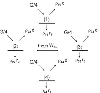
Figure 1.6: Generation, dissociation, recombination and relaxation rates within the spin pair ensemble in an EDMR experiment.
by light excitation and it can be assumed that all four spin levels are populated uniformly by the generation rate G/4, as illustrated in Fig.1.6. However, the spin level will be depopulated by recombination and dissociation rates. Since the polaron pairs are localized carriers, the only way they can contribute to the current is by dissociation into free polarons. If we as-sume a common dissociation rated for all spin level the charge carrier density change can be expressed by: ∆ne(t,τ) =∆nh(t,τ) =τLd 4
∑
i=1 (ρˆii(t,τ)−ρˆii(τ)) (1.30)where ˆρii(t,τ) are the diagonal density matrix elements at timet after the state at the end of
the microwave pulse ˆρii(τ)andτLis the lifetime of the carriers. For simplicityτL is assumed
the same for electrons and holes. The term ˆρii(t,τ)−ρˆii(τ) represents the transient density
matrix changes in the spin pair ensemble due to recombination and dissociation after the pulsed excitation of lengthτ. Since the coherent density changes during the microwave pulse are much faster than the recombination processes, they will be discussed separately in the following section. Plugging Eq.1.30 into Eq.1.29 yields an expression for the conductivity change:
∆σ(t,τ) =eτL(µe+µh)d
∑
i=1,...,4(ρˆii(t,τ)−ρˆii(τ)) (1.31)
Since the time dependency of ∆σ(t,τ) has its origin in the population changes of the den-sity matrix elements, the time dependency of (ρˆii(t,τ)−ρˆii(τ))has to be expressed in a rate
model. This rate model manifests itself in a set of differential equations, according to the rate picture given in Fig.1.6. Each of the four spin pair level will be populated by 14 of the generation rate G and depopulated by the appropriate dissociation and recombination rates,
1.5. PULSED ELECTRICALLY DETECTED MAGNETIC RESONANCE 25 leading to the following expression:
˙ ρ11 ˙ ρ22 ˙ ρ33 ˙ ρ44 = −d−rT 0 0 0 0 −d−r2 0 0 0 0 −d−r3 0 0 0 0 −d−rT ρ11 ρ22 ρ33 ρ44 +G 4 1 1 1 1 (1.32)
where the intersystem crossing rate WISC is neglected here for simplicity. The equilibrium
solutions ˙ρii=0 of this equation yield:
ρ11eq,44 = G 4(d+rT)
ρ22eq,33 = G 4(d+r2,3)
(1.33) The general solutions of the homogeneous part of Eq.1.32 are exponential functions of the form:
ρ11,44(t,τ) = Tr{ρˆeq}∆11,44(τ)e−(d+rT)t
ρ22,33(t,τ) = Tr{ρˆeq}∆22,33(τ)e−(d+r2,3)t (1.34)
where the amplitudes∆ii(τ)are the microwave induced density changes during a pulsed exci-tation of lengthτ. These density changes read:
∆11,44(τ) = ρ11,44(τ)−ρ eq 11,44 Tr{ρˆeq} ∆22,33(τ) = ρ22,33(τ)−ρ eq 22,33 Tr{ρˆeq} (1.35) with
∑
i=1,...,4 ∆ii(τ) =0 sinceTrρˆ =TrρˆeqIn general the recombination ratesr2andr3 are much stronger than the triplet recombination
raterT and the dissociation rated. This leads to an overpopulation of the triplet level in the
steady state prior to the microwave pulse, which can be expressed by:
ˆ ρeq≃ G 4(d+rT) 0 0 0 0 0 0 0 0 0 0 0 0 0 0 G 4(d+rT) (1.36)
As a result the density changes in Eq.1.35 are negative for the triplet states which are de-populated during microwave excitation and positive for the mixed states with singlet
con-26 CHAPTER 1. THEORETICAL BACKGROUND tent, since their population increases. The density changes are normalized by the trace of
ˆ
ρeq: Tr{ρˆeq}=G/2(d+r
T). With these results the general expression for the conductivity
changes given in Eq.1.31 can be rewritten in the form:
∆σ(t,τ) =eτL(µe+µh)dG 2(d+rT) h ∆22(τ)e−(d+r2)t+∆ 33(τ)e−(d+r3)t+ (∆11(τ) +∆44(τ))e−(d+rT)t i (1.37) In principle ∆σ(t,τ) is a multi exponential decay with positive components for the singlet states and a negative component for the triplets. The large singlet recombination ratesr2,3≫
rT lead to very fast decay of the positive signal components. In the case where the response
time of the setup or the sample is longer than 1/r2,3, the positive contributions cannot be
observed, which is also discussed in the work of Hiromitsu et al [32]. If exchange coupling is weak Eq.1.28 shows that the recombination rates becomer2=r3= (rS+rT)/2, and Eq.1.35
and 1.37 simplify. In this case the equation for the conductivity change becomes:
∆σ(t,τ) = eτL(µe+µh)dG 2(d+rT)
(∆11(τ) +∆44(τ))he−(rS−2rT)t−1
i
e−(d+rT)t (1.38)
Although this expression contains only three parameters (rS,rT,d) that determine the transient
rise and decay of the signal, in real devices impedances from the electrical setup and the device will be superimposed on the signal. Consequently, the determination of the rate constants is a rather difficult task.
1.5.2
Rabi Oscillation
The previous section treated the impact of the density changes ˆρii(t,τ)−ρˆii(t,τ)after a pulsed
microwave excitation on the conductivity of the sample. The density changes result from generation-, recombination- and dissociation rates, that control the population of the spin states of the spin pair ensemble. However, these rates are assumed to have time constants much longer than the microwave pulse length, and therefore play a minor role during the pulsed excitation. The density changes during the pulse ∆ii(τ) are the result of microwave induced transitions between the spin states and reflect the coherent spin nutations of the spin ensemble. The following analysis neglects any incoherent processes as relaxational processes and spin-spin interactions during the microwave pulse. This simplification can be made, be-cause in general the spin-spin interaction is weak with respect to the Zeeman interaction and since high microwave powers are used in the pulsed measurements, the spin-spin interaction is also weak compared to the microwave field. The spin relaxation times were found to be rather long (10−7-10−3 s) [33, 34, 35] in organic materials due to the weak spin-orbit
cou-pling and therefore can be neglected during the very short (10−7s) microwave pulses. The
1.5. PULSED ELECTRICALLY DETECTED MAGNETIC RESONANCE 27 where the pulsed microwave excitation is treated as a time dependent external perturbation.
Figure 1.7: Illustration of the spin motion un-der the influence of a static magnetic field B0
and an oscillating microwave magnetic field B1. In the rotating frame the oscillating field B1becomes fixed and the static field is
compen-sated when the resonance condition is fulfilled. The spin precesses around the vector~nawhich
becomes parallel to B1at resonance.
In a constant magnetic field B0 the spin ~Sa precesses aound the axis parallel to B0
with the Larmor frequencyωa=gaµBB0/h¯.
When the microwave is turned on during an EPR or EDMR experiment, the microwave magnetic fieldB1in the resonator has a
com-ponent that precesses aroundB0with the
fre-quencyωmwin the same direction as the spin.
If the microwave frequencyωmwmatches the
Larmor frequency exactly the spin will be fixed relative toB1in the rotating frame, this
situation is illustrated in Fig.1.7. In the ro-tating frame the static magnetic field B0 is
compensated and the spin starts to precess around the remaining fieldB1, inducing
tran-sitions between the spin up and down states.
However, when the resonance condition is not exactly fulfilled, B0 is not fully compensated
and the spin will precess around a effective field that points along the vector~na, given by: ~na=
ωmw−ωa
Ωa −→ez +
γB1
Ωa−→ex (1.39)
where Ωa=p(γB1) + (ωmw−ωa) is the Rabi frequency of spin~Sa. The precession of the
spin around the axis~naduring the microwave excitation of pulse lengthτcan be expressed by
the operator: ˆ Dan(Ωaτ) =exp −h¯i~Sa·~naΩaτ =11cos 1 2Ωaτ −i~σ·~nasin 1 2Ωaτ (1.40) where~σ= (σx,σy,σz)are the Pauli matrices and 11 is the unit matrix. This operator represents
represents the spin oscillation in the rotating frame. For a complete description of the spin motion the transformation into the rotating frame has to be included by :
ˆ
Danz(Ωa,ωmw,τ) =Dˆz(ωmwτ)Dˆan(Ωaτ)Dˆz(ωmwτ) (1.41)
Since EDMR is always concerned with a pair of spins~Saand~Sbthe operator ˆDanz(Ωa,ωmw,τ)
has to be expressed in the product space of the the two spins, which yields: ˆ
28 CHAPTER 1. THEORETICAL BACKGROUND where ˆDbnz(Ωb,ωmw,τ) is the operator associated with the precession of spin~Sb around the
axis~nb. Since the operator ˆDpair(Ωa,Ωb,ωmwτ) describes the spin precession of both spins
during the microwave pulse, the evolution of spin pair ensemble starting from the steady state density matrix given in Eq.1.36 is given by:
ˆ
ρ(τ) =Dˆpair(Ωa,Ωb,ωmwτ)ρˆeqDˆ†pair(Ωa,Ωb,ωmwτ) (1.43)
The results for ˆρ(τ) can be plugged directly in Eq.1.35 for the microwave induced density changes which yield for the triplet state densities:
∆11,44(τ) = ρ11,44(τ)−ρ eq 11,44 Tr{ρˆeq} = " cos2 1 2Ωaτ + ωmw−ωa Ωa 2 sin2 1 2Ωaτ # × " cos2 1 2Ωbτ + ωmw−ωb Ωb 2 sin2 1 2Ωbτ # +sin2 1 2Ωaτ sin2 1 2Ωbτ γB1 Ωa 2 γB1 Ωb 2 −1 (1.44)
This formula is a general expression for the density changes of the triplet states and is rather lengthy but it can by simplified by taking into account a few assumptions concerning selective and not selective excitations. The density changes of the mixed states have a similar time dependence as the triplet states and can be found in [30].
Selective Excitation (
δ ω
≫
γ
B
1)
If the Larmor frequenciesωa,bof spin~Saand~Sbare well separated, the spins can be addressed
individually by the microwave field. In the case were the microwave field is resonant with spin
~Sa, spin~Sbwill be far off resonantωmw−ωb≫γB1. This situation allows selective excitation
of both spins and is observed when the condition for large Larmor separation (δ ω ≫γB1) is
fulfilled. This case makes the following approximations reasonable: ωmw−ωb
Ωb ≈1,
γB1
Ωb ≈0 (1.45)
With these assumptions Eq.1.44 simplifies to:
∆11,44(τ) =−γ 2B2 1 Ω2a sin 21 2Ωaτ =−1 2 γ2B21 Ω2a [1−cos(Ωaτ)] (1.46)
which reflects the Rabi-oscillations of the resonant spin~Sawith the frequencyΩawhereas spin
~Sb is offresonant at the same time. The situation is totally symmetric when spin~Sbbecomes
1.5. PULSED ELECTRICALLY DETECTED MAGNETIC RESONANCE 29 general two resonance lines according to the two spins of the pair are expected in the EDMR spectrum.
Non Selective Excitation (
δ ω
≪
γ
B
1)
If the Larmor frequenciesωa,b of spin~Saand~Sbare very close, both spins will be excited at
the same time by the microwave field, which makes a selective excitation of the individual spins impossible. As a result the Larmor frequencies ωa,b of the individual spins can be
expressed by the average Larmor frequency of the spin pairω0= (ωa+ωb)/2 . This leads to
the following approximations: ωmw−ωa Ωa 2 ≈ ωmw−ωb Ωb 2 ≈ ωmw−ω0 Ω0 2 (1.47) and Ωa≈Ωb≈Ω0= q γ2B21+ (ωmw−ω0) (1.48)
As a result Eq.1.44 simplifies to the following expression:
∆11,44(τ) =−1 2 γ2B21 Ω20 sin 2(Ω 0τ)−12γ 2B2 1(ωmw−ω0)2 Ω40 sin 41 2Ω0τ (1.49) where the second term becomes zero under resonance conditions ωmw−ω0. Neglecting the
second term yields for the density changes:
∆11,44(τ) =−1 2 γ2B21 Ω20 sin 2 (Ω0τ) =−1 4 γ2B21 Ω20 [1−cos(2Ω0τ)] (1.50)
This result states that in the case of small Larmor separation (δ ω ≪γB1) the state density
oscillates with twice the Rabi-frequency 2Ω0. This phenomenon will be investigated in § 5.2,
where it is compared to the spin locking effect in reaction yield detected magnetic resonance in radical pairs. In general spin ~Sa and~Sb often exhibit Larmor distributions that have an
overlap region were the doubled Rabi frequency observed. This is frequently accompanied by spin pairs that have large Larmor separation and show only the regular Rabi-frequency.
The Function T(
α
)
The solutions gained for selective and non selective excitation in Eq.1.46 and 1.50 do not include Larmor distribution of the spins~Sa and~Sb of the pair. Since such distributions are
often observed in radical pairs [36, 37], they should be added for a complete description. This can be achieved by introducing functions of the Larmor frequencies Φ(ωa) and Φ(ωb) for
30 CHAPTER 1. THEORETICAL BACKGROUND whole spin pair ensemble can be expressed by the integral:
∆e f f(τ) = ˆ ∞ −∞ ˆ ∞ −∞ Φ(ωa)Φ(ωb)∆11,44(τ)dωadωb (1.51)
Considering the two cases of selective and nonselective excitation once more, the two integrals in Eq.1.51 can be simplified to a single one. During selective Excitation only one of the spins has to be considered, whereas the other one is off resonant. In the case of non selective excitation a common Larmor distribution Φ(ω0) for both spins can be assumed. A general
equation for the effective density changes can be given by:
∆e f f(τ,ωmw) = ˆ +∞ −∞ φ(ωL) 1 2κ γ2B21 (γB1)2+ (ωmw−ωL)2 sin2 κ q (γB1)2+ (ωmw−ωL)2τ dωL (1.52) whereωL andκ are parameters that depend on the type of excitation
1. Selective excitation: (δ ω ≫γB1): =⇒ ωL=ωa and κ=
1 2 2. Non selective excitation: (δ ω ≪γB1): =⇒ ωL=ω0 and κ=1(1.53)
Eq.1.52 reflects the coherent Rabi-oscillation of a spin pair ensemble during the microwave pulse for the cases of selective or non selective excitation. Although Larmor distributions are included, the formula describes only the extreme cases of complete selective or complete non selective excitation. Since in general only a part of the spin pair ensemble is non selectively
Figure 1.8: The transient function T(α) reflects the Rabi oscillation of the spin ensemble during the microwave pulse. The turning angle α =Ωτ depends on the pulse length. The data for T(α)were obtained from numerical integration.
excited, the complete ensemble has to be described by a superposition of different density functions∆e f f(τ,ωmw), as demonstrated in § 6.4. Eq.1.52 can be simplified when the Larmor
1.5. PULSED ELECTRICALLY DETECTED MAGNETIC RESONANCE 31 time dependence of∆e f f(τ,ωmw)is of interest. In this case Eq.1.52 can be simplified to:
T(α) = ˆ +∞
−∞
sin2α√1+x2
1+x2 dx (1.54)
where α =κγB1τ is the turning angle and x= (ωmw−ωL)/γB1. It can be shown that the
transient function T(α) is related to the Bessel function of the first kind J0:
T(α) =π ˆ α
0 J0(2x)dx (1.55)
Neither Eq.1.52 norT(α)can be integrated analytically, which makes fitting procedures rather complicated. However, it is possible to fit the derivative of the data by the integrand ofT(α) or∆e f f(τ,ωmw)and carry out a numerical integration afterwards. The result of an numerical
Chapter 2
Experimental Background
This chapter provides informations about the organic materials and their preparation as well as the experimental foundations used in this work. It begins with the electrical and optical properties of the organic materials ZnPc and C60. Whereas the section on fullerenes also
reviews the results from previous EDMR measurements on C60 the part concerning the
ph-thalocyanines contains a discussion about the the g-values of the ZnPc radicals. Since it will be useful for the interpretation of the EDMR spectra the ZnPc radical cation g-factor will be determined by ESR measurements of iodine doped material. The last part of this chapter contains information about the device fabrication and the experimental setup.
2.1
Organic Materials
2.1.1
Fullerene C
60The Fullerenes were discovered experimentally in 1985 by H. W. Kroto, J. R. Heath, S. C. O´Brian, R. F. Curl, and R. E. Smalley during experiments on carbon clusters [38]. However, the existence of C60was already predicted by Eiji Osawa in 1970 [39] in a Japanese magazine.
The structure of C60 containing 12 pentagons and 20 hexagons of carbon atoms arranged in
an Ih-symmetry is spherical and resembles a football. Besides diamond, graphite and coal,
the fullerenes are a new form of carbon, with outstanding properties. The spherical symmetry makes the molecule very stable and enables thermal deposition from the vapor phase. In solid bulk material fullerenes are bound by weak Van der Waals interaction showing an fcc-structure. Thin films are often polycrystalline with grain sizes dependent on the substrate temperature during vacuum evaporation. At room temperature the grains are approximately 50 nm in diameter [4] with increasing grain size for higher substrate temperatures. A review of the electronic and conductive properties are given in [40, 41].
34 CHAPTER 2. EXPERIMENTAL BACKGROUND Conductivity and electronic structure
Fullerene thin films are n-type semiconductors with a room temperature conductivity ranging between σ =10−8Ω−1cm−1 [40] andσ =10−6Ω−1cm−1 [42]. The semiconducting prop-erties are a result of the electronic energy level in C60 which show a gap between the fully
occupied HOMO and the LUMO of approximately EGap= 2.3 eV, see Fig.2.1 a). This value
was determined by Lof et al. [43] using photo electron spectroscopy (PES) and inverse PES. Additional optical excitations at 1.6eV and 1.8 eV were attributed to Frenkel type excitons with singlet and triplet character, respectively. C60 thin films are assumed to have a band
structure similar to disordered semiconductors with band tail states and deep levels in the band gap. The width of the electronic bands is about 0.4 eV.
Figure 2.1: a) C60 bandgap, b) absorption spectrum of C60-thin film, taken from[44]
Sensitivity to Gases
C60 thin films are extremely sensitive to oxygen exposure. The conductivity decreases by
many orders of magnitude under oxygen atmosphere to values down to σ =10−14Ω−1cm−1 [41, 42]. It is assumed that oxygen induces impurity states in the bandgap which can act as trapping or recombination centers. Other gases like nitrogen or argon have no effect on the conductivity of C60.
Mobility
The majority charge carriers in C60 are electrons with a mobility ofµe=1cm 2
V s [45], whereas
mobility of the holes is much smallerµh=10−4cm 2
V s . The conduction mechanism at moderate
temperatures can be described by hopping via band tail states and changes only at very high temperatures (near sublimation temp.) to band transport [41].
2.1. ORGANIC MATERIALS 35 Photoconductivity and Optical Absorption
The absorption spectrum of a C60thin film is shown in Fig.2.1 b). The direct HOMO- LUMO
transition (hu⇒t1u, 2.3 eV,λ≈540 nm) is optically forbidden and therefore the strong
absorp-tion peaks are due to higher excitaabsorp-tions. In general, illuminaabsorp-tion of C60 leads to generation
of excitons that can dissociate in the bulk or at interfaces, which leads to free charge carriers (polarons). The spectral photoconductance follows roughly the absorption spectrum, how-ever most features are rather due to excitonic than interband transitions. Upon illumination, C60also shows some special properties like photopolymerization and persistent
photoconduc-tivity. The former is the spontaneous formation of dimers and oligomers upon illumination with UV- or white light. The polymerization was found to have rather weak influence on the electronic levels of C60 [40] and is reversible upon heating over 100°C. Persistant
pho-toconductivity is a phenomenon where the dark current is increased after illumination of the sample. The increased dark conductivity can persist for seconds, hours or days, until the primary conductivity is reached again.
EDMR in C60
Continuous wave EDMR measurements in C60 have been reported by Brandt [19],
Eick-elkamp [21] and Hiromitsu [46]. All authors found a photocurrent quenching signal at g-values in the range of g = 2.0017 - 2.0020 with similar linewidth (0.3 - 0.65 mT). While the details of the spectral features of these EDMR signals differ considerably, the origin of the signals was consistently interpreted as spin-dependent recombination of oppositely charged carriers. Brandt and Eickelkamp used a model where photogenerated non-geminate positive and negative polarons form an exchange coupled pair, before they recombine spin depen-dently. In contrast to that Hiromitsu assumes an electron hole recombination at impurity centers in the C60 material. This is supported by the observation of spin-flip satellites from impurity protons in his sample.
Furthermore, ESR measurements of C60 layers also show an impurity signal [47], with a
similar linewidth and g-factor (g = 2.0023, ∆B = 0.25 mT) as the EDMR signal, and was
previously assigned to different forms of negative C60 radicals [48, 49]. These impurities are
also discussed in photo luminescence detected magnetic resonance (PLDMR) [50, 51] and light induced magnetic resonance (LESR) [52] of C60 films. Reed and Bolskar [53] assume
C120or C120O impurities as a possible origin of the ESR signal. Pulsed EDMR measurements,
which we carried out in a previous work [2, 3], show that the major feature of the EDMR res-onance is a narrow spin 1/2 peak consistent with the impurity signal mentioned by Reed and Bolskar. Additional Raman measurements could also reveal pronounced polymerization of the C60 sample [3], which supports the presence of C120 species. However, a final proof for
36 CHAPTER 2. EXPERIMENTAL BACKGROUND
2.1.2
Phthalocyanine
Phthalocyanine is a synthetic blue dye that was mentioned for the first time by A. Braun and J. Tcherniac [54] in 1907, when they worked with phthalamide. Nowadays it is used as pigment for plastics and paints, or as photoconducting material in laser printers. A review of the structure and electrical conduction properties of phthalocyanine thin films was given by R. D. Gould [6].
Morphology
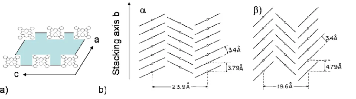
The chemical formula of metalfree phthalocyanine H2Pc is shown in Fig.2.2 a). The central
ring of this planar organic molecule consists of a system of 18 delocalized π-electrons and bears resemblance to the porphyrins [55]. In metal-phthalocyanines, such as ZnPc (Fig.2.2
Figure 2.2:a) metal free phthalocyanine structure, b) zinc phthalocyanine (ZnPc) structure
b), the two central hydrogen atoms are replaced by a single metal atom. With a diameter of
∅=1.5nm[56] ZnPc is small and stable enough to be thermally evaporated. J. M.
Robert-son [57], who investigated metalfree, nickel, copper and platinum phthalocyanines with X-ray reflection techniques pointed out, that the crystal structures of the parent phthalocyanine and many of the metallic derivatives are dimensionally very similar, therefore the following struc-tural properties are assumed to apply also for ZnPc. The phthalocyanine solid exhibits a monoclinic lattice structure (a6=b6=c,α =γ =90°,β ≥90°) with two molecules per unit cell, where the molecules are stacked in columns in the b-dimension. Fig.2.3 b) shows two kinds of arrangements of CuPc molecules, theα and theβ phase of the crystal lattice. The in plane distance of the molecules is the same for both modifications, but the inclination changes. Physical vapor deposited CuPc films were investigated by M. Ashida et al [58]. Sublimation at room temperature on a muscovite substrate yields polycrystalline material inα-phase with small fractions of the β-phase. Heating the sample up to T = 300° generates more and more β-phase fractions. It was also found by H. Peisert et al [59] that on a rough surface like indium tin oxide (ITO) the inclination is much higher due to less interaction of the molecules with the
2.1. ORGANIC MATERIALS 37
Figure 2.3:a) lattice structure dimensions a and c, b) stacking angle of CuPc in lattice direc-tion b. taken from [58]
substrate, therefore the phthalocyanine molecules are rather standing on the ITO-surface. This has also influence on the conductivity of phthalocyanine thin films, since theπ-orbital overlap is much stronger along the stacking axis b, the conductivity is higher in this direction, this was analyzed by J. M. Assour [60]. It also becomes plausible from this argument that the conductivity must be lower forβ-phthalocyanines, since the stacking distance b is larger, as confirmed by Kanemitsu et al for H2Pc [61]
Conductivity
The values for the Conductivity ofα-ZnPc given in the literature ranges betweenσ = 10−7Ω−1cm−1
[5] andσ = 10−8-10−13Ω−1cm−1[62].
Figure 2.4:a) ZnPc bandgap, b) absorption spectrum of phthalocyanine, taken from [44]
Electronic Structure
The ionization energyEion=5.28eVand the electron affinityeχ=3.34eV of ZnPc evaporated
thin films were determined by W. Gao and A. Kahn [63] using UPS and IPES techniques. The resulting direct bandgap between HOMO and LUMO is 1.94eV with these values, as illustrated in Fig.2.4 a). They state that the Fermi-level position is near midgap in the undoped


![Figure 3.7: a) Proposed energy level diagram for the ITO/ZnPc/Al Schottky barrier cell, the HOMO and LUMO energy is taken from Gao and Kahn [63], the lower limit for the ZnPc Fermi level is related to the open circuit voltage determined from the IV-charact](https://thumb-us.123doks.com/thumbv2/123dok_us/1300621.2674192/57.892.142.765.578.824/figure-proposed-diagram-schottky-barrier-related-circuit-determined.webp)