EET1240/ET212
EET1240/ET212
Electronics
Electronics
Semiconductors and Diodes
Semiconductors and Diodes
Electrical and Telecommunications
Engineering Technology Department
Professor Jang
Prepared by textbook based on “Electronics Devices” by Floyd, Prentice Hall, 7thedition.
Outline
Outline
• Semiconductor Physics
• The PN junction
• Biasing the PN junction
• The diode
• Trouble Shooting
ET212 Electronics – Semiconductors Floyd 2
Key Words: Semiconductor, Silicon, PN Junction, Forward Bias, Reverse Bias, Diode
Introduction
Introduction
Forward bias Current flows Reverse Bias No current flowThe basic function of a diode is to restrict current flow to one direction.
ET212 Electronics – Semiconductors Floyd 3
Bohr model of an atom
Bohr model of an atom
As seen in thismodel, electrons circle the nucleus. Atomic structure of a material
determines it’s ability to conduct or insulate.
FIGURE 1 The Bohr model of an atom showing electrons in orbits and around the nucleus, which consists of protons and neutrons. The “tails” on the electrons indicate motion.
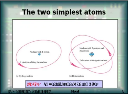
The two simplest atoms
The two simplest atoms
FIGURE 2 The two simplest atoms, hydrogen and helium.
ET212 Electronics – Semiconductors Floyd 5
Conductors, Insulators, and Semiconductors
Conductors, Insulators, and Semiconductors
¾
The ability of a material to conduct current is
based on its atomic structure.
¾
The orbit paths of the electrons surrounding the
nucleus are called shells.
¾
The less complete a shell is filled to capacity the
more conductive the material is.
¾
Each shell has a defined number of electrons it
will hold. This is a fact of nature and can be
determined by the formula, N
e= 2n
2.
¾
The outer shell is called the valence shell.
ET212 Electronics – Semiconductors Floyd 6
• All elements are arranged in the periodic table of the
elements in order according to their
atomic number
.
The atomic number equals the number of protons in the
nucleus, which is the same as the number electrons.
• Electron shells
and
Orbits
• The outmost shell is known as the Valence shell and
electrons in this shell are called
valence electrons
.
• The process of losing a valence electron is known as
ionization
(i.e.
positive ion
and
negative ion
).
Atomic number
Atomic number
,
,
Electron shells & Orbits
Electron shells & Orbits
,
,
Valence electrons, and Ionization
Valence electrons, and Ionization
ET212 Electronics – Semiconductors Floyd 7
Electron shells and Orbits
Electron shells and Orbits
FIGURE 3 Energy levels increase as the distance from the nucleus increases.
Conductors, Insulators,
Conductors, Insulators,
and Semiconductors
and Semiconductors
• A
conductor
is a material that easily conducts
electrical current. The best conductors are
single-element material, such as copper, gold, and aluminum,
which are characterized by atoms with only one valence
electron very loosely bound to the atom.
• An
insulator
is a material that does not conduct
electrical current under normal conditions. Valence
electrons are tightly bound to the atoms.
• A
semiconductor
is a material that is between
conductors and insulators in its ability to conduct
electrical current. The most common single –element
semiconductors are silicon, germanium, and carbon.
ET212 Electronics – Semiconductors Floyd 9
Energy Bands
Energy Bands
FIGURE 4Energy band diagram for a pure (intrinsic) silicon crystal with unexcited atoms. There are no electrons in the conduction band.
ET212 Electronics – Semiconductors Floyd 10
The valence shell determines the ability of material to conduct current.
A Copper atom has only 1 electron
in it’s valence ring. This makes it a
good conductor. It takes 2n
2electrons or in this case 32
electrons to fill the valence shell.
A Silicon atom has 4 electrons in
its valence ring. This makes it a
semiconductor. It takes 2n
2electrons or in this case or 18
electrons to fill the valence shell.
Conductors, Insulators, and Semiconductors
Conductors, Insulators, and Semiconductors
FIGURE 5
Diagrams of the silicon and copper atoms.
ET212 Electronics – Semiconductors Floyd 11
Covalent Bonding
Covalent Bonding
Covalent bonding is a bonding of two or more atoms by the interaction of their valence electrons.
FIGURE 6
Silicon and Germanium
Silicon and Germanium
FIGURE 7 Diagrams of the silicon and germanium atoms.
ET212 Electronics – Semiconductors Floyd 13
Conduction in Semiconductors
Conduction in Semiconductors
FIGURE 9Energy band diagram for a pure (intrinsic) silicon crystal with unexcited atoms. There are no electrons in the conduction band.
ET212 Electronics – Semiconductors Floyd 14
N
N
-
-
type and P
type and P
-
-
type Semiconductors
type Semiconductors
The process of creating N and P type materials is called doping.
Other atoms with 5 electrons
(pentavalent atom) such as
Antimony are added to Silicon
to increase the free electrons.
N-type
Other atoms with 3 electrons
(trivalent atoms) such as Boron are
added to Silicon to create a deficiency
of electrons or hole charges.
P-type
ET212 Electronics – Semiconductors Floyd 15
The Depletion Region
The Depletion Region
With the formation of the p and n materials combination of electrons and holes at the junction takes place.
p region n region
p region n region
This creates the depletion region and has a barrier potential. This potential cannot be measured with a voltmeter but it will cause a small voltage drop.
Biasing the Diode :
Biasing the Diode :
Forward and Reverse Bias
Forward and Reverse Bias
Voltage source or bias connections are + to the p material and – to the n material
Bias must be greater than .3 V for Germanium or .7 V for Silicon diodes. The depletion region narrows.
Voltage source or bias connections are – to the p material and + to the n material. Bias must be less than the break down voltage.
Current flow is negligible in most cases. The depletion region widens.
Forward Bias
Reverse Bias
ET212 Electronics – Semiconductors Floyd 17
Forward Bias
Forward Bias
FIGURE 10 A forward-biased diode showing the flow of majority carriers and the voltage due to the barrier potential across the depletion region.
ET212 Electronics – Semiconductors Floyd 18
Reverse Bias
Reverse Bias
FIGURE 11 The diode during the short transition time immediately after reverse-bias voltage is applied.
ET212 Electronics – Semiconductors Floyd 19
Forward Bias Measurements With
Forward Bias Measurements With
Small
Small
Voltage Applied
Voltage Applied
In this case with the voltage applied is less than the barrier potential so the diode for all practical purposes is still in a non-conducting state. Current is very small.
Forward Bias Measurements With Applied
Forward Bias Measurements With Applied
Voltage
Voltage
Greater Than the Barrier Voltage
Greater Than the Barrier Voltage
.
.
With the applied voltage exceeding the barrier potential the now fully forward biased diode conducts. Note that the only practical loss is the .7 Volts dropped across the diode.
ET212 Electronics – Semiconductors Floyd 21
Ideal Diode Characteristic Curve
Ideal Diode Characteristic Curve
In this characteristic curve we do not consider the voltage drop or the resistive properties. Current flow proportionally increases with voltage.
ET212 Electronics – Semiconductors Floyd 22
V
V
-
-
I Characteristic for
I Characteristic for
Forward Bias
Forward Bias
(a) V-I characteristic curve for forward bias. Part (b) illustrates how the dynamic resistance r’ddecreases as you move up the curve (r’d= ∆VF/∆IF).
ET212 Electronics – Semiconductors Floyd 23
V
V
-
-
I Characteristic for
I Characteristic for
Reverse Bias
Reverse Bias
V-I characteristic curve for reverse-biased diode.
The complete
The complete
V
V
-
-
I characteristic curve
I characteristic curve
for a diode
for a diode
ET212 Electronics – Semiconductors Floyd 25
Forward-bias and reverse-bias connections
showing the diode symbol.
ET212 Electronics – Semiconductors Floyd 26
Practical Diode Characteristic Curve
Practical Diode Characteristic Curve
In most cases weconsider only the forward bias voltage drop of a diode. Once this voltage is overcome the current increases proportionally with voltage.This drop is particularly important to consider in low voltage applications.
ET212 Electronics – Semiconductors Floyd 27
The Ideal Diode Model
The Ideal Diode Model
V
F= 0 V
LIMIT BIAS FR
V
I
=
I
R= 0 A
V
R= V
BIASThe Practical Diode Model
The Practical Diode Model
V
F= 0.7 V (silicon)
V
F= 0.3 V (germanium)
LIMIT F LIMIT R R F BIASR
I
V
V
V
V
LIMIT=
=
−
−
0
LIMIT F BIAS FR
V
V
I
=
−
ET212 Electronics – Semiconductors Floyd 29
The Complete Diode Model
The Complete Diode Model
'
7
.
0
F
d
F
I
r
V
=
+
'7
.
0
d LIMIT BIAS Fr
R
V
I
+
−
=
ET212 Electronics – Semiconductors Floyd 30
Troubleshooting Diodes
Troubleshooting Diodes
Testing a diode is quite simple, particularly if the multimeter used has a diode check function. With the diode check function a specific known voltage is applied from the meter across the diode.
K A A K
With the diode check function a good diode will show
approximately .7 V or .3 V when forward biased.
When checking in reverse bias the full applied testing voltage will be seen on the display.
ET212 Electronics – Semiconductors Floyd 31
Troubleshooting Diodes
Troubleshooting Diodes
Open Diode
In the case of an open diodeno current flows in either direction which is indicated by the full checking voltage with the diode check function or high resistance using an ohmmeter in both forward and reverse connections.
Shorted Diode
In the case of a shorted diodemaximum
current flows indicated by a 0 V with the diode check function or low resistance with an ohmmeter in both forward and reverse connections.
Diode Applications
EET1240/ET212
Electronics
Electrical and Telecommunications
Engineering Technology Department
Professor Jang
Prepared by textbook based on “Electronics Devices” by Floyd, Prentice Hall, 7thedition.
Outlines
¾
Half Wave Rectifiers
¾
¾
Full Wave Rectifier
Full Wave Rectifier
¾
¾
DC Power Supply Filter and Regulator
DC Power Supply Filter and Regulator
¾
¾
IC Regulator
IC Regulator
¾
¾
Zener
Zener
Diode
Diode
¾
¾
Troubleshoot
Troubleshoot
ET212 Electronics – Diodes and Applications Floyd 2
Key Words: Half Wave, Full Wave, Rectifier, Power Supply, Regulator, Zener
Introduction
The basic function of a DC power supply is to convert an AC voltage (110 V, 60 Hz) to a smooth DC voltage.
The rectifiercan be either a half- or Full-wave rectifier. The rectifier convert the ac input voltage to a pulsating dc voltage.
The filtereliminates the fluctuation
in the rectified voltage and produces a relatively smooth dc voltage.
The regulatoris a circuit that maintains a constant dc voltage for variations in the input power line voltage or in the load.
ET212 Electronics – Diodes and Applications Floyd 3
Half Wave Rectifier
A half wave rectifier(ideal) allows conduction for only 180°or half of a complete cycle. The output frequency is the same as the input. The average VDC or VAVG= Vp/π
When the sinusoidal input voltage (Vin)
goes positive, the diode is forward-biased and conducts current through the load resistor. The current produces an output voltage across the load RL.
When the input voltage goes negative during the second half of its cycle, the diode reversed-biased. There is no current, so the voltage across the load resistor is 0 V.
The net result is that only the positive half-cycles of the ac input voltage appear across the load. Since the output does not change polarity, it is pulsating dc voltage with a frequency of 60 Hz.
Average value of the half-wave rectified signal
θ θ π π θ π d V area V V v p AVG p∫
= = = 0 sin 2 1 2 sin π π π π π p p p p V V V V = = − − − − = − − − = ) 2 ( 2 )] 1 ( ) 1 ( [ 2 )] 0 cos ( cos [ 2ET212 Electronics – Diodes and Applications Floyd 5
Ex 2-1
What is the average value of the half-wave
rectified voltage in Figure?
V
V
V
AVG p31
.
8
100
=
=
=
π
π
ET212 Electronics – Diodes and Applications Floyd 6
Effect of the Barrier Potential on the
Half-Wave Rectified Output
The effect of the barrier potential on the half-wave rectified output voltage is to reduce the peak value of the input by about 0.7 V.
ET212 Electronics – Diodes and Applications Floyd 7
Ex 2-2
Sketch the output voltages of each rectifier for the indicated input voltage, as shown in Figure. The IN4001 and IN4003 are specific rectifier diodes.The peak output voltage for circuit (a) is Vp(out)= Vp(in)– 0.7 V
= 5 V – 0.7 V = 4.30 V The peak output voltage for circuit (b) is
Vp(out)= Vp(in)– 0.7 V
= 100 V – 0.7 V = 99.30 V
Half Wave Rectifier - Peak Inverse Voltage (PIV)
Peak inverse voltage is the maximum voltage across the diode when it is in reverse bias. The diode must be capable of withstanding this amount
of voltage. PIV = Vp(in)
The PIV occurs at the peak of each half-cycle of the input voltage when the diode is reverse-biased. In this circuit, the PIV occurs at the peak of each negative half-cycle.
ET212 Electronics – Diodes and Applications Floyd 9
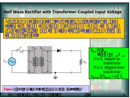
Half Wave Rectifier with Transformer-Coupled Input Voltage
FigureHalf-wave rectifier with transformer-coupled input voltage.
Transformer coupling provides two advantages. First, it allows the source voltage to be stepped up or stepped down as needed. Second, the ac source is electrically isolated from the rectifier, thus preventing a shock hazard in the secondary circuit.
Vsec= nVpri
where n = Nsec/Npri
If n>1, stepped up transformer If n<1, Stepped down
transformer
Vp(out)= Vp(sec)– 0.7 V
ET212 Electronics – Diodes and Applications Floyd 10
Ex 2-3
Determine the peak value of the output voltage
for Figure if the turns ratio is 0.5.
Vp(pri)= Vp(in)= 156 V
The peak secondary voltage is Vp(sec)= nVp(pri) = 78 V
The rectified peak output voltage is Vp(out)= Vp(sec)– 0.7 V
= 78 V – 0.7 V = 77.3 V
ET212 Electronics – Diodes and Applications Floyd 11
Full-Wave Rectifiers
π
p AVGV
V
=
2
A full-wave rectifier allows current to flow during both the positive and negative half cycles or the full 360º. Note that the output frequency is twice the input frequency.
Ex 2-4
Find the average value of the full-wave rectified
voltage in Figure.
V
V
V
AVG=
2
p=
2
(
15
)
=
9
.
55
π
π
ET212 Electronics – Diodes and Applications Floyd 13
The Center-Tapped Full-Wave Rectifier
This method of rectification employs two diodes connected to a center-tapped transformer. The peak output is only half of the transformer’s peak secondary voltage.
ET212 Electronics – Diodes and Applications Floyd 14
ET212 Electronics – Diode Applications Prof. Jang 15
Full-Wave Center Tapped
Note the current flow direction during both alternations. Being that it is center tapped, the peak output is about half of the secondary windings total voltage. Each diode is subjected to a PIV of the full secondary winding output minus one diode voltage drop
PIV = 2Vp(out)+ 0.7V
Center-tapped
full-wave rectifier with a
transformer turns
ratio of 2.
Center-tapped
full-wave rectifier with a
transformer turns
ratio of 1. V
p(pri)is
the peak value of the
primary voltage.
Full Wave Rectifier - Peak Inverse Voltage (PIV)
) 2 ( ) 7 . 0 2 (Vp(sec) Vp(sec) PIV = − − − V V V V V p p p 7 . 0 7 . 0 2 2 (sec) (sec) (sec) − = − + = Vp(out)= Vp(sec)/2 – 0.7 V Vp(sec)= 2Vp(out)+ 1.4 V PIV = 2Vp(out)+ 0.7 VThe peak inverse voltage across D2is
Ex 2-5
Show the voltage waveforms across each half of the secondary winding and across RLwhen a 100 V peak sine wave is applied to the primarywinding in Figure. Also, what minimum PIV rating must the diodes have?
Vp(sec)= nVp(pri)= 0.5(100 V) = 50 V
There is a 25 V peak across each half of the secondary with respect to ground. The output load voltage has a peak value of 25 V, less the 0.7 V drop across the diode.
PIV = Vp(sec)– 0.7 V = 50 V – 0.7 V = 49.3 V
ET212 Electronics – Diodes and Applications Floyd 18
The Full-Wave Bridge Rectifier
The full-wave bridge rectifier takes advantage of the full output of the secondary winding. It employs four diodes arranged such that current flows in the direction through the load during each half of the cycle.When the input cycle is positive as in part (a), diode D1and D2are forward-biased and
conduct current in the direction shown. A voltage is developed across RLwhich looks
like the positive half of the input cycle. During this time, diodes D3and D4are
reverse-biased.
When the input cycle is negative as in part (b), diode D3and D4are forward-biased and
conduct current in the same direction through RLas during the positive half-cycle. During
negative half-cycle, D1and D2are
reverse-biased. A full-wave rectified output voltage appears across RLas a result of this action.
ET212 Electronics – Diodes and Applications Floyd 19
The Full-Wave Bridge Rectifier-Peak Inverse Voltage
Bridge Output Voltage: Vp(out)= Vp(sec) Vp(out)= Vp(sec)- 1.4 V
The Full-Wave Bridge Rectifier
The PIV for a bridge rectifier is approximately half the PIV for a center-tapped rectifier.PIV=Vp(out)+0.7V
Note that in most cases we take the diode drop into account.
ET212 Electronics – Diodes and Applications Floyd 21
Ex 2-6
Determine the peak output voltage for the bridge rectifier in Figure. Assuming the practical model, what PIV rating is required for the diodes? The transformer is specified to have a 12 Vrmssecondary voltage for thestandard 110 V across the primary.
Vp(sec)= 1.414Vrms= 1.414(12 V) ≈17 V
Vp(out)= Vp(sec)- 1.4 V = 17 V – 1.4 V = 15.6 V
PIV = Vp(out) + 0.7 V = 15.6 V + 0.7 V = 16.3 V
ET212 Electronics – Diodes and Applications Floyd 22
Power Supply Filters And Regulators
As we have seen, the output of a rectifier is a pulsating DC. With filtration and regulation this pulsating voltage can be smoothed out and kept to a steady value.Figure illustrates the filtering concept showing a nearly smooth dc output voltage from filter. The small amount of fluctuation in the filter output voltage is called
ripple.
ET212 Electronics – Diodes and Applications Floyd 23
Power Supply Filters and Regulators
A capacitor-input
filter will charge and
discharge such that it
fills in the “gaps”
between each peak.
This reduces
variations of voltage.
This voltage variation
is called ripple
voltage.
Power Supply Filters And Regulators
The advantage of a full-wave rectifier over a half-wave is quite clear. The capacitor can more effectively reduce the ripple when the time between peaks is shorter.ET212 Electronics – Diodes and Applications 25
Ripple Factor
Ripple Factor
The ripple factor (r)is an indication of the effectiveness of the filter and defined as
r = Vr(pp) / VDC ) ( ) ( ) ( ) 2 1 1 ( ) 1 ( rect p L DC rect p L pp r V C fR V V C fR V − ≅ ≅
ET212 Electronics – Diodes and Applications Floyd 26
ET212 Electronics – Diode Applications Prof. Jang 27
Surge Current in the Capacitor-Input Filter
Being that the capacitor appears as a short during the initial charging, the current through the diodes can momentarily be quite high. To reduce risk of damaging the diodes, a surge current limiting resistor is placed in series with the filter and load.IC Regulators
IC Regulators
Power Supply Filters And Regulators
Regulation is the last step in eliminating the remaining ripple and maintaining the output voltage to a specific value. Typically this regulation is performed by an integrated circuit regulator. There are many different types used based on the voltage and current requirements.ET212 Electronics – Diodes and Applications Floyd 29
Power Supply Filters and Regulators
How well the regulation is performed by a regulator is measured by its regulation percentage. There are two types of regulation, line and load. Line and load regulation percentage is simply a ratio of change in voltage (line) or current (load) stated as a percentage.Line Regulation = (∆VOUT/∆VIN )100%
Load Regulation = ((VNL– VFL )/ VFL)100% Load Regulation =
%
64
.
0
%
100
)
152
.
5
152
.
5
185
.
5
(
%
100
)
(
−
=
−
=
V
V
V
V
V
V
FL FL NLET212 Electronics – Diodes and Applications Floyd 30
Diode Limiters
Limiting circuits limit the positive or negative amount of an input voltage to a specific value.
in L L out
V
R
R
R
V
(
)
1+
=
ET212 Electronics – Diodes and Applications Floyd 31
V
V
k
k
V
R
R
R
V
pin L L out p1
.
1
)
10
9
.
09
0
.
1
(
)
(
( ) 1 ) (=
Ω
Ω
=
+
=
ET212 Electronics – Diodes and Applications 32
Ex 2-7
What would you expect to see displayed on an oscilloscope connected across RLin the limiter shown in Figure.Ex 2-8
Figure shows a circuit combining a positive
limiter. Determine the output voltage waveform.
ET212 Electronics – Diodes and Applications Floyd 33
Ex 2-9
Describe the output voltage waveform for the
diode limiter in Figure.
V
V
V
R
R
R
V
BIAS SUPPLY25
.
8
12
)
220
100
220
(
)
(
3 2 3=
Ω
+
Ω
Ω
=
+
=
ET212 Electronics – Diodes and Applications Floyd 34
Introduction
Introduction
–
–
Zener
Zener
Diode
Diode
The zener diodeis a silicon pn junction devices that differs from
rectifier diodes because it is designed for operation in the reverse-breakdown region. The breakdown voltage of a zener diode is set by carefully controlling the level during manufacture. The basic function of zener diodeis to maintain a specific voltage across its terminals
within given limits of line or load change. Typically it is used for providing a stable reference voltage for use in power supplies and other equipment.
ET212 Electronics – Special Purpose DiodesThis particular zener circuit will work to maintain 10 V across the load.Prof. Jang 35
Zener
Zener
Diodes
Diodes
A zener diodeis much like a normal diode. The exception being is that it is placed in the circuit in reverse bias and operates in reverse breakdown. This typical characteristic curve illustrates the operating range for a zener. Note that its forward characteristics are just like a normal diode.
Volt-ampere characteristic is shown in this Figure with normal operating regions for rectifier diodes and for zener diodes shown as shaded areas. 36
Zener
Zener
Breakdown
Breakdown
Zener diodesare designed to operate in reverse breakdown. Two types
of reverse breakdown in a zener diode are avalancheand zener. The avalanche break down occurs in both rectifier and zener diodes at a sufficiently high reverse voltage. Zener breakdownoccurs in a zener diode at low reverse voltages.
A zener diode is heavily doped to reduced the breakdown voltage. This causes a very thin depletion region. As a result, an intense electric field exists within the depletion region. Near the zener breakdown voltage (Vz), the field is intense enough to pull electrons from their valence bands and create current. The zener diodes breakdown characteristics are determined by the doping process
Low voltage zeners less than 5V operate in the zener breakdown range. Those designed to operate more than 5 V operate mostly in avalanche breakdownrange. Zeners are commercially available with voltage breakdowns of 1.8 V to 200 V.
ET212 Electronics – Diodes and Applications Floyd 37
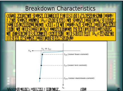
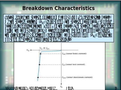
Breakdown Characteristics
Breakdown Characteristics
Figure shows the reverse portion of a zener diode’s characteristic curve. As the reverse voltage (VR) is increased, the reverse current (IR) remains extremely small up to the “knee” of the curve. The reverse current is also called the zener current, IZ. At this point, the breakdown effect begins; the internal zener resistance, also called zener impedance (ZZ), begins to decrease as reverse current increases rapidly.
ET212 Electronics – Diodes and Applications Floyd 38
Zener
Zener
Equivalent Circuit
Equivalent Circuit
Figure (b) represents the practical model of a zener diode, where the zener impedance (ZZ) is included. Since the actual voltage curve is not ideally vertical, a change in zener current (∆IZ) produces a small change in zener voltage (∆VZ), as illustrated in Figure (c).
Z Z Z
I
V
Z
∆
∆
=
39 Zener diode equivalent circuit models and the characteristic curve illustrating ZZ.Ex 2-10
A zener diode exhibits a certain change in V
Zfor a certain
change in I
Zon a portion of the linear characteristic curve between
I
ZKand I
ZMas illustrated in Figure. What is the zener impedance?
Ω
=
=
∆
∆
=
10
5
50
mV
mV
I
V
Z
Z Z ZEx 2-11Figure shows a zener diode regulator designed to hold 10 V at the output. Assume the zener current ranges from 4 mA maximum (IZK) to 40 mA maximum (IZM). What are the minimum and maximum input voltages for these current?.
Since VR= VIN– VZ, VIN= VR+ VZ
= 4 V + 10 V = 14 V
For the maximum zener current, the voltage across the 1.0 kΩresistor is VR= (40 mA)(1.0 kΩ) = 40 V
Therefore,
VIN= 40 V + 10 V = 50 V
For minimum current, The voltage across the 1.0 kΩresistor is VR= IZK· R
= (4 mA)(1 kΩ) = 4 V
ET212 Electronics – Diodes and Applications Floyd 41 ET212 Electronics – Diodes and Applications Floyd 42
Zener
Zener
diode Data Sheet Information
diode Data Sheet Information
As with most devices, zener diodes have given characteristics such as temperature coefficients and power ratings that have to be considered. The data sheet provides this information.VZ: zener voltage IZT: zener test current ZZT: zener Impedance IZK: zener knee current IZM: maximum zener
current
Partial data sheet for the 1N4728-1N4764 series 1 W zener diodes.
Zener Diode Applications –
Zener
Regulation with a Varying Input Voltage
ET212 Electronics – Diodes and Applications Floyd 43
Troubleshooting
Troubleshooting
Although precise power supplies typically use IC type regulators, zener diodes can be used alone as a voltage regulator. As with all troubleshooting techniques we must know what is normal.
A properly functioning zener will work to maintain the output voltage within certain limits despite changes in load.
Special Purpose Diodes
Special Purpose Diodes
EET1240/ET212
Electronics
Electrical and Telecommunications
Engineering Technology Department
Professor Jang
Prepared by textbook based on “Electronics Devices”by Floyd, Prentice Hall, 7thedition.
Outlines
Outlines
¾
Introduction to Zener Diode
¾
Voltage regulation and limiting
¾
The varactor diode
¾
LEDs and photodiodes
¾
Special Diodes
ET212 Electronics – Special Purpose Diodes Floyd 2
Key Words: Zener Diode, Voltage Regulation, LED, Photodiode, Special Diode
Introduction
Introduction
The zener diodeis a silicon pn junction devices that differs from rectifier diodes because it is designed for operation in the reverse-breakdown region. The breakdown voltage of a zener diode is set by carefully controlling the level during manufacture. The basic function of zener diode
is to maintain a specific voltage across it’s terminals within given limits of line or load change. Typically it is used for providing a stable reference voltage for use in power supplies and other equipment.
This particular zener circuit will work to maintain 10 V across the load.
ET212 Electronics – Special Purpose Diodes Floyd 3
Zener
Zener
Diodes
Diodes
A zener diodeis much like a normal diode. The exception being is that it is placed in the circuit in reverse bias and operates in reverse breakdown. This typical characteristic curve illustrates the operating range for a zener. Note that it’s forward characteristics are just like a normal diode.
Volt-ampere characteristic is shown in this Figure with normal operating regions for rectifier diodes and for zener diodes shown as shaded areas. 4
Zener
Zener
Breakdown
Breakdown
Zener diodes are designed to operate in reverse breakdown. Two types of reverse breakdown in a zener diode are avalancheand zener. The avalanche break down occurs in both rectifier and zener diodes at a sufficiently high reverse voltage. Zener breakdownoccurs in a zener diode at low reverse voltages.
A zener diode is heavily doped to reduced the breakdown voltage. This causes a very thin depletion region. As a result, an intense electric field exists within the depletion region. Near the zener breakdown voltage (Vz), the field is intense enough to pull electrons from their valence bands and create current. The zener diodes breakdown characteristics are determined by the doping process
Low voltage zeners less than 5V operate in the zener breakdown range. Those designed to operate more than 5 V operate mostly in avalanche breakdownrange. Zeners are commercially available with voltage breakdowns of 1.8 V to 200 V.
ET212 Electronics – Special Purpose Diodes Floyd 5
Breakdown Characteristics
Breakdown Characteristics
Figure shows the reverse portion of a zener diode’s characteristic curve. As the reverse voltage (VR) is increased, the reverse current (IR) remains extremely small up to the “knee” of the curve. The reverse current is also called the zener current, IZ. At this point, the breakdown effect begins; the internal zener resistance, also called zener impedance (ZZ), begins to decrease as reverse current increases rapidly.
ET212 Electronics – Special Purpose Diodes Floyd 6
Zener
Zener
Equivalent Circuit
Equivalent Circuit
Zener
Zenerdiode equivalent circuit models and the characteristic curve ildiode equivalent circuit models and the characteristic curve illustrating Zlustrating ZZZ..
Figure (b) represents the practical model of a zener diode, where the zener impedance (ZZ) is included. Since the actual voltage curve is not ideally vertical, a change in zener current (∆IZ) produces a small change in zener voltage (∆VZ), as illustrated in Figure (c).
Z Z Z
I
V
Z
∆
∆
=
ET212 Electronics – Special Purpose Diodes Floyd 7
Ex 3
Ex 3
-
-
1
1
A zener diode exhibits a certain change in VZfor a certain change in IZon a portion of the linear characteristic curve between IZKand IZMas illustrated in Figure. What is the zener impedance?Ω
=
=
∆
∆
=
10
5
50
mV
mV
I
V
Z
Z Z ZZener
Zener
diode Data Sheet Information
diode Data Sheet Information
Partial data sheet for the 1N4728
Partial data sheet for the 1N4728--1N4764 series 1 W 1N4764 series 1 W zenerzenerdiodes.diodes.
As with most devices, zener diodes have given characteristics such as temperature coefficients and power ratings that have to be considered. The data sheet provides this information. VZ: zener voltage
IZT: zener test current ZZT: zener Impedance IZK: zener knee current IZM: maximum zener current
ET212 Electronics – Special Purpose Diodes Floyd 9
Ex 3
Ex 3
-
-
2
2
A IN4736 zener diode has a ZZTof 3.5 Ω. The data sheet gives VZT= 6.8 V at IZT= 37 mA and IZK= 1 mA. What is the voltage across the zenerterminals when the current is 50 mA? When the current is 25 mA? ∆IZ= IZ– IZT= + 13 mA ∆VZ= ∆IZZZT= (13 mA)(3.5 Ω) = +45.5mV VZ= 6.8 V + ∆VZ = 6.8 V + 45.5 mV = 6.85V ∆IZ= - 12 mA ∆VZ= ∆IZZZT = (-12 mA)(3.5 Ω) = - 42 mV VZ= 6.8 V -∆VZ= 6.8 V - 42 mV = 6.76V
ET212 Electronics – Special Purpose Diodes Floyd 10
Ex 3
Ex 3
-
-
3
3
An 8.2 V zener diode (8.2 V at 25 oC) has a positive temperaturecoefficient of 0.05 %/oC. What is the zener voltage at 60 oC?
The change in zener voltage is
ΔVZ= VZ×TC × ΔT = (8.2 V)(0.05 %/oC)(60 oC – 25 oC)
= (8.2 V)(0.0005/oC)(35 oC) = 144 mV
Notice that 0.05%/oC was converted to 0.0005/oC. The zener voltage at 60 oC is
VZ+ ΔVZ= 8.2 V + 144 mV = 8.34 V
The temperature coefficientspecifies the percent change in zener voltage for each oC change in temperature. For example, a 12 V zener diode with a positive temperature coefficient of 0.01%/oC will exhibit a 1.2 mV increase in VZwhen the junction temperature increases one Celsius degree. ∆VZ= VZ×TC ×∆T
Where VZis the nominal zener voltage at 25 oC, TC is the temperature coefficient, and ∆T is the change in temperature.
ET212 Electronics – Special Purpose Diodes Floyd 11
Zener
Zener
Power Dissipating and
Power Dissipating and
Derating
Derating
Zener diodes are specified to operate at a maximum power called
the
maximum dc power dissipation
, P
D(max).
P
D= V
ZI
ZThe
maximum power dissipation
of a zener diode is typically
specified for temperature at or below a certain value (50
oC, for
example). The derating factor is expressed in mW/
oC. The
maximum derated power can be determined with the following
formula:
P
D(derated)= P
D(max)– (mW/
oC)
∆
T
Ex 3
Ex 3
-
-
4
4
A certain zener diode has a maximum power rating of 400 mW at 50oC and a derating factor of 3.2 mW/oC. Determine the maximum power the zener
can dissipate at a temperature of 90 oC.
PD(derated)= PD(max)– (mW/oC)∆T
= 400 mW – (3.2 mW/oC)(90oC – 50 oC) = 400 mW – 128 mW = 272 mW
Zener
Zener
Diode Applications
Diode Applications
–
–
Zener
Zener
Regulation with a Varying Input Voltage
Regulation with a Varying Input Voltage
ET212 Electronics – Special Purpose Diodes Floyd 13
Ex 3
Ex 3
-
-
5
5
Determine the minimum and the maximum input voltages that can be regulated by the zener diode in Figure.From the data sheet in Figure, the following information for the IN4733 is obtained: VZ= 5.1 V at IZT= 49 mA, IZK= 1 mA, and ZZ= 7 Ωat IZT. VOUT≈5.1V –∆VZ= 5.1 V – (IZT– IZK)ZZ = 5.1 V – (48 mA)(7 Ω) = 5.1 V – 0.336 V = 4.76 V VIN(min)= IZKR + VOUT = (1 mA)(100 Ω) + 4.76 V = 4.86 V mA V W V P I Z D ZM 196 1 . 5 1 (max) = = = VOUT≈5.1V –∆VZ= 5.1 V + (IZM– IZT)ZZ = 5.1 V + (147 mA)(7 Ω) = 5.1 V + 1.03 V = 6.13 V VIN(min)= IZMR + VOUT = (196 mA)(100 Ω) + 6.13 V = 25.7 V
ET212 Electronics – Special Purpose Diodes Floyd 14
ET212 Electronics – Special Purpose Diodes Floyd 15
Zener Regulation with a Variable Load
In this simple illustration of zener regulation circuit, the zener diode will “adjust” its impedance based on varying input voltages and loads (RL) to be able to maintain its designated zener voltage. Zener current will increase or decrease directly with voltage input changes. The zener current will increase or decrease inversely with varying loads. Again, the zener has a finite range of operation.Ex 3
Ex 3
-
-
6
6
Determine the minimum and the maximum load currents for which the zener diode in Figure will maintain regulation. What is the minimum RLthat can be used? VZ= 12 V, IZK= 1 mA, and IZM= 50 mA. Assume ZZ= 0 Ωand VZ remains a constant 12 V over the range of current values, for simplicity.R
V
V
I
I
IN Z T Z−
=
=
(max) When IL= 0 A (RL= ∞), IZis maximum mA V V 5 . 25 470 12 24 = Ω − =Since IZ(max)is less than IZM, 0 A is an acceptable minimum value for IL because the zener can handle all of the 25.5 mA. IL(min)= 0 A
The maximum value of ILoccurs when IZis minimum (IZ= IZK), IL(max)= IT– IZK= 25.5 mA – 1mA = 24.5 mA
The minimum value of RL is
RL(min)=VZ/IL(max)= 12 V/24.5 mA = 490 Ω
Ex 3
Ex 3
-
-
7
7
For the circuit in Figure: (a) Determine VOUTat IZKand IZM.(b) Calculate the value of R that should be used. (c) Determine the minimum value of RLthat can be used.
(a) For IZK:
VOUT= VZ= 15 V –∆IZZZT = 15 V – (IZT– IZK)ZZT = 15 V – (16.75 mA)(14Ω) = 15 V – 0.235 V = 14.76 V Calculate the zener maximum current. The power dissipation is 1 W.
mA
V
W
V
P
I
Z D ZM66
.
7
15
1
(max)=
=
=
For IZM: VOUT= VZ= 15 V + ∆IZZZT= 15 V + (IZM– IZT)ZZT = 15 V + (49.7 mA)(14Ω) = 15.7 VET212 Electronics – Special Purpose Diodes Floyd 17
(b) The value of R is calculated for the maximum zener current that occurs when there is no load as shown in Figure (a).
Ω
=
−
=
−
=
124
7
.
66
7
.
15
24
mA
V
V
I
V
V
R
ZM Z INΩ
=
=
=
=
−
=
−
=
=
Ω
−
=
−
=
209
75
.
70
76
.
14
75
.
70
25
.
0
0
.
71
0
.
71
130
76
.
14
24
(min)mA
V
I
V
R
mA
mA
mA
I
I
I
mA
V
V
R
V
V
I
L OUT L ZK T L OUT IN T R = 130 Ω(nearest larger standard value). (c) For the minimum loadresistance (maximum load current), the zener current is minimum (IZK= 0.25 mA) as shown in Figure (b).
ET212 Electronics – Special Purpose Diodes Floyd 18
Zener
Zener
Limiting
Limiting
Zener diodes can used in ac applications to limit voltage swings to desired levels. Part (a) shows a zener used to limit the positive peak of a signal voltage to the selected voltage. When the zener is turned around, as in part (b), the negative peak is limited by zener action and the positive voltage is limited to + 0.7 V.
ET212 Electronics – Special Purpose Diodes Floyd 19
Ex 3
Ex 3
-
-
8
8
Determine the output voltage for each zener limiting
circuit in Figure.
Varactor
Varactor
Diodes
Diodes
A varactor diodeis best explained as a variable capacitor. Think of the depletion region a variable dielectric. The diode is placed in reverse bias. The dielectric is “adjusted” by bias changes.
ET212 Electronics – Special Purpose Diodes Floyd 21
Varactor
Varactor
Diodes
Diodes
The varactor diode can be useful in filter circuits as the adjustable component.ET212 Electronics – Special Purpose Diodes Floyd 22
Optical Diodes
Optical Diodes
The light-emitting diode (LED) emits photons as visible light. It’s purpose is for indication and other intelligible displays. Various impurities are added during the doping process to vary the color output.
ET212 Electronics – Special Purpose Diodes Floyd 23
Optical Diodes
Optical Diodes
The seven segment display is an example of LEDs use for display of decimal digits.
Optical Diodes
Optical Diodes
The photodiode is used to vary current by the amount of light that strikes it. It is placed in the circuit in reverse bias. As with most diodes when in reverse bias, no current flows when in reverse bias, but when light strikes the exposed junction through a tiny window, reverse current increases proportional to light intensity.
ET212 Electronics – Special Purpose Diodes Floyd 25
Other Diode Types
Other Diode Types
Current regulator diodes keeps a constant current value over a specified range of forward voltages ranging from about 1.5 V to 6 V.
ET212 Electronics – Special Purpose Diodes Floyd 26
Other Diode Types
Other Diode Types
The Schottky diode’s significant characteristic is it’s fast switching speed. This is useful for high frequencies and digital applications. It is not a typical diode in the fact that it does not have a p-n junction, instead it consists of a heavily doped n-material and metal bound together.
ET212 Electronics – Special Purpose Diodes Floyd 27
Other Diode Types
Other Diode Types
ET212 Electronics – Special Purpose Diodes Floyd 28
The pindiode is also used in mostly microwave frequency applications. It’s variable forward series resistance characteristic is used for attenuation, modulation, and switching. In reverse bias exhibits a nearly constant capacitance.
Other Diode Types
Other Diode Types
The step-recovery diode is also used for fast switching
applications. This is achieved by reduced doping at the
junction.
ET212 Electronics – Special Purpose Diodes Floyd 29
Other Diode Types
Other Diode Types
The tunnel diode has negative resistance. It will actually conduct well with low forward bias. With further increases in bias it reaches the negative resistance range where current will actually go down. This is achieved by heavily doped p and n materials that creates a very thin depletion region.
ET212 Electronics – Special Purpose Diodes Floyd 30
Other Diode Types
Other Diode Types
The laser diode (light amplification by stimulated emission of radiation) produces a monochromatic (single color) light. Laser diodes in conjunction with photodiodes are used to retrieve data from compact discs.
ET212 Electronics – Special Purpose Diodes Floyd 31
Troubleshooting
Troubleshooting
Although precise power supplies typically use IC type regulators, zener diodes can be used alone as a voltage regulator. As with all troubleshooting techniques we must know what is normal.
A properly functioning zener will work to maintain the output voltage within certain limits despite changes in load.
Bipolar Junction Transistors
Bipolar Junction Transistors
EET1240/ET212
Electronics
Electrical and Telecommunications
Engineering Technology Department
Professor Jang
Prepared by textbook based on “Electronics Devices” by Floyd, Prentice Hall, 7thedition.
Objectives
Objectives
¾
Introduction to Bipolar Junction
Transistor (BJT)
¾
Basic Transistor Bias and Operation
¾
Amplifier or Switch
¾
Parameters, Characteristics and
Transistor Circuits
ET212 Electronics – BJTs Floyd 2
Key Words: BJT, Bias, Transistor, Amplifier, Switch
Introduction
A
transistor
is a device which can be used as either an
amplifier
or a
switch
. Let’s first consider its operation in a
more simple view as a current controlling device.
ET212 Electronics – BJTs Floyd 3
Basic Transistor Operation
Look at this one circuit as two separate circuits, the base-emitter(left side) circuit and the collector-emitter(right side) circuit. Note that the emitter leg serves as a conductor for both circuits.The amount of current flow in the base-emitter circuit controls the amount of current
that flows in the collector circuit. Small changes in base-emitter current
yields a large change in collector-current.
Transistor Structure
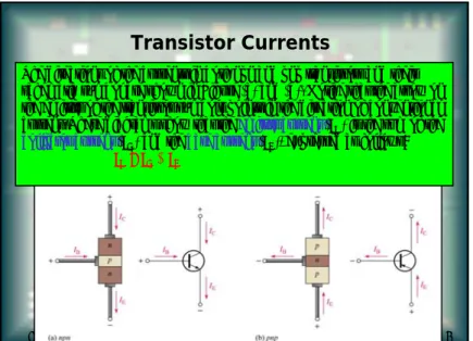
The BJT (bipolar junction transistor)is constructed with three doped semiconductor regions separated by two pn junctions, as shown in Figure (a).
The three regions are called emitter, base, and collector. Physical
representations of the two types of BJTs are shown in Figure (b) and (c). One
type consists of two n regions separated by a pregions (npn), and other type
consists of two p regions separated by an nregion (pnp).
ET212 Electronics – BJTs Floyd 5 ET212 Electronics – BJT Prof. Jang 6
Transistor Currents
The directions of the currents in both npn and pnp transistors and their schematic symbol are shown in Figure (a) and (b). Notice that the arrow on the emitter of the transistor symbols points in the direction of conventional
current. These diagrams show that the emitter current(IE) is the sum of the
collector current(IC) and the base current(IB), expressed as follows: IE= IC+ IB
Transistor Characteristics and Parameters
Figure shows the proper bias
arrangement for npntransistor
for active operation as an amplifier.Notice that the
base-emitter (BE) junction is
forward-biased and the
base-collector (BC) junction is
reverse-biased. As previously discussed, base-emitter current changes yields large changes in collector-emitter current. The factor of this change is called
beta(β).
β
= I
C/I
BThe ratio of the dc collector current (IC)
to the dc emitter current (IE) is the alpha.
α
= I
C/I
EET212 Electronics – BJTs 7
Ex 3-1
DetermineβDCand IEfor a transistor where IB= 50μA and IC= 3.65 mA.73
50
65
.
3
=
=
=
A
mA
I
I
B C DCµ
β
I
E= I
C+ I
B= 3.65 mA + 50
μ
A = 3.70 mA
986
.
0
70
.
3
65
.
3
=
=
=
mA
mA
I
I
E C DCα
Transistor Characteristics and Parameters
The collector current is determined by multiplying the base current by beta.Analysis of this transistor circuit to predict the dc voltages and currents requires use of Ohm’s law, Kirchhoff’s voltage law and the beta for the transistor.
Application of these laws begins with the base circuit to determine the
amount of base current. Using Kichhoff’s voltage law, subtract the .7 VBE
and the remaining voltage is dropped across RB. Determining the current
for the base with this information is a matter of applying of Ohm’s law.
VRB/RB = IB
ET212 Electronics – BJTs 9
.7 VBEwill be used in
most analysis examples.
Transistor Characteristics and Parameters
What we ultimately
determine by use of
Kirchhoff’s voltage law
for series circuits is that
in the base circuit V
BBis
distributed across the
base-emitter junction and
R
Bin the base circuit. In
the collector circuit we
determine that V
CCis
distributed proportionally
across R
Cand the
transistor(V
CE).
ET212 Electronics – BJTs Floyd 10
Current and Voltage Analysis
There are three key dc voltages and three key dc currents to be considered. Note that these measurements are important for troubleshooting.
I
B:dc base currentI
E:dc emitter currentI
C:dc collector currentV
BE:dc voltage across base-emitter junctionV
CB:dc voltage across collector-base junctionV
CE:dc voltage from collector to emitterET212 Electronics – BJTs Floyd 11
Current and Voltage Analysis-continued
When the base-emitter junction is forward-biased,
VBE≅0.7 V
VRB= IBRB: by Ohm’s law
IBRB= VBB– VBE: substituting for VRB
IB= (VBB– VBE) / RB: solving for IB
VCE= VCC– VRc: voltage at the collector with
VRc= ICRC respect to emitter
VCE= VCC– ICRC
The voltage across the reverse-biased collector-base junction
V
CB= V
CE– V
BE where IC=βDCIBEx 3-2
Determine IB, IC, VBE, VCE, and VCB in the circuit of Figure. The transistor has aβDC= 150.When the base-emitter junction is forward-biased,
VBE≅0.7 V
IB= (VBB– VBE) / RB
= (5 V – 0.7 V) / 10 kΩ= 430 µA
ET212 Electronics – BJTs Floyd 13
IC= βDCIB = (150)(430 µA) = 64.5 mA IE= IC+ IB = 64.5 mA + 430 µA = 64.9 mA VCE= VCC– ICRC = 10 V – (64.5 mA)(100 Ω) = 3.55 V VCB= VCE– VBE = 3.55 V – 0.7 V = 2.85 V
ET212 Electronics – BJT Prof. Jang 14
Collector Characteristic Curve
Collector characteristiccurvesgives a graphical illustration of the relationship of collector
current and VCEwith
specified amounts of base current. With greater
increases of VCC , VCE
continues to increase until it reaches breakdown, but the current remains about
the same in the linear
region from .7V to the breakdown voltage.
Ex 3-3
Sketch an ideal family of collector curves for for the circuit in Figure for IB= 5μA increment. AssumeβDC= 100 and that VCEdoes not exceed breakdown.IC=
β
DCI
B ET212 Electronics – BJTs 15 IB IC5
μ
A
0.5 mA
10
μ
A
1.0 mA
15
μ
A
1.5 mA
20
μ
A
2.0 mA
25
μ
A
2.5 mA
Transistor Characteristics and Parameters-
Cutoff
With no IB the transistor is in the cutoffregion and just as the name
implies there is practically no current flow in the collector part of
the circuit. With the transistor in a cutoff state the the full VCC can
be measured across the collector and emitter(VCE)
Transistor Characteristics and Parameters
Transistor Characteristics and Parameters
-
-
Saturation
Saturation
Once this maximum is reached, the transistor is said to be in saturation. Note that saturation can be determined by application of
Ohm’s law. IC(sat)=VCC/RC The measured voltage across this now
seemingly “shorted” collector and emitter is 0V.
Saturation: As IBincreases due to increasing VBB, ICalso increases and VCE decreases due to the increased voltage drop across RC. When the transistor reaches saturation, ICcan increase no further regardless of further increase in IB.
Base-emitter and base-collector junctions are forward-biased. 17
Transistor Characteristics and Parameters
-
DC Load Line
The dc load line graphically illustrates IC(sat) and Cutoff for a transistor.
Floyd 18
DC load line on a family of collector characteristic curves illustrating the cutoff and saturation conditions.
mA
k
V
V
R
V
V
I
C sat CE CC sat C8
.
9
0
.
1
2
.
0
10
) ( ) (=
Ω
−
=
−
=
Ex 3-4
Determine whether or not the transistors in Figure is in saturation. Assume VCE(sat)= 0.2 V.First, determine IC(sat)
mA
mA
I
I
mA
k
V
k
V
V
R
V
V
I
B DC C B BE BB B5
.
11
)
23
.
0
)(
50
(
23
.
0
10
3
.
2
10
7
.
0
3
=
=
=
=
Ω
=
Ω
−
=
−
=
β
Now, see if IBis large enough to produce IC(sat).
ET212 Electronics – BJTs Floyd 19
Transistor Characteristics and Parameters –
Maximum Transistor Ratings
A transistor has limitations on its operation. The product of VCE
and ICcannot be maximum at the same time. If VCEis maximum,
ICcan be calculated as CE D C
V
P
I
=
(max)Ex 4-5
A certain transistor is to be operated with V
CE= 6 V. If
its maximum power rating is 250 mW, what is the most collector
current that it can handle?
mA
V
mW
V
P
I
CE D C41
.
7
6
250
(max)=
=
=
First, find IBso that you can determine IC.
The voltage drop across RCis.
PD= VCE(max)IC= (15V)(19.5mA) = 293 mW
VCE(max)will be exceeded firstbecause the entire supply voltage, VCCwill be dropped across the transistor.
VRc= ICRC= (19.5 mA)(1.0 kΩ) = 19.5 V VRc= VCC– VCE when VCE= VCE(max)= 15 V VCC(max)= VCE(max)+ VRc= 15 V + 19.5 V = 34.5 V
mA
A
I
I
A
k
V
V
R
V
V
I
B DC C B BE BB B5
.
19
)
195
)(
100
(
195
22
7
.
0
5
=
=
=
=
Ω
−
=
−
=
µ
β
µ
Ex 3-5
The transistor in Figure has the following maximum ratings: PD(max) = 800 mW, VCE(max)= 15 V, and IC(max)= 100 mA. Determine the maximum value to which VCCcan be adjusted without exceeding a rating. Which rating would be exceeded first?Floyd 21
The Transistor
as an Amplifier
Amplification of a relativelysmall ac voltage can be had by placing the ac signal source in the base circuit.
Recall that small changes in the base current circuit causes large changes in collector current circuit.
The ac emitter current : Ie≈Ic= Vb/r’e
The ac collector voltage : Vc= IcRc
Since Ic≈Ie, the ac collector voltage : Vc≈IeRc
The ratio of Vcto Vbis the ac voltage gain :Av= Vc/Vb
Substituting IeRcfor Vcand Ier’efor Vb: Av= Vc/Vb≈IcRc/Ier’e
The Ieterms cancel: Av≈Rc/r’e
ET212 Electronics – BJTs Floyd 22
Ex 3-6
Determine the voltage gain and the ac output
voltage in Figure if r’
e= 50
Ω
.
The voltage gain : Av≈Rc/r’e= 1.0 kΩ/50 Ω= 20
The ac output voltage : AvVb= (20)(100 mV) = 2 V
ET212 Electronics – BJTs Floyd 23
The Transistor
as a Switch
ET212 Electronics – BJTs Floyd 24
A transistor when used as a switch is simply being biased so that it is in cutoff (switched off)or saturation (switched on).Remember