Accelerating BLAS on Custom Architecture
through Algorithm-Architecture Co-design
Farhad Merchant, Tarun Vatwani, Anupam Chattopadhyay,
Senior Member, IEEE,
Soumyendu Raha,
S K Nandy,
Senior Member, IEEE,
and Ranjani Narayan
Abstract—Basic Linear Algebra Subprograms (BLAS) play key role in high performance and scientific computing applications.
Experimentally, yesteryear multicore and General Purpose Graphics Processing Units (GPGPUs) are capable of achieving up to 15 to 57% of the peak performance at 65W to 240W of power respectively in underlying platform for compute bound operations like Double/Single Precision General Matrix Multiplication (XGEMM) while for bandwidth bound operations like Single/Double precision Matrix-vector Multiplication (XGEMV) it is merely 5 to 7% respectively. Achieving performance for BLAS requires moving away from conventional wisdom and evolving towards customized accelerator tailored for BLAS. In this paper, we present acceleration of Level-1 (vector operations), Level-2 (matrix-vector operations), and Level-3 (matrix-matrix operations) BLAS through algorithm architecture co-design on a Coarse-grained Reconfigurable Architecture (CGRA). We choose REDEFINE CGRA as a platform for our experiments since REDEFINE can be adapted to support domain of interest through tailor-made Custom Function Units (CFUs). For efficient sequential realization of BLAS, we present a design of a Processing Element (PE) that can achieve up-to 74% of the peak performance of the PE for DGEMM, 40% for DGEMV and 20% for DDOT. We attached this PE to the REDEFINE CGRA as a CFU and show the scalibilty of our solution. Finally, we show performance improvement of 3-140x in PE over commercially available Intel
micro-architectures, ClearSpeed CSX700, FPGA, and Nvidia GPGPUs.
Index Terms—Parallel computing, dense linear algebra, multiprocessor system-on-chip, instruction level parallelism
F
1
I
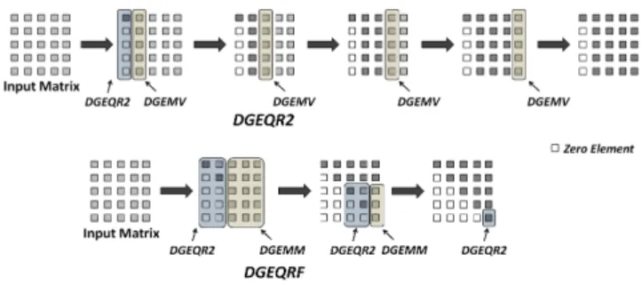
NTRODUCTIONSeveral engineering and scientific applications require solution of dense linear systems of equations and linear least square problems where matrix factorizations like LU, QR and Cholesky methods play pivotal role. Traditionally, routines of these factorizations that are part of Linear Algebra Package (LAPACK) are written as a series of Basic Linear Algebra Subprogram (BLAS) calls [1][2]. Pictorial representation of double precision QR factorization rou-tines, DGEQR2 and DGEQRF that are part of LAPACK is shown in the figure 1.
Fig. 1: DGEQR2 and DGEQRF Routines
• Farhad Merchant and Anupam Chattopadhyay are with School of
Com-puter Science and Engineering, Nanyang Technological University, Singa-pore
E-mail:{mamirali,anupam}@ntu.edu.sg
• Tarun Vatwani is with Indian Institute of Technology, Jodhpur
• Soumyendu Raha and S K nandy are with Indian Institute of Science,
Bangalore
• Ranjani Narayan is with Morphing Machines Pvt. LTd.
Manuscript received October 20, 2016;
In the pictorial representation of DGEQR2 it can be ob-served that DGEQR2 is dominated by matrix-vector operations (DGEMV in BLAS) and DGEQRF is dominated by DGEQR2 and matrix-matrix operations (DGEMM in BLAS). Our experi-ments for DGEQR2 on Intel Core i7 and observation using Intel VTune™ suggests that for matrix of size 10k×10k, 99% of the total time DGEMV executes while DDOT executes for hardly 1% of the total time of the operation of DGEQR2. Similarly, DGEQRF is dominated by DGEMM and it runs for 99% of the total time of DGEQRF while DGEQR2 runs for 1% of the time. Similar observations can be made in the routines like XGETRF (double/single precision LU factorization routine) and XPBTRF (double/single precision Cholesky factorization routine). Considering importance of BLAS in LAPACK, it is arguably one of the most interesting research problem to accelerate BLAS.
For acceleration of BLAS, a library based approach is adopted. Based on reference BLAS and LAPACK available on Netlib, Intel Math Kernel Library (MKL), IBM’s Engineering and Scientific Subroutine Library (ESSL), AMD’s AMD Core Math Library (ACML), Nvidia’s CUDA Linear Algebra (CULA) where CULA dense is for Dense Linear Algebra (DLA) and CULA sparse is for Sparse Linear Algebra (SLA), and cuBLAS which is yet another CUDA Baic Linear Algebra Subprograms are developed. There are also several open source packages for multore and Graphics Processing Unit (GPU) based realizations like Parallel Linear Algebra Software for multicore Architectures (PLASMA) and Matrix Algebra on Multicore and GPU Architectures (MAGMA) use BLAS as a basic building block. All these mentioned packages are developed for multicore and GPUs for realization of DLA computations in the most efficient way. PLASMA and MAGMA incorporate tiled algorithms that are capable of exploiting memory hierarchy efficiently [3][4]. Despite all the efforts being directed
towards acceleration of DLA computations, the performance at-tained by yesteryear platforms is as low as 15-17% of the peak performance in multicore and 55-57% of the peak performance
in GPU at ≥65W and≥240W power consumption respectively.
Considering inability of GPU and multicore architectures in ex-ploiting parallelism available in BLAS, we recommend algorithm-architecture co-design for BLAS as a solution for efficient realiza-tion of DLA.
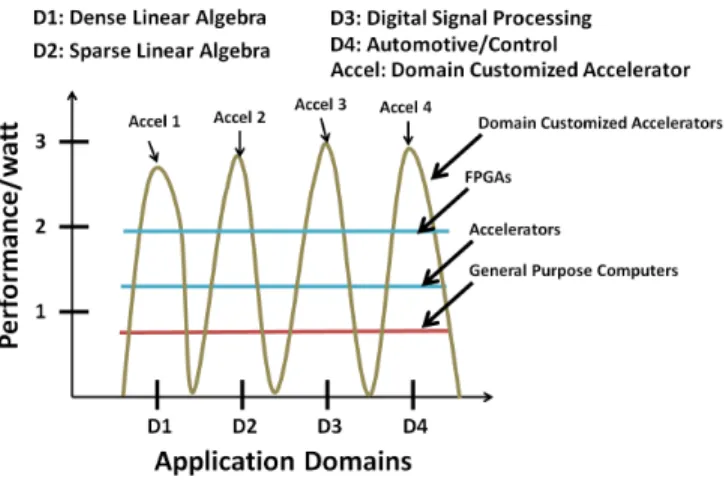
Fig. 2: Performance of Domain Customized Accelerators, FPGAs, Multicore, and General Purpose Accelerators (GPGPUs)
Recently, Coarse-grained Reconfigurable Architectures
(CGRAs) have gained popularity due to their power performance and flexibility. Performance advantage in CGRAs is attained by supporting selected number of paths out of all possible data-paths and hence they occupy middle ground between Application Specific Integrated Circuits (ASICs) and Field Programmable Gate Arrays (FPGAs) [5][6]. Figure 2 depicts performance of different accelerators (Accel 1, Accel 2,...) which are instances of a CGRA. CGRAs like REDEFINE have special feature that they can be customized for application domains where several data-paths belonging to a particular domain of interest are realized as a reconfigurable ASIC. In REDEFINE, several tiles are connected through a Network-on-Chip (NoC) where Custom Function Units (CFUs) tailored for a particular domain decides performance of overall system for application domain [7][8].
Major contributions in this paper are as follows:
• Firstly, we present realization of legacy BLAS on off-the-shelf Intel/AMD processor and Nvidia GPUs. We present Cycles-per-Instruction (CPI) and Gflops/watt (Giga flops per watt) based analysis for implementation on Intel, AMD and Nvidia GPU and mention shortcomings in the performance achieved
• We present Directed Acyclic Graph (DAG) based analysis of representative routines of Level-1, Level-2, and Level-3 BLAS and exhibit available parallelism and possible data locality. Based on our analysis, we arrive at design of a Processing Element (PE)
• Several architectural enhancements are performed in the PE for improving throughput of BLAS by exploiting ex-hibited parallelism. These enhancements result in efficient realization of sequential BLAS in the PE. It is shown that through algorithm-architecture co-design, we are able to break the saturation point and improve the overall
performance of the BLAS in PE. With each enhancement, we show that we are able to push the saturation point towards theoretical peak performance of the PE at very high energy efficiency
• We attach the PE to the Routers in REDEFINE for parallel realization of BLAS and show algorithmic and architecture scalability
The organization of the paper is as follows: In section 2, some of the recent Multi-core, GPU, and custom realizations of BLAS are discussed. In section 3, we present legacy BLAS realization on multicore and GPU and CPI and energy efficiency analysis of the realization. In section 4, DAG based analysis of Level-1, Level-2, and Level-3 BLAS is presented and we derive preliminary specifications of a PE. Architectural enhancements in the PE for improvement in throughput in BLAS and parallel realization of BLAS on REDEFINE where we attach PE as a CFU to REDEFINE are presented in section 5 and the work is summarized in section 6.
2
R
ELATEDW
ORKOver the years there have been several efficient realization of BLAS due to applicability in high performance scientific appli-cation. In this section, we survey several multicore and GPU based, and custom realizations of BLAS. We consider FPGA based realizations as custom realizations.
2.1 Software Packages for Multicore Platforms
The first ever software library LINPACK for performing linear algebra computations was developed in 1970s and early 1980s [9]. Subsequently, LINPACK that used Level-1 BLAS as a basic building block was superseded by LAPACK that uses Level-3 BLAS as a basic building block [2]. In the recent years, with arrival of multicore architectures, there have been several advancements in the parallel realization of LAPACK. One such effort is PLASMA, that can perform computations on multicore architecture with the help of dynamic scheduler Queuing and Runtime for Kernels (QUARK). PLASMA creates pipeline model for parallel execution by dynamic scheduling of BLAS kernels on the multicore platform [10][3]. A Formal Linear Algebra Method Environment (FLAME) focuses on issues related to programming of linear algebra programs. The focus of the FLAME project is to automatically generate efficient linear algebra codes for the underlying platform [11][12]. Under the umbrella of FLAME project, BLAS-like Library Instantiation Software (BLIS) focuses on rapid scheduling of BLAS-like kernels on multicore architec-tures. Automatically Tuned Linear Algebra Software (ATLAS) is an matured open source package that generates BLAS for the underlying platform [13][14]. ATLAS relies on legacy BLAS for generation of efficient code for the underlying platform where several parameters are tweaked to suit the underlying platform. OpenBLAS is another open source package that focuses on efficient realization of DLA computations [15][16]. OpenBLAS relies on GotoBLAS for the performance where GotoBLAS is a set of assembly programs written for DLA computations. A major shortcoming of the packages like LAPACK, PLASMA, BLIS, ATLAS, and OpenBLAS is lack of support from the underlying platform resulting in 15-20% of the theoretical peak performance.
2.2 GPU Based Realizations
GPUs were original designed for graphics processing are highly suitable for general purpose computing. There have been several packages developed to perform efficient BLAS functionality on GPUs. The most prominent of all of them is MAGMA software package [4]. MAGMA relies on MAGMA BLAS for the perfor-mance where the perforperfor-mance of MAGMA DGEMM is observed to be 57% of the peak performance of Tesla C2050 GPU with the-oretical peak of 512 Gflops for double precision. KAUST BLAS (KBLAS) is one of the most recent and ongoing research project at KAUST. KBLAS internally relies on Cuda BLAS developed by Nvidia for the performance on GPU. BLASX presented in [17] focuses on optimizaiton of Level-3 BLAS in multi-GPU en-vironment. BLASX minimizes the global communication through two level hierarchical tile cache structures and achieves 92.68% of the in-core cuBLAS DGEMM. BLASX also contains better load balancing techniques compared to MAGMA and cuBLAS. Despite elegant scheduling technique and efficient exploitation of memory hierarchy BLASX, the performance achieved by BLASX is limited by cuBLAS DGEMM. In [18], requirement for cache memory is studied in detail for achieving superliear speed-up for XGEMM. The study presented in [18] has no mention of data type if it is single precision or double precision. All the GPU based realization of BLAS fail to achieve high performance due to lack of support for GEMM primitives.
2.3 Custom Realizations
Customized accelerators are the class of architectures that are tuned for low energy, and unit area at high throughput for domain of interest [19][20][21][22]. Cell Broadband Engine (CBE) from International Business Machine (IBM) is a high performance architecture designed based on Power PC core [23]. Due to energy efficiency of CBE, it is viewed as an ideal platform for scientific computing [24]. ClearSpeed’s CSX architecture is back bone of ClearSpeed CSX600 and CSX700 processors. These processors have very high energy efficiency and operate at 12 Watts with theoretical peak of 96 GFlops [25][26][20]. A major shortcoming of ClearSpeed’s CSX and CBE architectures are low Gflops/W and Gflops/mm2[20].
There have been several attempts in viewing Field Pro-grammable Gate Arrays (FPGAs) as high performance computing engines [27][28][29]. Mostly FPGAs are envisioned as a high performance co-processor of a programmable host processor for compute intensive applications [30][31]. A major disadvantage of FPGAs is higher power consumption than an Application Specific Integrated Circuit (ASIC) counterpart of the same logic. FPGAs are also limited by the on-chip logic resulting in scalability issues in high performance computing applications.
To overcome shortcomings of the existing architectures in exploiting parallelisms available in DLA computations, we take a route of algorithm-architecture co-design where we ensure high performance along with energy, area efficiency, and scalability.
3
BLAS R
EALIZATION ONO
FF-
THE-
SHELFP
RO-CESSORS
GEMM (Level-3 BLAS) and GEMV (Level-2 BLAS) are the most prominent routines in many engineering and scientific computa-tions. These routines also have pedagogical importance due to its
simplistic nature and often used to evaluate emerging architec-tures. In this section, first we discuss GEMM algorithm and then we examine some of the recent realization of GEMM. Based on the anslysis of the profiling of the algorithm, we arrive at the pitfalls in extracting performance out of GEMM on contemporary multicore and GPU platforms.
3.1 GEMM and GEMV Algorithms
Algorithm 1GEMM - General Matrix Multiplication
1: Allocate memories for input and output matrices and initialize input matrices
2: fori= 1tomdo
3: forj = 1tondo
4: fork= 1tondo
5: C(i,j) = A(i,k)B(k,j) + C(i,j)
6: end for
7: end for
8: end for
Algorithm 2GEMV - Matrix Vector Multiplication
1: Allocate memories for input matrix, input vector and output vector. Initialize input matrix and input vector
2: forj= 1tondo
3: fori= 1tomdo
4: y(i) = A(i,j)x(j) + y(i)
5: end for
6: end for
Pseudo codes for GEMM and GEMV are described in algo-rithms 1 and 2 respectively. GEMM algorithm has three loops and hence it belongs to Level-3 BLAS while GEMV belongs to Level-2 BLAS. For multiplying two matrices of size n×n, it takesn3multiplications andn3−n2additions while GEMV takes n2 multiplications andn2−nadditions. Typically, GEMM and
GENV exhibit Instruction Level Parallelism (ILP) and Data Level Parallelism (DLP). GEMM also exhibits mighty data locality and is capable of sustaining O(n) computations to communication ratio. All together, if exploited efficiently and accelerated, GEMM and GEMV become an ideal candidate to be used as a basic building block for many high performance scientific applications. Since, GEMM has three nested loops, these loops can be permuted to change the access pattern of input matrices as shown in table 1.
TABLE 1: General Matrix Multiplication (GEMM): Loop Orderings and Access Patterns
Loop Order
Inner Loop
Middle Loop Inner Loop Data Access
ijk dot vector×matrix A by row, B by column jik dot matrix×vector A by row, B by column ikj saxpy rowgaxpy B by row, C by row jki saxpy columngaxpy A by column, C by column kij saxpy row outer product B by row, C by row kji saxpy column outer product A by column, B by column
In the table 1, saxpy stands for ”scalar a multiplied by vectorxplus vectory” andgaxpystands for generalizedsaxpy
3.2 Performance Evaluation of GEMM and GEMV
For contemporary architecture, highly efficient GEMM is realized as a subroutine in BLAS. There exists several vendor specific realizations of DGEMM. For our experiments, we take DGEMM available in BLAS from The Netlib and for evaluation on GPU we use MAGMA DGEMM. We compile DGEMM for different Intel and AMD machines with different compiler options and evaluate the performance of DGEMM for these architectures. We evaluate MAGMA DGEMM on Telsa C2050.
Figure 3(a) depicts CPI of DGEMM when executed on Intel Haswell and AMD Bulldozer micro-architectures. For experimen-tal results shown in figure 3(a), we have used BLAS and CBLAS1 available in The Netlib and hence we have compiled BLAS and CBLAS using publicly available gf ortran and gcc. It can be observed in figure 3(a) that the CPI in the DGEMM saturates at around 0.85 for Intel’s Haswell and AMD’s Bulldozer. For the matrices that fit in the L1 cache achieve CPI that is lower than that for the matrices that do not fit in theL1 cache. This is due toL1 cache misses observed for larger matrices. While for the matrices that do not fit in the cache memory, attained CPI is slightly higher than the smaller matrices2. For Intel Haswell and AMD Bulldozer, the lower bound of the CPI is0.0625. It can be observed that with DGEMM, which is highly optimized routine of BLAS, CPI achieved is nowhere close to the lower bound of CPI of the architecture. Similar trend is observed when we consider Gflops as a performance metric as shown in figure 3(b).
It can be observed in the figure 3(b) that, for the matrices that fit in the cache memory, the Gflops attained is higher. For the larger matrices that do not fit in the cache memory, Gflops decreases due to cache misses. While these architectures have peak performance of48Gflops, attained performance is 10-11% of the peak performance.
One way to improve performance is to use the vendor specific compilers, since vendor specific compilers perform architecture aware optimizations in the programs. In order to further push the performance of DGEMM on Intel Haswell micro-architecture we use Intel C Compiler (icc) for compiling DGEMM routine in BLAS. Performance improvement in CPI and Gflops is shown in figures 3(c) and 3(d) respectively.
It can be observed in the figures 3(c) and 3(d) that the performance improvement in DGEMM is still far from the lower bound of the CPI and peak Gflops.
In the next set of experiments, we add −mavx compiler
switch while compiling withicc. Performance improvement due to these switches is shown in the figure 3(e) and figure 3(f).
It can be observed from figures 3(e) and 3(f) that compiler switch−mavximproves performance and finally we are able to achieve 15-17% of the peak IPC (or CPI) and peak Gflops for DGEMM. Percentage of peak performance achieved is 4-5% for DGEMV and 55-57% for DGEMM in Tesla C2050 as depicted in figure 3(g) while percentage of peak performance achieved in Intel and Nvidia machines for DGEMV and DGEMM is ranging from 5% to 57% as shown in the figure 3(h). Considering Gfops/watt as a performance parameter, DGEMV and DGEMM in the BLAS achieve performance of 0.14 Gflops/watt and 0.25 Gflops/watt respectively while MAGMA DGEMV and MAGMA DGEMM achieve performance of 0.03 Gflops/watt to 0.225 Gflops/watt
re-1. CBLAS consists of C wrappers written around BLAS where BLAS is written in Fortran
2. Just to re-emphasize: In case of CPI, lower the better
spectively as shown in figure 3(i). One more observation we make from the figure 3(e) and VTune™ that use of−mavxcompiler switch along withiccreduces number of instructions by half. This is because of use of FMA instructions in the generated assembly code. Reduction in the number of instructions leads to increase in CPI measured by VTune™. Though, there is an increase in CPI, performance in terms of Gflops is observed to be improved as shown in the figure 3(f). Hence, CPI measured by VTune™can not be considered as a correct measure for performance. We define terms Cycles-per-Flops (CPF) to be used instead CPI and Flops-per-Cycle (FPC) to be used instead IPC as follows:
CP F = T otal N umber of Clock T icks
T otal N umber of F loating P oint Operations
(1) We define FPC as follows:
F P C= 1
CP F (2)
CPF and FPC help us to evaluate performance of the ar-chitectures and algorithms more effectively. This is because the granularity of the compute resources considered in CPF and FPC is at the level of floating point operation and not at the level of Fused Multiply-add (FMA).
Across the experiments, we can observe that, significant efforts are needed to improve the performance of DGEMV and DGEMM on contemporary architectures. While there is a minimal support from the programming model and lack of domain specific archi-tectural features in the architecture model, achieving satisfactory performance is not possible. We address this challenge of ex-tracting performance from DLA computations through algorithm-architecture co-design in the subsequent sections of this paper.
4
A
NALYSIS OFBLAS
ANDCFU
In this section, we present graph based analysis of several Level-1, Level-2, and Level-3 BLAS. We choose several representative routines in all three levels of BLAS3.
4.1 Vector Operations (Level-1 BLAS)
Level-1 BLAS typically hasO(n)operations for a vector size of
nand data movement required is also O(n). We analyzeddot,
dnrm2, and daxpy operations here. Figure 4 represents inner product of two vectors given by equation 3.
c=xTy (3) wherex= a11 a12 a13 .... a1n , andy= b11 b21 b31 . . . .bn1 . DAG
forddotis shown in figure 4 forn= 8.
The routineddothas application in vector and matrix-matrix multiplication.
3. Due to availability of double precision floating point unit, we consider
only routines that are with prefix ”d”. For example first ”d” inddotrepresents
1x1 2x2 3x3 4x4 5x5 6x6 7x7 8x8 9x9 10x10 0.65 0.7 0.75 0.8 0.85 0.9
0.95 CPI (Intel Core i7 4th Gen)
CPI (Intel Core i5 4th Gen) CPI (AMD FX 8150) Matrix Size C P I X 103
(a) CPI in DGEMM on Intel Haswell and AMD Bulldozer Micro-architectures
1x1 2x2 3x3 4x4 5x5 6x6 7x7 8x8 9x9 10x10 4.3 4.35 4.4 4.45 4.5 4.55 4.6 4.65
Gflops (Intel Core i7 4th Gen) Gflops (Intel Core i5 4th Gen) Gflops (AMD FX 8150) Matrix Size G fl o p s X 103
(b) Gflops in DGEMM on Intel Haswell and AMD Bulldozer Micro-architectures
1x1 2x2 3x3 4x4 5x5 6x6 7x7 8x8 9x9 10x10 0.63 0.63 0.63 0.63 0.63 0.64 0.64 0.64 0.64
CPI (Intel Core i7 4th Gen) CPI (Intel Core i5 4th Gen)
Matrix Size
C
P
I
X 103
(c) CPI in DGEMM on Intel Haswell
Micro-architecture withicc
1x1 2x2 3x3 4x4 5x5 6x6 7x7 8x8 9x9 10x10 4 4.2 4.4 4.6 4.8 5 5.2 5.4
Gflops (Intel Core i7 4th Gen) Gflops (Intel Core i5 4th Gen)
Matrix size G fl o p s X 103
(d) Gflops in DGEMM on Intel Haswell
Micro-architecture withicc
1x1 2x2 3x3 4x4 5x5 6x6 7x7 8x8 9x9 10x10 0.37 0.37 0.37 0.38 0.38 0.38 0.38 0.38
CPI (Intel Core i7 4th Gen) CPI (Intel Core i5 4th Gen)
Matrix Size
C
P
I
X 103
(e) CPI in DGEMM on Intel Haswell
Micro-architecture withiccand−mavx
compiler switches 1x1 2x2 3x3 4x4 5x5 6x6 7x7 8x8 9x9 10x10 8.4 8.41 8.42 8.43 8.44 8.45 8.46 8.47 8.48 8.49
Gflops (Intel Core i7 4th Gen) Gflops (Intel Core i5 4th Gen)
Matrix Size G fl o p s X 103
(f) Gflops in DGEMM on Intel Haswell
Micro-architecture withiccand−mavx
compiler switches 1x1 2x2 3x3 4x4 5x5 6x6 7x7 8x8 9x9 10x10 0 50 100 150 200 250 300 350 MAGMA_DGEMV MAGMA_DGEMM Matrix Size G fl o p s X 103
(g) Gflops in MAGMA DGEMM and
MAGMA DGEMV on Nvidia Tesla
C2050 1x1 2x2 3x3 4x4 5x5 6x6 7x7 8x8 9x9 10x10 0 10 20 30 40 50 60
70 DGEMM (Intel Core i7) DGEMV (Intel Core i7) DGEMM (Tesla C2050) DGEMV (Tesla C2050) Matrix Size P e rc e n ta g e o f P e a k P e rf o rm a n c e X 103 (h) Gflops in DGQMV,
DGEMM, MAGMA DGEMM and
MAGMA DGEMV 1x1 2x2 3x3 4x4 5x5 6x6 7x7 8x8 9x9 10x10 0 0.05 0.1 0.15 0.2 0.25 0.3
DGEMM (Intel Core i7) DGEMV (Intel Core i7) DGEMM (Tesla C2050) DGEMV (Tesla C2050)
Matrix Size G fl o p s /W a tt X 103
(i) Gflops/watt in DGEMV,
DGEMM, MAGMA DGEMM and
MAGMA DGEMV on Nvidia Tesla
C2050
Fig. 3: Performance of DGEMV and DGEMM on Different Micro-architectures
Fig. 5: DAG of DGEMV forn= 4
dnrm2is given by equation 4 and DAG fordrnm2is shown in figure 4. k= √ xTx= q a2 11+a212+...+a21n (4)
daxpy is given by equation 5 and DAG for daxpy is given figure 4
y=αx+y (5)
It can be observed from the DAGs of ddotanddnrm2 that the DAGs of these two routines are similar except presence of square root indnrm2routine.dnrm2can be realized with same multiplier and adder resources asddot. It can also be observed in the figure 4 that the first level in the DAGs is multiplication and all these multiplications can potentially be executed in parallel. The next levels of DAGs ofddotanddnrm2are additions. Additions in each level of DAGs can be performed simultaneously if the inputs are available.
4.2 Matrix-vector Operations (Level-2 BLAS)
Matrix-vector operations are typicallyO(n2)for input matrix of sizen×nand vector of sizenand data movement required is also
O(n2). In our analysis we consider double precision matrix-vector
multiplication (DGEMV) routine of BLAS. DGEMV is given in equation 6.
y=Ax+y (6)
where A is a matrix of size n×n and x and y are vectors
of size n. DGEMV routine has n2 multiplications, n2 − n
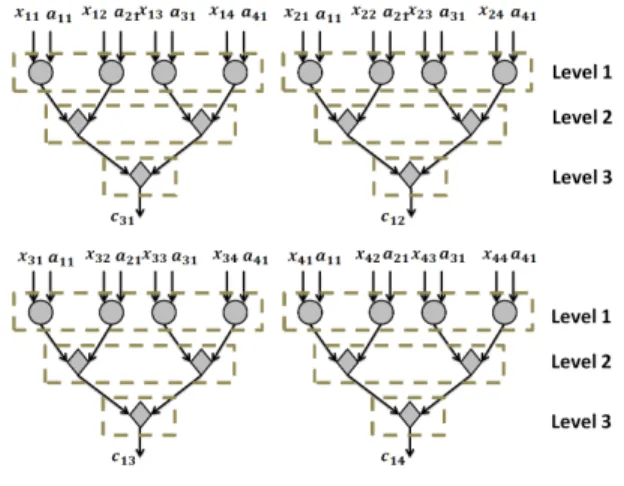
additions andnadditions to compute final vectory. In our DAG analysis we consider vector multiplication since matrix-vector multiplication is compute intensive part of the routine and it is essential to exploit parallelism in matrix-vector multiplication to accelerate DGEMV routine. DAGs for matrix-vector multipli-cation are shown in in the figure 5.
It can be observed from DAGs of matrix-vector multiplication that all the multiplication in matrix-vector multiplication can be executed in parallel and matrix-vector multiplication can be realized as series ofddotroutine calls.
4.3 Matrix-matrix Operations (Level-3 BLAS)
Here we first review some of the matrix multiplication algorithms and present graph based analysis of these algorithms. We briefly discuss parallelism in different matrix multiplication algorithms. Based on the analysis, we choose matrix multiplication algorithm. In the following subsection of the paper, we present design of a PE that can efficiently exploit ILP in the chosen matrix multiplication algorithm.
4.3.1 Matrix Multiplication Algorithms
Over the years there have been several matrix multiplication algorithms proposed in the literature. In this subsection, we review and analyze Strassen’s Matrix Multiplication (SMM), Winograd’s Matrix Multiplication (WMM), and General Matrix
Multiplication (GEMM). We consider A =
A11 A12 A21 A22 , and B= B11 B12 B21 B22
as input matrices andC=
C11 C12
C21 C22
as output matrix whereA, B, C are equal sized block matrices and
A, B, C∈R2n× R2n.
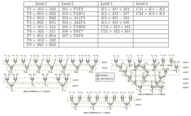
4.3.2 Strassen’s Matrix Multiplication
SMM algorithm is described in table 2 for2×2block matrix. Typically, SMM has two steps, 1) decompose step, and 2) merge step. In decompose step, matrix is divided in block matrices andM1 to M7 are computed. In merge step, C11 toC22 are computed. Directed Acyclic Graphs (DAGs) for SMM are shown in figure 6 forn = 1. It can be observed in the DAGs of SMM that the computation ofC11toC22depends on computations of
M1toM7.
This dependencies in the DAGs of SMM results in higher execution time of SMM. It can also be observed from DAGs of SMM in figure 6 that M1 to M7 can potentially be executed in parallel and C11 to C22 can also be executed in parallel. One of the way this parallelism can be exploited is through processor pipeline and pipelined arithmetic units. Asymptotic complexity of SMM isO(n2.81).
4.3.3 Winograd’s Matrix Multiplication
WMM algorithm operates on the same principle as SMM as shown below:
It can be observed from WMM algorithm that it takes7block matrix multiplications and15matrix additions unlike SMM where the number of block matrix multiplication is same but the number of matrix additions are18. DAGs for WMM are shown in figure 6 forn= 1.
WMM has same asymptotic complexity as SMM. In practical scenarios, execution time of WMM is observed to be slightly less than SMM due to fewer additions.
4.3.4 General Matrix Multiplication
GEMM for multiplication of A and B can be described by
following expressions:
C11 =A11B11 +A12B21
C12 =A11B12 +A12B22
C21 =A21B11 +A22B21
TABLE 2: Computations in the different Levels of DAGs of SMM at first step of Recursion in2×2Block Matrix Multiplication
Level 1 Level 2 Level 3 Level 4
T1 =A11 +A22 M1 =T1T2 K1 =M1 +M4 C11 =K1−K2 T2 =B11 +B22 M2 =T2B11 K2 =M3−M7 C22 =K3 +K4 T3 =B12−B22 M3 =A11T3 K3 =M1−M2 T4 =B21−B11 M4 =A22T4 K4 =M3 +M6 T5 =A11 +A12 M5 =T5B22 C12 =M3 +M5 T6 =A21−A11 M6 =T6T7 C21 =M2 +M4 T7 =B11 +B12 M7 =T8T9 T8 =A12−A22 T9 =B21 +B22
Fig. 6: SMM, WMM, and GEMM for2×2Block Matrix
TABLE 3: Computations in the different Levels of DAGs of WMM at first step of Recursion in2×2Block Matrix Multiplication
Level 1 Level 2 Level 3 Level 4 Level 5 Level 6
S1 =A21 +A22 S2 =S1−A11 S4 =A12−S2 M6 =S4B22 V2 =V1 +M4 C12 =V1 +K1 S3 =A11−A21 S6 =B22−S5 S8 =S6−B21 M7 =A22S8 K1 =M5 +M6 C21 =V2−M7 S5 =B12−B11 M4 =S3S7 M1 =S2S6 V1 =M1 +M2 C22 =V2 +M5 S7 =B22−B12 M5 =S1S5 M2 =A11B11 C11 =M2 +M3 M3 =A12B21
DAGs for a2×2matrix is shown in figure 6. It can be observed from the DAGs of GEMM that it takes 8 multiplications and 4
additions. Asymptotic complexity of GEMM isO(n3).
SMM and WMM have lower asymptotic complexities com-pared to GEMM. A major disadvantage of SMM and WMM is that they are more suitable for square matrices where size is a power of two. For the matrix sizes where this condition is not met, a complex matrix partitioning scheme is required. Hence, we adopt GEMM over SMM and WMM due to following reasons:
• A complex partitioning scheme required for the matrices in SMM and WMM results in a intricate scheduling scheme for the blocks of input matrices. A way to alleviate these complications is to zero pad the matrices. This zero
padding results in few more computations, mostlyO(n2).
Thezeropadding does not reduce the complexity of the implementation since naivezero padding scheme is not efficient
• GEMM has higher pedagogical importance than SMM
and WMM. GEMM is highly preferred to evaluate the emerging architectures over SMM and WMM due to its simple structure and ease of implementation
4.3.5 Anatomy of General Matrix Multiplication
To discuss available parallelism in GEMM, we take a matrix multiplication of size4×4as an example.
Fig. 7: DAGs in GEMM for4×4Matrix
DAGs form=n= 4for algorithm 1 are shown in figure 7 for computation of elementsc11toc44. It can be observed in the figure 7 that all the multiplications in the block of the matrix can be computed in parallel. The dependencies are due to accumulation of the multiplied elements of the input matrices.
Fig. 8: PE Architecture
Potentially, in multiplication of matrix of sizen×n, all then3
multiplications can be computed in parallel. In case of4×4matrix, all 16elements can be computed in parallel as shown in figure 7. The accumulation process while computing the elements of the resultant matrix enforce the dependencies resulting in pipeline stalls. These pipeline stalls can be avoided by computing multiple elements in parallel-pipeline manner.
Algorithm 3Block General Matrix Multiplication
1: Allocate memories for input and output matrices
2: fori= 1tom/4do 3: forj = 1ton/4do 4: fork= 1ton/4do 5: C = BLOCK4ADD(BLOCK4MUL(A,B),C) 6: end for 7: end for 8: end for
Algorithm 3 depicts DGEMM with4×4block matrix multi-plication (assuming that the matrix dimensions are multiple of4). In algorithm 3, BLOCK4MUL is multiplication of matrices of size
4×4, and BLOCK4ADD is addition of matrices of size4×4. A pitfall in the unrolling scheme is the exigency of locally available registers. Typically, forn×nmatrix, if fully unrolled, requires
3n2 registers. Hence, for a large matrix, it can not be unrolled
due to lack of locally available registers, but a small block of the matrix can be unrolled to exploit the fine grained parallelism in the block through processor pipeline and pipelined arithmetic units. In parallel realization of GEMM, different blocks of4×4 can be computed in parallel on different PEs. While realizing GEMM on a single PE, we try to exploit parallelism that is available in a block of4×4 and in parallel realization on REDEFINE, we try to exploit parallelism across the blocks.
In the next section we present a PE design to skillfully exploit the parallelism that exist in the block of4×4matrix.
4.4 Processing Element Design
For initial design of PE, we consider classical sequential archi-tecture model. As a first design, we take a fully pipelined double precision floating point adder, and multiplier arithmetic units as compute resources. Architecture of PE is shown in figure 8.
As shown in the figure 8, the initial design of PE consists of an Instruction Memory, a Decoder to decode the instructions,
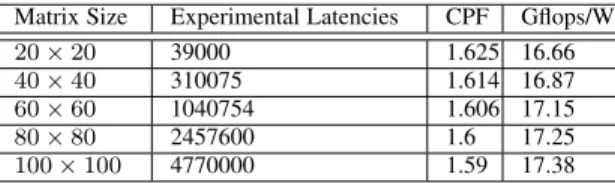
TABLE 4: Latencies, CPF and Efficiency
Matrix Size Experimental Latencies CPF Gflops/W
20×20 39000 1.625 16.66
40×40 310075 1.614 16.87
60×60 1040754 1.606 17.15
80×80 2457600 1.6 17.25
100×100 4770000 1.59 17.38
a Register File with64registers, and pipelined double precision Floating Point Unit (FPU) [34][35]. The FPU consists of a multi-plier, an adder, a square root, and a divider. For computing matrix multiplication with large matrices, we choose 4×4 as a block matrix. For the matrices that are not multiple of4, we partition them in the blocks of4×4as many times as possible and for the residual matrix, we perform unblocked multiplication. Operation of the PE can be described in the following steps:
• Step 1:Bring the input matrices to the Register File that by sending Load request to the upper level of the memory
• Step 2:Perform matrix multiplication
• Step 3:Store back the resultant matrix to the upper level of memory
4.5 Simulation Environment and Initial Results
For simulations we connect PE shown in the figure 8 to exter-nal/global memory. Initially we use 64 (64−bitwide) registers, 16KB of instruction memory for our experiments. We model global/external memory delay by placing pipelined delay of 20
stages.
4.5.1 Initial Results
For our experiments, we choose matrix sizes20×20,40×40,
60×60,80×80, and100×100as a representative matrix sizes for our experiments.
It can be observed in the table 4 that as we increase the matrix size, the CPF decreases and saturates around 1.6 while performance in terms of Gflops/watt is observed to be at 17.3 Gflops/watt at 0.2 GHz. In other words, as we increase the matrix size, the FPC saturates at 62.5% of peak floating point operations per cycle. Here, since, we can potentially compute one multiplication and one addition in parallel, the peak FPC = 2.
In this section, we reviewed some of the matrix multiplication techniques. We discussed asymptotic complexity and graph based analysis of three different matrix multiplication algorithms. We justified our choice of GEMM over SMM and WMM algorithms. We presented additional details of GEMM with an example of
4×4matrix and proposed an initial design of a PE that achieves CPF of 1.6 and performance of 17.3 Gflops/watt. Intuitively, performance of the PE can be improved methodically by enriching the PE with compute and memory resources.
5
M
ICRO-
ARCHITECTURALE
NHANCEMENTS INPE
ANDP
ARALLELR
EALIZATION ONREDEFINE
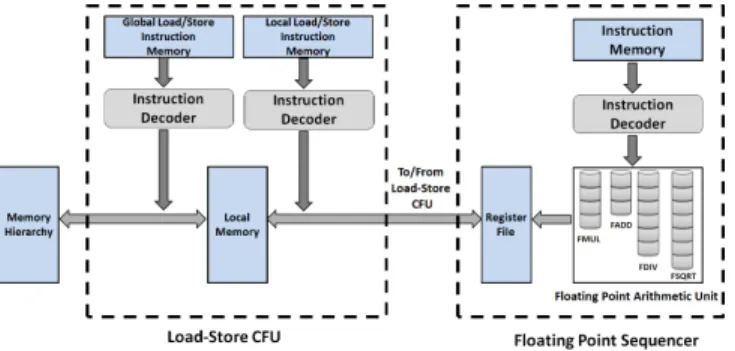
Based on anatomy of the GEMM and design of the PE presented in section 4.4, in this section we dwell on micro-architectural en-hancements of the PE. We methodically enhance PE that improves CPF. The PE described in section 4.4 is considered as a Floating Point Sequencer in this section.
Fig. 9: PE with FPS and Load-Store CFU
5.1 Introducing Local Memory and Load-Store CFU
Major drawbacks of the PE design presented in section 4.4 are no overlap of computations and communication and lack of exploitation of data locality in GEMM. To address these issues, we introduce a Load-Store CFU that operates simultaneously with FPS (depending on availability of data), and facilitates overlap of computation and communication. We also place a Local Memory (LM) of size256kbin the Load-Store CFU to exploit data locality in GEMM. Enhanced PE design with FPS and Load-Store CFU is shown in figure 9.
Introduction of an LM in Load-Store CFU inside PE improves the data locality. This improved data locality creates further opportunities for exploitation of higher ILP by increasing compute resources in FPS. Increased compute resources in the FPS demand for improvisation in the data availability in the Register File for computations. In this section we present methodical architectural enhancements in the PE for reduction in latency4 in execution
of GEMM. These enhancements in the PE ensures lower latency in execution of GEMM leading to overlap between computation and communication up-to 90% in GEMM and we are also able to achieve up-to 74% of the peak CPF5. To highlight the reduction
in the latency due to each architectural enhancement, we consider
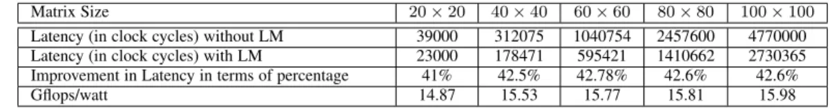
20×20,40×40,60×60,80×80, and100×100matrix sizes as a representative for our experiments. Reduction in the latency due to introduction of Load-Store CFU and LM (refer figure 9) is shown in the table 5.
It can be observed in the table 5 that introduction of LM in the Load-Store CFU improves performance by 2x and as we increase matrix size the performance improves due to improved data locality.
5.2 Special Instructions
In the first enhancement, we try to exploit higher ILP by increasing resources in the FPS that in turn improves performance signifi-cantly. This improved performance motivates us to improve data availability in the Register File residing inside FPS. We introduce two types of special instruction: 1) DOT instructions that are ex-ecuted in FPS on a specialized fully pipelined hardware structure, and 2) Block Data Load and Block Data Store instructions that are executed in the Load-Store CFU.
5.2.1 DOT Instruction
Since we support block size of 4 ×4, we introduce a hard-ware that can perform inner product of a4-element vector. The
4. Latency in terms of clock cycles
5. Peak CPF =N umber of Arithmetic U nits that can f unction concurrently1
Fig. 10: RDP of DOT Instruction and different data-path derived by different configurations of DOT
hardware structure to compute 4-element vector inner product is shown in figure 10. We further make this hardware structure reconfigurable to support 2-element and 3-element vector inner products to support different matrix sizes. We name this unit as a Reconfigurable Data-path (RDP). Through reconfiguration, RDP can be re-casted to perform macro operations encountered in some of the algorithms in BLAS discussed in the section 4. The RDP is shown in figure 10.
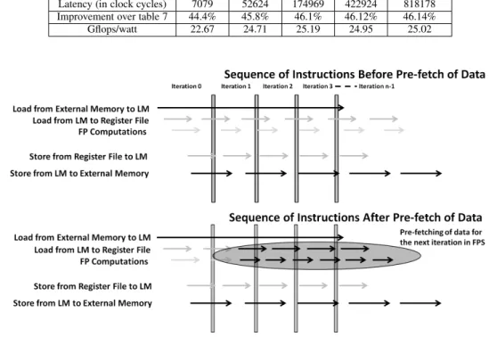
For larger matrices (> 4×4) that do not fit in the Register File in FPS for matrix multiplication, we use block size of4×4. For the matrices that do not have their size as multiple of 4, we use 2-element, and 3-element inner product configurations of RDP. In this exposition, we restrict our experiment to the matrices with size of multiple of4 and hence we use4-element inner product configuration (also termed as DOT4 configuration) of RDP. DOT4 configuration of RDP has a15-stage deep pipeline. Assuming no pipeline stalls, we can potentially maintain15DOT4 instructions in a state of execution. This DOT4 instruction leads to exploitations of higher ILP in a block of 4×4 in GEMM. Improvement in latency of GEMM due to DOT4 instruction is shown in table 6.
It can be observed from the table 6 that as we increase the matrix size, the benefit due to DOT instruction improves. This is due to improved exploitation of ILP in the FPS.
5.2.2 Block Data Load and Block Data Store Instructions
We further aim to reduce handshaking between LM and GM. This reduction in the handshaking in-turn improves data availability in the Register File. In order to reduce the handshaking between PE and the next level of the Memory, we introduce instructions that can load/store data in a block fashion. Performance improvement due to Block Data Load and Block Data Store is shown in table 7 where we have used4×4as a block size for the transfer.
It can be observed from the table 7 that as we increase matrix size, the benefit due to Block Data Load/Store does not improve. Rather the performance is observed to be saturating. This is because of the constant block size of4×4across all the matrix sizes. Supporting larger block size is not possible due to limited registers availability in the Register File in the FPS. It can also be observed in table 7 that the latency gap between20×20and
40×40, and40×40and60×60is also decreasing and it is likely to saturate at some point. Further experiments show that the gap saturates at10%for larger matrix sizes.
TABLE 5: Latencies of20×20,40×40,60×60,80×80, and100×100GEMM (with LM and Load-Store CFU (PE-Architectural Enhancement1(AE1))
Matrix Size 20×20 40×40 60×60 80×80 100×100
Latency (in clock cycles) without LM 39000 312075 1040754 2457600 4770000
Latency (in clock cycles) with LM 23000 178471 595421 1410662 2730365
Improvement in Latency in terms of percentage 41% 42.5% 42.78% 42.6% 42.6%
Gflops/watt 14.87 15.53 15.77 15.81 15.98
TABLE 6: Latencies of20×20,40×40,60×60,80×80, and100×100GEMM (PE with Load-Store CFU, with DOT instruction (PE-Architectural Enhancement2(AE2))
Matrix Size 20×20 40×40 60×60 80×80 100×100
Latency (in clock cycles) 15251 113114 371699 877124 1696921
Improvement over table 5 33.7% 36.6% 37.57% 37.82% 37.85%
Gflops/watt 10.52 11.49 11.85 11.93 12.06
TABLE 7: Latencies of20×20,40×40,60×60,80×80, and100×100GEMM (PE with Load-Store CFU, with DOT4, and Block Data Load/Store instructions (PE-Architectural Enhancement3(AE3))
Matrix Size 20×20 40×40 60×60 80×80 100×100
Latency (in clock cycles) 12745 97136 324997 784838 1519083
Improvement over table 6 16.4% 14.1% 12.5% 10.51% 10.48%
Gflops/watt 12.59 13.38 13.56 13.33 13.47
5.3 Bandwidth Increase
Increased resources in the FPS improves performance by almost
2x, and reduced handshaking between LM and the upper level of the memory improves performance by 10%. We still see significant gap between our desired performance and attained performance. The reason for this gap is mainly because of under utilization of the RDP that is configured as DOT4. In order to improve resource utilization of RDP, in this architectural enhancement,
we increase bandwidth between FPS and Load-Store CFU to 4
times. We consider increase in the bandwidth to4times since the block size supported in FPS is4×4. We transfer256-bits between FPS and Load-Store CFU in contrast to previous realization where we transfered64-bit data. The communication between FPS and Load-Store CFU at higher rate ensures better data availability in the Register File of FPS. The performance improvement due to increase in the bandwidth is shown in table 8.
It can be observed in table 8 that as we increase the matrix size the benefits due to increased bandwidth between FPS and Load-Store CFU in the PE improves. This is mainly because of better utilization of RDP (here configured as DOT4).
5.4 Pre-fetching
To improve the utilization of RDP further in the FPS, we restruc-ture the loop in GEMM. We re-write algorithm 1 as algorithm 4.
Algorithm 4General Matrix Multiplication with Pre-fetching
1: Allocate memories for input and output matrices
2: fori= 1tomdo 3: forj = 1tondo 4: C[i][j] =A[i][k]×B[k][j] 5: fork= 1tondo 6: C[i][j] =A[i][k]×B[k][j] +C[i][j] 7: end for 8: end for 9: end for
Re-structuring the loops in the algorithm allows us to pre-fetch the matrix block required for the next iteration. This results in better exploitation of FPU pipeline by reduced instruction stalls in FPS as shown in figure 11. The shaded portion in the figure 11 depicts the reduction in the instruction stalls in FPS when there is a pre-fetch of the block of the matrix required in the next iteration for computation. In figure 11, there are two portions, 1) before pre-fetching, and 2) after pre-fetching. Arrows in the figures depict execution of different types of operations such as computations in FPS, loading/storing of data from/to GM (or EM) memory, loading/storing of data from/to GM.
Improvement attained by pre-fetching is shown in table 9. It can be observed in the table 9 that as we increase matrix size the benefits due to pre-fetching increases. This is mainly because of improvement in data availability in the Register File of the FPS.
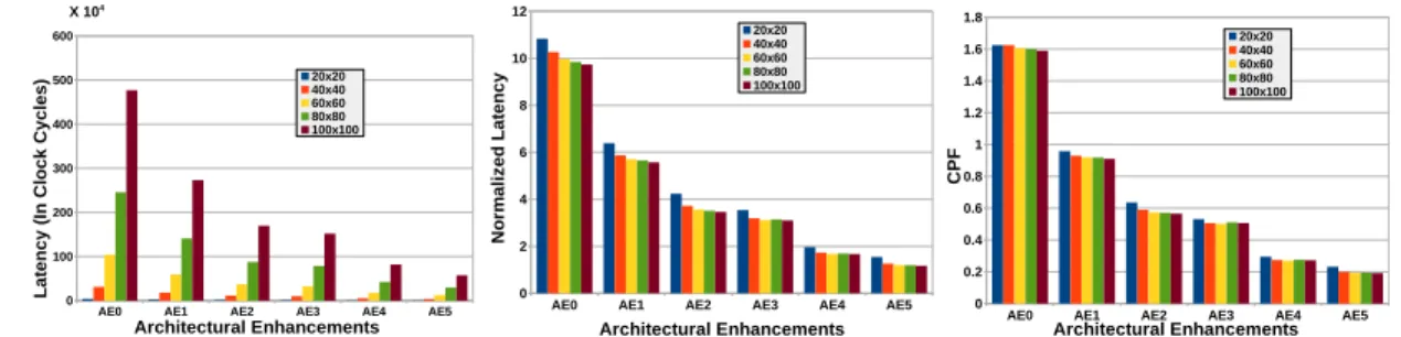
Collectively, the reduction in execution cycles of GEMM can be seen in the figure 12(a) as we perform different architectural enhancements in the PE. It can be clearly observed that finally we get speed-up of 7x for matrix of size20×20, 8.13x for the matrix of size40×40, and 8.34x for the matrix of size60×60[36].
It can be observed from figure 12(b) that as we perform different architectural enhancements, the ratio of Latency to computations reduces. If we denote the ratio of Latency to total computations byαthen
α= Latency
T otal Computations in T erms of DOT4 (7)
It can be observed in the figure 12(b) that as we increase matrix sizeαasymptotically approaches1.α= 1is a case where there is a complete overlap of computation and communication. Complete overlap of computations and communication is not possible in the real life scenario and henceαcan never become1.
Figure 12(c) depicts CPF for matrices of size20×20,40×40, and60×60. It can be observed in the figure 12(c) that as we perform enhancements the CPF tends to decrease and this trend is observed across all the matrices. Figure 12(d) depicts FPC (where
TABLE 8: Latencies of20×20,40×40,60×60,80×80, and100×100GEMM (PE with Load-Store CFU, with DOT and Block Data Load/Store instructions, increased bandwidth (PE-Architectural Enhancement4(AE4))
Matrix Size 20×20 40×40 60×60 80×80 100×100
Latency (in clock cycles) 7079 52624 174969 422924 818178
Improvement over table 7 44.4% 45.8% 46.1% 46.12% 46.14%
Gflops/watt 22.67 24.71 25.19 24.95 25.02
Fig. 11: Pre-fetching Matrix Elements for the Next Iteration
TABLE 9: Latencies of20×20,40×40,60×60,80×80, and100×100GEMM (PE with Load-Store CFU, with DOT and Block Data Load/Store instructions, increased bandwidth and data pre-fetching (PE-Architectural Enhancement5(AE5))
Matrix Size 20×20 40×40 60×60 80×80 100×100
Latency (in clock cycles) 5561 38376 124741 298161 573442
Improvement over table 8 21.44% 27.07% 28.70% 29.5% 29.9%
Gflops/watt 28.86 33.88 35.33 35.11 35.70
FPC = 1/CPF). It can be observed from figure 12(d) that, as we perform enhancements in the PE, FPC improves dramatically. Although CPF and FPC are good measure of performance of a PE, they do not convey enough information about how efficiently compute resources are utilized in the PE.
Percentage of peak FPC attained in PE after every enhance-ment is shown in figure 12(e). Figure 12(e) depicts an interesting trend where the peak FPC reduces drastically and then with fur-ther architectural enhancements, improves. As our enhancements suggests, in the first enhancement where we place Load-Store CFU with LM for overlap of computation and communication, the FPC achieved saturates at 54% of the peak FPC6. We strongly intend to break this saturation point since 54% of the peak is not a satisfactory performance. In order to break this saturation point we further enhance FPS with compute resources that leads to higher theoretical peak FPC7. At this point achieved FPC reduces atAE2as shown in the figure 12(e). This is because of increased compute resources. Our further enhancements help us to improve the resource utilization of the increased resources in FPS and achieve up-to 74% of the peak FPC of the PE.
We presented methodical architectural enhancements to
im-6. Here peak FPC =CP F1 = 11
2 = 2
7. Here peak FPC =CP F1 = 11
7
= 7. Increase in peak FPC is due to DOT4
instruction
prove the performance of PE. Through architectural customiza-tions, we could break saturation point at 54% and improve perfor-mance of PE. In other words, we showed that the perforperfor-mance of the algorithms can be improved by customizations that are specific to the algorithms. Here, we showed this with example of GEMM which is a Level-3 BLAS. Finally, 35.7 Gflops/watt in the PE is achieved through carefull realization of Level-3 BLAS.
5.5 Parallel Realization of Level-3 BLAS
For parallel realization of DGEMM, our two different simulation environments are shown in figure 12(k). In figure 12(k), shaded portion of the Tile array (except the last column) which is 2x2
is used for the computations where we realize DGEMM while the last column is used for storing input and output matrices. We use Octave for generating input matrices. Similarly, we use3×3
portion of the Tile array for realizing DGEMM.
In our experiments, if output matrix is of sizen×nthen we divide the output matrix into blocks of nb ×n
b whereb×bis the Tile array that we are using. In our experimentsb = 2or3. For example, if output matrix is of size 20×20, and we are using
2×2of the Tile array to compute the DGEMM, we divide output matrices into10×10block matrices. Now, in each Tile that we are using, we compute one of the block of size10×10. Similarly, if output matrix is of size60×60, and Tile array that is used for
AE0 AE1 AE2 AE3 AE4 AE5 0 100 200 300 400 500 600 20x20 40x40 60x60 80x80 100x100 Architectural Enhancements L a te n c y ( In C lo c k C y c le s ) X 104
(a) Reduction in the Latency in DGEMM Due to Architecture Enhancements
AE0 AE1 AE2 AE3 AE4 AE5
0 2 4 6 8 10 12 20x20 40x40 60x60 80x80 100x100 Architectural Enhancements N o rm a li ze d L a te n c y
(b) Latencies Normalized to Total Com-putations in terms of DOT4 in DGEMM
AE0 AE1 AE2 AE3 AE4 AE5
0 0.2 0.4 0.6 0.8 1 1.2 1.4 1.6 1.8 20x20 40x40 60x60 80x80 100x100 Architectural Enhancements C P F
(c) Cycles per Floating Point Operation in DGEMM
AE0 AE1 AE2 AE3 AE4 AE5
0 1 2 3 4 5 6 20x20 40x40 60x60 80x80 100x100 Architectural Enhancements F P C
(d) Floating Point Operations per Cycle in DGEMM
AE0 AE1 AE2 AE3 AE4 AE5
0 10 20 30 40 50 60 70 80 20x20 40x40 60x60 80x80 100x100 Architectural Enhancements P e rc e n ta g e
(e) Percentage of Peak FPC in DGEMM with Each Architectural Enhancement
AE0 AE1 AE2 AE3 AE4 AE5
0 5 10 15 20 25 30 35 40 45 20x20 40x40 60x60 80x80 100x100 Architectural Enhancements P e rc e n ta g e
(f) Percentage of Peak FPC in DGEMV with Each Architectural Enhancement
AE0 AE1 AE2 AE3 AE4 AE5
0 2 4 6 8 10 12 20 40 60 80 100 Architectural Enhancements P e rc e n ta g e
(g) Percentage of Peak FPC in DDOT with Each Architectural Enhancement
AE0AE1AE2AE3AE4AE5 AE0AE1AE2AE3AE4AE5 AE0AE1AE2AE3AE4AE5 AE0AE1AE2AE3AE4AE5 0 5 10 15 20 25 30 35 40 20x20 40x40 60x60 80x80 100x100 Architectural Enhancements G fl o p s /w a tt 0.2 GHz 0.33 GHz 0.95 GHz 1.81 GHz
(h) Gflops/watt for DGEMM at 0.2GHz, 0.33GHz, 0.95GHz, and 1.81GHz AE0AE1AE2AE3AE4AE5 AE0AE1AE2AE3AE4AE5 AE0AE1AE2AE3AE4AE5 AE0AE1AE2AE3AE4AE5 0 1 2 3 4 5 6 7 20x20 40x40 60x60 80x80 100x100 Architectural Enhancements G fl o p s /m m ^ 2 0.2 GHz 0.33 GHz 0.95 GHz 1.81 GHz
(i) Gflops/mm2for DGEMM at 0.2GHz,
0.33GHz, 0.95GHz, and 1.81GHz Intel C ore Nvid ia G TX48 0 SM Alte ra S tratix IV Clea rSpe ed C SX70 0 Intel C ore i7 H assw ell Nvid ia Tes la C 2050 0 20 40 60 80 100 120 140 160 Platforms P er fo rm an ce Im p ro ve m en t In -t er m s o f G fl o p s/ w at t (j) Performance Comparison of
REDEFINE-PE with Other Platforms
(k) Simulation Environment where Tile array of2×2is used
for realizing DGEMM
computing DGEMM is of size3×3 then block of 20×20is computed in each of the Tile of REDEFINE.
0 2 4 6 8 10 12 14 16 2x2 3x3 4x4 Matrix Size S p e e d -u p
Fig. 13: Speed-up in REDEFINE for DGEMM for Different Configurations
Speed-up attained in REDEFINE is is shown in the figure 13 when Tile array of size2×2,3×3, and4×4are used for the experiments. It can be observed from the figure 13 that when we use Tile array of2×2the speed-up over PE realization approaches
4as we increase matrix size. When we use Tile array of3×3the speed-up over PE realization approaches9, and for Tile array of size4×4the speed-up attained approaches 16. For small matrices, communication with the last column of the Tile array is dominant over computations in the Tile. For example, for a matrix of size
20×20and Tile array size of2×2, each Tile computes10×10
block of the resultant matrix. Ignoring the coefficient of the highest order term, there will be103computations over102loads/stores. Computation to communication ratio in for20×20matrix will be
10in each Tile. For matrix a of size60×60where each Tile will compute a block of20×20matrix, computation to communication ratio is20.
One more observation we make here is that, as we increase the matrix size, speed-up in REDEFINE over PE saturates. This is because of the saturation in the parallelism exploited by the PE that is attached in each Tile of REDEFINE.
5.6 Discussion on Results
In this section, we results for the PE that we presented in section 4.4. We use the estimation methodology presented in [20], [21], and [22] for fair comparison of the architecture. Since, NoC used in REDEFINE, we restrict our evaluation and comparison to PE level. As shown in the figure 12(j), it can be observed that the performance of the PE is 40-140x better than Intel Core architectures while 7-139x better than Nvidia GPUs. Compared to Altera FPGA, PE is 10x better in terms of Gflops/watt while compared to ClearSpeed CSX700 it is almost 3x better.
6
C
ONCLUSIONWhile the recent realizations for matrix computations focus on architectural customization for DLA, in this paper we presented a novel way of algorithm-architecture co-design for breaking the performance saturation point in Level-3 BLAS and exploiting underlying compute and memory resources more efficiently. In algorithm-architecture co-design, we first realized Level-3 BLAS on off-the-shelf processors and exhibited that the performance achieved by these off-the-shelf processors in DGEMM is not satisfactory. The performance in the off-the-shelf Intel and AMD
processors saturates at 15-17% at 65W with the best program-ming efforts. This dis-satisfactory performance is mainly due to inefficiently exploited compute and memory resources of the underlying platform. We could sense a scope here in breaking this saturation point in a custom architecture and performed analysis of Level-1, Level-2, and Level-3 BLAS, and designed a PE that could efficiently execute BLAS routines. We further enhanced this PE with several features such that we could efficiently exploit compute resources and memory resources in the PE and achieve performance of 35.7 Gflops/watt that is much higher than the off-the-shelf processors and GPUs. We attached this PE in REDE-FINE for parallel realization of BLAS and showed that the speed-up achieved in the parallel realization is commensurate with the number of Tiles used and hence we showed that our solution is scalable.
R
EFERENCES[1] E. Anderson, Z. Bai, C. Bischof, S. Blackford, J. Demmel, J.
Don-garra, J. Du Croz, A. Greenbaum, S. Hammarling, A. McKenney, and
D. Sorensen,LAPACK Users’ Guide, 3rd ed. Philadelphia, PA: Society
for Industrial and Applied Mathematics, 1999.
[2] E. Anderson, Z. Bai, J. Dongarra, A. Greenbaum, A. McKenney,
J. Du Croz, S. Hammerling, J. Demmel, C. Bischof, and D. Sorensen, “Lapack: A portable linear algebra library for high-performance
computers,” in Proceedings of the 1990 ACM/IEEE Conference on
Supercomputing, ser. Supercomputing ’90. Los Alamitos, CA, USA:
IEEE Computer Society Press, 1990, pp. 2–11. [Online]. Available: http://dl.acm.org/citation.cfm?id=110382.110385
[3] J. Kurzak, P. Luszczek, A. YarKhan, M. Faverge, J. Langou,
H. Bouwmeester, and J. Dongarra, “Multithreading in the plasma library,” 2013.
[4] B. J. Smith, “R package magma: Matrix algebra on gpu and multicore
architectures, version 0.2.2,” September 3, 2010, [On-line] http://cran.r-project.org/package=magma.
[5] J. York and D. Chiou, “On the asymptotic costs of multiplexer-based
reconfigurability,” inThe 49th Annual Design Automation Conference
2012, DAC ’12, San Francisco, CA, USA, June 3-7, 2012, 2012, pp. 790– 795. [Online]. Available: http://doi.acm.org/10.1145/2228360.2228503
[6] G. Ansaloni, P. Bonzini, and L. Pozzi, “Egra: A coarse grained
recon-figurable architectural template,”Very Large Scale Integration (VLSI)
Systems, IEEE Transactions on, vol. 19, no. 6, pp. 1062–1074, June 2011.
[7] A. Fell, P. Biswas, J. Chetia, S. K. Nandy, and R. Narayan, “Generic
routing rules and a scalable access enhancement for the network-on-chip
reconnect,” inSoCC, 2009, pp. 251–254.
[8] J. Nimmy, C. R. Reddy, K. Varadarajan, M. Alle, A. Fell, S. K. Nandy,
and R. Narayan, “Reconnect: A noc for polymorphic asics using a low
overhead single cycle router,” inASAP, 2008, pp. 251–256.
[9] J. Dongarra, “The linpack benchmark: An explanation,” inProceedings
of the 1st International Conference on Supercomputing. London,
UK, UK: Springer-Verlag, 1988, pp. 456–474. [Online]. Available: http://dl.acm.org/citation.cfm?id=647970.742568
[10] A. YarKhan, J. Kurzak, and J. Dongarra, “Quark users’ guide: Queueing and runtime for kernels,” Innovative Computing Laboratory, University of Tennessee, Tech. Rep., 2011.
[11] F. G. Van Zee,libflame: The Complete Reference. lulu.com,
2009.
[12] P. Bientinesi, J. Gunnels, M. Myers, E. Quintana-Ort, T. Rhodes, R. van de Geijn, and F. Van Zee, “Deriving dense linear algebra
libraries,”Formal Aspects of Computing, vol. 25, no. 6, pp. 933–945,
2013. [Online]. Available: http://dx.doi.org/10.1007/s00165-011-0221-4 [13] R. C. Whaley and A. Petitet, “Minimizing development and maintenance
costs in supporting persistently optimized BLAS,” Software: Practice
and Experience, vol. 35, no. 2, pp. 101–121, February 2005,
http://www.cs.utsa.edu/˜whaley/papers/spercw04.ps. [14] R. C. Whaley, A. Petitet, and J. J. Dongarra, “Automated empirical
optimization of software and the ATLAS project,” Parallel
Comput-ing, vol. 27, no. 1–2, pp. 3–35, 2001, also available as University of Tennessee LAPACK Working Note #147, UT-CS-00-448, 2000 (www.netlib.org/lapack/lawns/lawn147.ps).
[15] Q. Wang, X. Zhang, Y. Zhang, and Q. Yi, “Augem: Automatically generate high performance dense linear algebra kernels on x86 cpus,”
in Proceedings of the International Conference on High Performance
Computing, Networking, Storage and Analysis, ser. SC ’13. New
York, NY, USA: ACM, 2013, pp. 25:1–25:12. [Online]. Available: http://doi.acm.org/10.1145/2503210.2503219
[16] Z. Xianyi, W. Qian, and Z. Yunquan, “Model-driven level 3 blas
performance optimization on loongson 3a processor,” inParallel and
Distributed Systems (ICPADS), 2012 IEEE 18th International Conference on, Dec 2012, pp. 684–691.
[17] L. Wang, W. Wu, Z. Xu, J. Xiao, and Y. Yang, “BLASX: A high performance level-3 BLAS library for heterogeneous multi-gpu
computing,” in Proceedings of the 2016 International Conference on
Supercomputing, ICS 2016, Istanbul, Turkey, June 1-3, 2016, 2016, pp. 20:1–20:11. [Online]. Available: http://doi.acm.org/10.1145/2925426. 2926256
[18] L. Djinevski, S. Ristov, and M. Gusev, “Superlinear speedup for matrix
multiplication in gpu devices,” inICT Innovations 2012. Springer Berlin
Heidelberg, 2013, pp. 285–294.
[19] F. Merchant, T. Vatwani, A. Chattopadhyay, S. Raha, S. K. Nandy, and R. Narayan, “Achieving efficient qr factorization by
algorithm-architecture co-design of householder transformation,” in29th
Interna-tional Conference on VLSI Design, VLSID 2016, Kolkata, India, January 4-8, 2016.
[20] A. Pedram, S. Z. Gilani, N. S. Kim, R. A. van de Geijn, M. J. Schulte, and A. Gerstlauer, “A linear algebra core design for efficient level-3 blas,” in ASAP, 2012, pp. 149–152.
[21] A. Pedram, R. A. van de Geijn, and A. Gerstlauer, “Codesign tradeoffs
for high-performance, low-power linear algebra architectures,” IEEE
Trans. Computers, vol. 61, no. 12, pp. 1724–1736, 2012. [Online]. Available: http://doi.ieeecomputersociety.org/10.1109/TC.2012.132 [22] A. Pedram, A. Gerstlauer, and R. A. van de Geijn, “Algorithm,
architecture, and floating-point unit codesign of a matrix factorization
accelerator,”IEEE Trans. Computers, vol. 63, no. 8, pp. 1854–1867,
2014. [Online]. Available: http://dx.doi.org/10.1109/TC.2014.2315627 [23] T. Chen, R. Raghavan, J. Dale, and E. Iwata, “Cell broadband engine
architecture and its first implementation x2014;a performance view,”IBM
Journal of Research and Development, vol. 51, no. 5, pp. 559–572, Sept 2007.
[24] S. Williams, J. Shalf, L. Oliker, S. Kamil, P. Husbands, and K. Yelick,
“Scientific computing kernels on the cell processor,” Int. J. Parallel
Program., vol. 35, no. 3, pp. 263–298, Jun. 2007. [Online]. Available: http://dx.doi.org/10.1017/s10766-007-0034-5
[25] Y. Nishikawa, M. Koibuchi, M. Yoshimi, A. Shitara, K. Miura, and H. Amano, “Performance analysis of clearspeed’s CSX600
interconnects,” in IEEE International Symposium on Parallel and
Distributed Processing with Applications, ISPA 2009, Chengdu, Sichuan, China, 10-12 August 2009, 2009, pp. 203–210. [Online]. Available: http://doi.ieeecomputersociety.org/10.1109/ISPA.2009.102
[26] Y. Nishikawa, M. Koibuchi, M. Yoshimi, K. Miura, and H. Amano, “Performance improvement methodology for clearspeed’s CSX600,” in 2007 International Conference on Parallel Processing (ICPP 2007), September 10-14, 2007, Xi-An, China, 2007, p. 77. [Online]. Available: http://dx.doi.org/10.1109/ICPP.2007.66
[27] J. Gonzalez and R. C. Nez, “Lapackrc: Fast linear algebra
kernels/solvers for fpga accelerators,”Journal of Physics: Conference
Series, vol. 180, no. 1, p. 012042, 2009. [Online]. Available: http://stacks.iop.org/1742-6596/180/i=1/a=012042
[28] Y.-G. Tai, C.-T. D. Lo, and K. Psarris, “Scalable matrix decompositions
with multiple cores on{FPGAs},”Microprocessors and Microsystems,
vol. 37, no. 8, Part B, pp. 887 – 898, 2013, embedded Multicore Systems:
Architecture, Performance and Application. [Online]. Available:
http://www.sciencedirect.com/science/article/pii/S0141933112001007 [29] S. Kestur, J. D. Davis, and O. Williams, “Blas comparison on
fpga, cpu and gpu,” in Proceedings of the 2010 IEEE Annual
Symposium on VLSI, ser. ISVLSI ’10. Washington, DC, USA:
IEEE Computer Society, 2010, pp. 288–293. [Online]. Available: http://dx.doi.org/10.1109/ISVLSI.2010.84
[30] L. Zhuo and V. K. Prasanna, “Scalable and modular algorithms for floating-point matrix multiplication on reconfigurable computing
systems,”IEEE Trans. Parallel Distrib. Syst., vol. 18, no. 4, pp. 433–448,
Apr. 2007. [Online]. Available: http://dx.doi.org/10.1109/TPDS.2007. 1001
[31] P. Zicari, P. Corsonello, S. Perri, and G. Cocorullo, “A matrix product
accelerator for field programmable systems on chip,” Microprocess.
Microsyst., vol. 32, no. 2, pp. 53–67, Mar. 2008. [Online]. Available: http://dx.doi.org/10.1016/j.micpro.2007.05.002
[32] G. H. Golub and C. F. Van Loan, Matrix computations (3rd ed.).
Baltimore, MD, USA: Johns Hopkins University Press, 1996.
[33] N. J. Higham,Accuracy and Stability of Numerical Algorithms, 2nd ed.
Philadelphia, PA, USA: Society for Industrial and Applied Mathematics, 2002.
[34] F. Merchant, N. Choudhary, S. K. Nandy, and R. Narayan, “Efficient real-ization of table look-up based double precision floating point arithmetic,”
in29th International Conference on VLSI Design, VLSID 2016, Kolkata,
India, January 4-8, 2016.
[35] F. Merchant, A. Chattopadhyay, S. Raha, S. K. Nandy, and R. Narayan, “Accelerating BLAS and LAPACK via Efficient Floating Point
Architec-ture Design,”arXiv:1610.08705, 2016.
[36] F. Merchant, A. Maity, M. Mahadurkar, K. Vatwani, I. Munje, M. Kr-ishna, S. Nalesh, N. Gopalan, S. Raha, S. Nandy, and R. Narayan, “Micro-architectural enhancements in distributed memory cgras for lu
and qr factorizations,” inVLSI Design (VLSID), 2015 28th International
Conference on, Jan 2015, pp. 153–158.
Farhad Merchant Farhad Merchant is a
Re-search Fellow at Hardware and Embedded Sys-tems Lab, School of Computer Science and Engineering, Nanyang Technological University, Singapore. He received his PhD from Computer Aided Design Laboratory, Indian Institute of Sci-ence, Bangalore, India. His research interests are algorithm-architecture co-design, computer architecture, reconfigurable computing, develop-ment and tuning of high performance software packages
Tarun VatwaniTarun Vatwani is a fresh B.Tech.
graduate from Indian Institute of Technology, Jodhpur, India, His research interests are com-puter architecture, high performance computing, machine learning, performance tuning of differ-ent software packages.
Anupam Chattopadhyay Anupam
Chattopad-hyay received his B.E. degree from Jadavpur University, India in 2000. He received his MSc. from ALaRI, Switzerland and PhD from RWTH Aachen in 2002 and 2008 respectively. From 2008 to 2009, he worked as a Member of Con-sulting Staff in CoWare R&D, Noida, India. From 2010 to 2014, he led the MPSoC Architectures Research Group in RWTH Aachen, Germany as a Junior Professor. Since September, 2014, he is appointed as an assistant Professor in SCE, NTU.
Soumyendu RahaSoumyendu Raha obtained
his PhD in Scientific Computation from the Uni-versity of Minnesota in 2000. Currently he is a Professor of the Computational and Data ences Department at the Indian Institute of Sci-ence in Bangalore, which he joined in 2003, after having worked for IBM for a couple of years. His research interests are in computational mathe-matics of dynamical systems, both continuous and combinatorial, and in co-development and application of computing systems for implemen-tation of compuimplemen-tational mathematics algorithms.
Ranjani NarayanDr. Ranjani Narayan has over 15 years experience at IISc and 9 years at Hewlett Packard. She has vast work experience in a variety of fields computer architecture, op-erating systems, and special purpose systems. She has also worked in the Technical University of Delft, The Netherlands, and Massachusetts Institute of Technol- ogy, Cambridge, USA. Dur-ing her tenure at HP, she worked on various areas in operating systems and hardware moni-toring and diagnostics systems. She has numer-ous research publications.She is currently Chief Technology Officer at Morphing Machines Pvt. Ltd, Bangalore, India.
S K NandyS. K. Nandy is a Professor in the
De-partment of Computational and Data Sciences of the Indian Institute of Science, Bangalore. His research interests are in areas of High Perfor-mance Embedded Systems on a Chip, VLSI ar-chitectures for Reconfigurable Systems on Chip, and Architectures and Compiling Techniques for Heterogeneous Many Core Systems. Nandy re-ceived the B.Sc (Hons.) Physics degree from the Indian Institute of Technology, Kharagpur, India, in 1977. He obtained the BE (Hons.) degree in Electronics and Communication in 1980, MSc.(Engg.) degree in Computer Science and Engineering in 1986, and the Ph.D. degree in Computer Science and Engineering in 1989 from the Indian Institute of Science, Bangalore. He has over 170 publications in International Journals, and Proceedings of International Conferences, and 5 patents.